

Page 1

AN1957
APPLICATION NOTE
Microprocessor Supervisor Functions
Designers of microproce ssor systems have to achieve high r eliability, in the face of a large number of
threats to stabilit y or e ven c orr ec t f u nc tio ning (s uch as , v ol tage d ro ps , g li tch es , long ramp-up times, p ro grams stuck in endless loops, etc.).
Supervisor circuits, fro m STMicroelectronics, provide highly effective solutions for minimizing the risks of
system failure, and for ensuring the safe running of the system, at a low cost. The m embers of the ST
Supervisor family offer various combinations of functions.
This Application N ote describes the main Sup ervisor functions and fea tures, to help the user to understand their principl es and the advantages of us ing them, through the desc ription of waveforms, rec ommended values, and hardware hookup diagrams.
Overview of ST Supervisors
– Microprocesso r Sup ervi s ors
STM705, STM706, STM706T/S/R, STM707, STM708, STM708T/S/R, STM813L, STM706P,
STM6321L/M, STM6321T/S/R, STM6821L/M, STM6821T/S/R, STM6823L/M, STM6823T/S/R,
STM6824L/M, STM6824T/S/R, STM6825L/M, STM6825T/S/R
– Microprocessor Supervisors with Switchover
M40SZ100W, M40Z111, M40Z300W, STM690A, STM692A, STM690T/S/R, STM802L/M, STM802T/
S/R, STM703, STM704, STM704T/S/R, STM806T/S/R, STM805L, STM805T/S/R, STM804T/S/R,
STM817L/M, STM818L/M, STM819L/M, STM795T/S/R
– TIMEKEEPER™ Sup er vis or s
M41ST95W, M41ST87W, M41ST87Y, M41ST85W, M41ST85Y, M41T315V, M48T201V, M48T201Y,
M48T212V
This Application Note is dedicated to the Microprocessor Supervisor and Microprocessor Supervisor with
Switchover families.
1/22March 2005
Page 2

AN1957 - APPLICATION NOTE
TABLE OF CONTENTS
Overview of ST Supervisors. . . . . . . . . . . . . . . . . . . . . . . . . . . . . . . . . . . . . . . . . . . . . . . . . . . . . . 1
Table 1. Supervisor Options . . . . . . . . . . . . . . . . . . . . . . . . . . . . . . . . . . . . . . . . . . . . . . . . . . . . . . 4
POWER-ON RESET AND LOW VOLTAGE DETECT . . . . . . . . . . . . . . . . . . . . . . . . . . . . . . . . . . . . . . 5
Block Diagram Showing the Supervisor Reset Feature . . . . . . . . . . . . . . . . . . . . . . . . . . . . . . . 5
Figure 1. Supervisor Reset Features . . . . . . . . . . . . . . . . . . . . . . . . . . . . . . . . . . . . . . . . . . . . . . . . 5
Reset Waveforms for the Microprocessor Supervisor Devices . . . . . . . . . . . . . . . . . . . . . . . . . 6
Figure 2. Power-On Reset and Low Voltage Detect Waveforms . . . . . . . . . . . . . . . . . . . . . . . . . . . 6
Table 2. Reset Timings for the STM703/704 Supervisor. . . . . . . . . . . . . . . . . . . . . . . . . . . . . . . . . 6
Table 3. Reset Thresholds (V
Hardware Hookup for the STM703/704 Supervisor . . . . . . . . . . . . . . . . . . . . . . . . . . . . . . . . . . . 7
Figure 3. Hardware Hookup for the STM703/704 Supervisor. . . . . . . . . . . . . . . . . . . . . . . . . . . . . . 7
POWER-FAIL COMPARATOR. . . . . . . . . . . . . . . . . . . . . . . . . . . . . . . . . . . . . . . . . . . . . . . . . . . . . . . . 8
Block Diagram of a Power-Fail Comparator . . . . . . . . . . . . . . . . . . . . . . . . . . . . . . . . . . . . . . . . . 8
Figure 4. Block Diagram of a Power-Fail Comparator . . . . . . . . . . . . . . . . . . . . . . . . . . . . . . . . . . . 8
Hardware Hookup for the STM692A Supervisor. . . . . . . . . . . . . . . . . . . . . . . . . . . . . . . . . . . . . . 8
Example calculation. . . . . . . . . . . . . . . . . . . . . . . . . . . . . . . . . . . . . . . . . . . . . . . . . . . . . . . . . . . . . . 8
Table 4. Recommended Resistances for some V
Figure 5. Hardware Hookup for the STM692A Supervisor . . . . . . . . . . . . . . . . . . . . . . . . . . . . . . . . 9
Example of Power-Fail Waveforms . . . . . . . . . . . . . . . . . . . . . . . . . . . . . . . . . . . . . . . . . . . . . . . 10
Figure 6. Voltage Drop . . . . . . . . . . . . . . . . . . . . . . . . . . . . . . . . . . . . . . . . . . . . . . . . . . . . . . . . . . 10
Table 5. Power-Fail Values for all Microprocessor Supervisors (except
for the devices mentioned in Table 6.). . . . . . . . . . . . . . . . . . . . . . . . . . . . . . . . . . . . . . . 10
Table 6. Power-Fail Values for 3V Microproces sor Superv isor s
with Battery Switchover (STM690/704/802/804/805/806) . . . . . . . . . . . . . . . . . . . . . . . . 10
). . . . . . . . . . . . . . . . . . . . . . . . . . . . . . . . . . . . . . . . . . . . . . . . . . 6
RST
Voltages . . . . . . . . . . . . . . . . . . . . . . . . . . . 9
TRIP
WATCHDOG TIMER . . . . . . . . . . . . . . . . . . . . . . . . . . . . . . . . . . . . . . . . . . . . . . . . . . . . . . . . . . . . . . . 11
Figure 7. Logic Diagram of a Watchdog Timer. . . . . . . . . . . . . . . . . . . . . . . . . . . . . . . . . . . . . . . . 11
Figure 8. Watchdog Timer Input and Output Waveforms . . . . . . . . . . . . . . . . . . . . . . . . . . . . . . . . 11
Table 7. Watchdog Timer Time-out Value for the STM705 Supervisor. . . . . . . . . . . . . . . . . . . . . 11
Hardware Hookup for the STM705 Supervisor . . . . . . . . . . . . . . . . . . . . . . . . . . . . . . . . . . . . . . 12
Figure 9. Hardware Hookup for the STM705 Supervisor . . . . . . . . . . . . . . . . . . . . . . . . . . . . . . . . 12
BATTERY SWITCHOVER. . . . . . . . . . . . . . . . . . . . . . . . . . . . . . . . . . . . . . . . . . . . . . . . . . . . . . . . . . . 13
Figure 10.Block Diagram of a Battery switchover Device . . . . . . . . . . . . . . . . . . . . . . . . . . . . . . . . 13
Switchover Waveforms for the STM806R Supervisor . . . . . . . . . . . . . . . . . . . . . . . . . . . . . . . . 14
Figure 11.Battery Switchover Waveforms for the STM806R Supervisor. . . . . . . . . . . . . . . . . . . . . 14
Figure 12.Switchover Waveforms with Hysteresis Details . . . . . . . . . . . . . . . . . . . . . . . . . . . . . . . 15
Table 8. Switchover Values for the STM806R Supervisor. . . . . . . . . . . . . . . . . . . . . . . . . . . . . . . 15
Hardware Hookup for the STM806R Supervisor. . . . . . . . . . . . . . . . . . . . . . . . . . . . . . . . . . . . . 16
Figure 13.Hardware Hookup for the STM806R Supervisor. . . . . . . . . . . . . . . . . . . . . . . . . . . . . . . 16
Hardware Hookup for the STM795 Supervisor . . . . . . . . . . . . . . . . . . . . . . . . . . . . . . . . . . . . . . 16
Figure 14.Hardware Hookup for the STM795 Supervisor . . . . . . . . . . . . . . . . . . . . . . . . . . . . . . . . 16
2/22
Page 3

AN1957 - APPLICATION NOTE
CHIP ENABLE GATING . . . . . . . . . . . . . . . . . . . . . . . . . . . . . . . . . . . . . . . . . . . . . . . . . . . . . . . . . . . . 17
Figure 15.Chip Enable Gating Block Diagram. . . . . . . . . . . . . . . . . . . . . . . . . . . . . . . . . . . . . . . . . 17
Typical Waveforms for the STM818 Supervisor . . . . . . . . . . . . . . . . . . . . . . . . . . . . . . . . . . . . . 18
Figure 16.Typical Waveforms for the STM818 Supervisor . . . . . . . . . . . . . . . . . . . . . . . . . . . . . . . 18
Table 9. Typical values for the STM818 Supervisor . . . . . . . . . . . . . . . . . . . . . . . . . . . . . . . . . . . 18
Hardware Hookup for the STM818 Supervisor . . . . . . . . . . . . . . . . . . . . . . . . . . . . . . . . . . . . . . 19
Figure 17.Hardware Hookup for the STM818 Supervisor . . . . . . . . . . . . . . . . . . . . . . . . . . . . . . . . 19
BATTERY FRESHNESS SEAL . . . . . . . . . . . . . . . . . . . . . . . . . . . . . . . . . . . . . . . . . . . . . . . . . . . . . . 20
Figure 18.Typical Waveforms for the STM817/818/819 Supervisors . . . . . . . . . . . . . . . . . . . . . . . 20
CONCLUSION. . . . . . . . . . . . . . . . . . . . . . . . . . . . . . . . . . . . . . . . . . . . . . . . . . . . . . . . . . . . . . . . . . . . 20
REFERENCES . . . . . . . . . . . . . . . . . . . . . . . . . . . . . . . . . . . . . . . . . . . . . . . . . . . . . . . . . . . . . . . . . . . 21
REVISION HISTORY. . . . . . . . . . . . . . . . . . . . . . . . . . . . . . . . . . . . . . . . . . . . . . . . . . . . . . . . . . . . . . . 21
Table 10. Document Revision History . . . . . . . . . . . . . . . . . . . . . . . . . . . . . . . . . . . . . . . . . . . . . . . 21
3/22
Page 4
AN1957 - APPLICATION NOTE
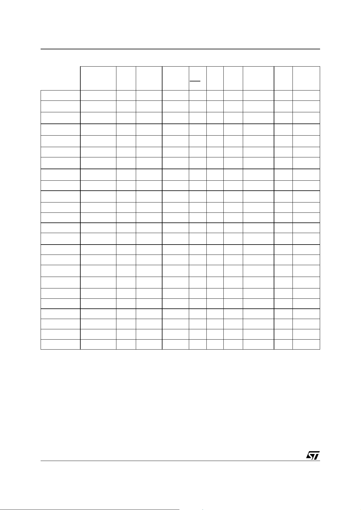
Table 1. Supervisor Options
Active
3V or 5V
Supervisor
Battery
Switch
over
Watchdog
Input
Watchdog
output
Active
Low
(1)
ST
R
STM690T/S/R 3V !! ! !
STM690A
STM692A
STM703
STM704
(3)
(3)
(4)
(4)
5V !! ! !
5V !! ! !
5V !!!!
5V !!!!
STM704T/S/R 3V !!!!
STM705
STM706
(5)
(5)
5V !!! !!
5V !!! !!
STM706T/S/R 3V !!! !!
STM706P
(6)
3V !! !!!
STM707 5V !! ! !
STM708 5V !! ! !
STM708T/S/R 3V !! ! !
STM795T/S/R 3V !
(2)
!
STM802L/M 5V !! ! !
STM802T/S/R 3V !! ! !
STM804T/S/R
STM805T/S/T
(7)
(7)
3V !!
3V !!
STM805L 5V !! ! !
STM806T/S/R 3V !!!!
STM813L 5V !! !!!
STM817L/M 5V !! ! ! !
STM818L/M 5V !! ! !!
STM819L/M 5V !!!!!
Note: 1. Push-Pull Output (unless otherwise specified).
2. Open drain output.
3. STM690A has a typical Reset Threshold of 4.65V and STM692A has a typical Reset Threshold of 4.40V.
4. STM703 has a typical Reset Threshold of 4.65V an d ST M704 has a typical Reset Threshold of 4.40 V.
5. STM705 has a typical Reset Threshold of 4.63V an d ST M706 has a typical Reset Threshold of 4.38 V.
6. The STM706P is identical to the STM706R, except for i ts Re set output which is active High.
7. STM804T/S/R and STM805T/S/R have different minimum and maximum Reset Thresholds with V
datasheet).
High
RST
!
!
(1)
(2)
(2)
Manual
Reset
Input
Power-fail
Comparator
!
!
falling and VCC rising (see
CC
ChipEnable
Gating
!
Battery
Freshness
Seal
4/22
Page 5
AN1957 - APPLICATION NOTE
POWER-ON RESET AND LOW VOLTAGE DET ECT
After system start-up, a certain period of time is required for the power supply voltage to stabilize. For this
reason, ST Supervisor devices generate a Reset pulse after power-up (the minimum pulse width is
t
= 140ms, see Table 2.). Over the t
rec
the registers are set to their default values. This function is called Power-On Reset (POR).
Some designers attempt to use RC circuits, instead of a Reset implementation, because it is cheaper. But
it is also unsafe and u nreliable. RC circu its are not suitable fo r use as professional devi ces in industr ial
environments (see REFERENCES section, AN1772).
Another major function is Low Voltage Detect (LVD), which detects power supply brownouts and glitches.
Whenever V
after VCC increases above the V
falls below the Reset thres hold (V
CC
rst
is guaranteed. Also, if the triggering event is a narrow glitch, an RC circuit will only generate a poor Reset,
which may lead to malfunct ioning of the mi croprocess or (failing t o load registers correctly, ex ecuting invalid instructions, processing incorrect data, etc.).
Some Supervi sor devi ces in clude a Manua l Reset i nput (M
device, to generate a Reset. T ypically, a low-c ost push-button s witch is conne cted to the Manual Res et
input, which allows the user to restart the pr ocessor witho ut turning off the power. No add itional co mponents are needed becaus e Sup er viso r de vi ce s al ready inc lu de a deb oun ce circ uit that fil ter s the nois e of
contact closure. This fun ction c an be us ed to de bug , to pe rf orm the final test of a process or, or to r est art
a processor that is locked. The Reset button is also useful in systems where the processor is never turned
off, even when the system is in Off mode. Some processor s inclu de an interna l Reset that operates cor rectly under stable power supply conditions, but usually has difficulties in handling voltage drops and transients as well as looser tolerances for V
period, during which reset is asserted, the clock is stabilized and
rec
), the Reset output is ass erted and remains so t
RST
rec
threshold. In the case of an RC circuit, no minimum Reset pulse width
R) that can be used by the user, or the external
. The use of an external Reset is therefore recommended.
rst
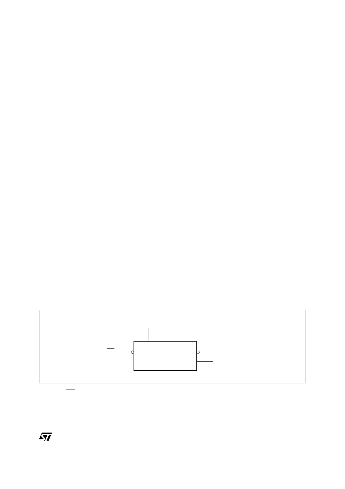
Block Diagram Showing the Supervisor Reset Feature
Figure 1 . illustrates the Power-On Reset, Low Vol tage Detect and Manu al Reset features. The Reset is
asserted if one of the following events occurs:
■ system start-up;
■ Brownout, voltage drop, significant transient or glitch, negative voltage spike etc. on the power supply
line;
■ Manual Reset.
Figure 1. Supervisor Reset Features
V
CC
RESET
Power-On Reset
Low V oltage Detect
RST
ai10104
Note: V
MR RST
is the supply voltage, MR i s the Manu al Reset input . RST and RST are Reset outputs. Supervi sor dev ices can have an ac tive-Lo w
CC
output (R
ST), an active-High output (RST) or both.
5/22
Page 6
AN1957 - APPLICATION NOTE
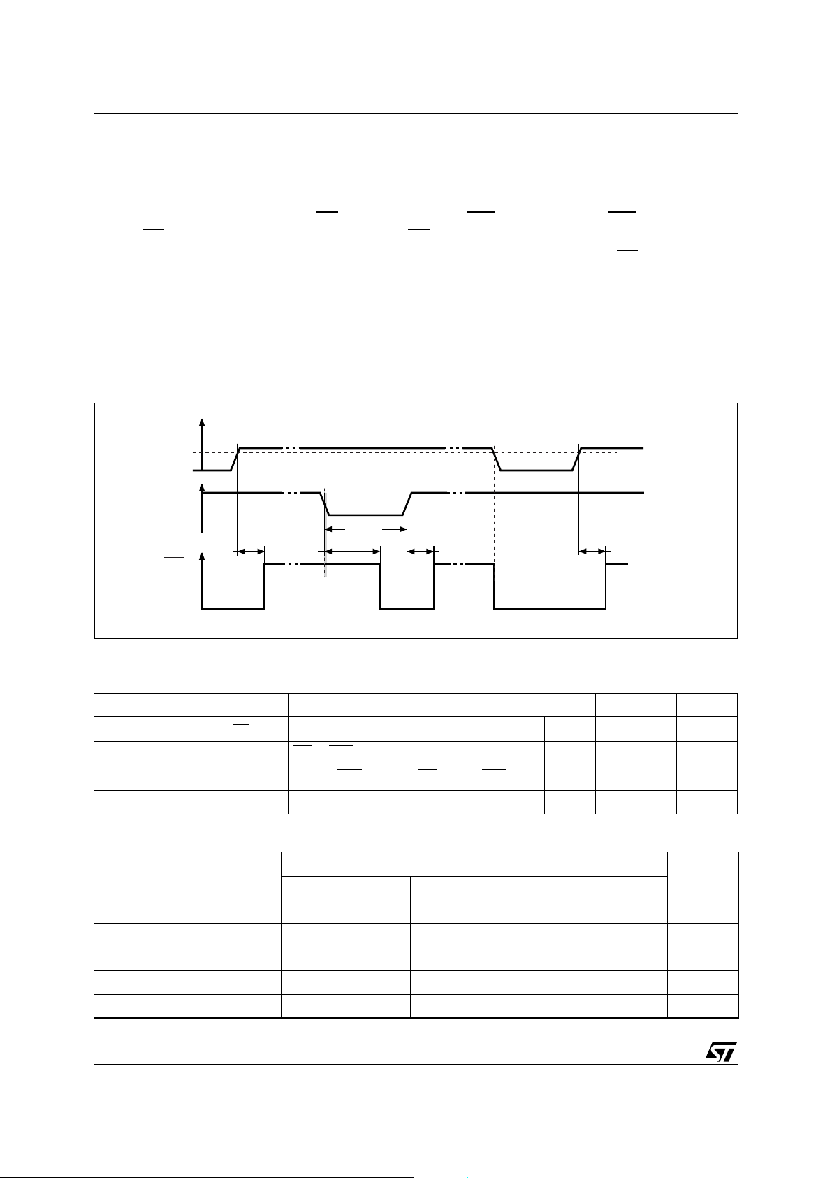
Reset Waveforms for the Microprocessor Supervisor Devices
When the input vol tage l evel re aches th e Re set th reshold (V
holds the Reset output signal (RST
) Low for a minimum time of t
2.).
Switching the Manual Reset signal (M
long as MR
is kept Low, and returns High t
R) to Low, causes the RST signal to go Low. RST remains Low as
after MR has been released.
rec
All Microprocesso r Supervisor device s have glitch immunit y. That is, the minimum MR
quired to Reset the output is fixed. All shorter pulses are ignored.
The Supervisor also r eacts to vol tage drops, brow nouts a nd signific ant glitc hes. If the inpu t voltage fa lls
below V
, the Reset output is asserted.
RST
Note that some Supervisor devices have a Reset output that is active High (RST). They therefore have a
waveform that is the inversion of the one that is shown in Figure 2.
Figure 2. Power-On Reset and Low Voltage Detect Waveforms
) after system power-up, the Super visor
RST
before driving it High again (see Figure
rec
pulse width re-
CC
Power-up
t
rec
Manual Reset
t
MLRL
Manual Reset
Glitch Immunity
t
MLMH
t
rec
Voltage drop
t
rec
Note: V
V
V
RST
MR
RST
is the Reset threshold, see Table 3. for values.
RST
Table 2. Reset Timings for the STM703/704 Supervisor
Symbol Alt Parameter Value Unit
t
MLMH
t
MLRL
t
rec
t
MR
t
MRD
MR Pulse Width Min. 150 ns
MR to RST Output Delay Max. 250 ns
V
to RST High and MR High to RS T High
RST
Min. 140 ms
Manual Reset Glitch Immunity Typ. 100 ns
AI10105
Table 3. Reset Thresholds (V
Supervisor
RST
)
Reset threshold (V
RST
)
Min. Typ. Max.
STM706P/70xR 2.55 2.63 2.70 V
STM70xS 2.85 2.93 3.00 V
STM70xT 3.00 3.08 3.15 V
STM692A/704/706/708, 8xxM 4.25 4.40 4.50 V
STM690A/703/705/707, 8xxL 4.50 4.65 4.75 V
6/22
Unit
Page 7

AN1957 - APPLICATION NOTE
Hardware Hookup for the STM703/704 Supervisor
In the example of Figure 3., the Reset output is asserted in three cases:
■ during system power-up, until V
■ after a V
■ by pressing the Manual Reset push-button (the Reset button should be held for at least for t
drop (VCC falls below V
CC
The Manual Reset input is not necessarily connected to a physical push button switch, it can also be connected to a peripheral, provided that a minimum MR
If the Res et cir cuit i s plac ed in a noi sy envi ronme nt, or if MR
to use an external 0.1µF capacitor, as shown in Figure 3.
The MR
input includes an internal pull-up resistor. So in applications where the MR input is not used, the
pin can be left unco nnected. The MR
drain output.
It is always appropria te to conne ct a deco upling c apacitor in parall el with the power su pply. Th e recommended value is 1µF.
Figure 3. Hardware Hookup for the STM703/704 Supervisor
is stabilized (VCC is greater than V
CC
)
RST
) for a duration of t
RST
rec
MLMH
pulse width of 150ns is ensured.
is driven from long cables, it is recommended
input can be driven with a T TL ou tpu t, a CMOS output, or an open
).
Microprocessor
V
GND
RST
CC
V
CC
C
1
1µF
STM703/704
1
OUT
V
2
CC
V
3
SS
PFI PF0
45
SO8/TSSOP8
V
BAT
RST
MR
8V
7
6
Reset
Button
C
2
0.1µF
AI10106
7/22
Page 8

AN1957 - APPLICATION NOTE
–
----
–
POWER-FAIL COMPARATOR
Inadvertent or unexpected power loss can cause a number of malfunctions in a system (data loss, uncontrolled program status, indeterminate processor state, etc.).
For a reliable design, sys tems should rece ive early power fail ure warning, to leave enough time for the
microprocessor to start a safeguard routine, for backing up crucial data, registers, etc.
Power-fail comparato rs are used to monitor unregulated powe r supplies. The ir reaction to power los s is
very fast, and can provide enough time to execute all the necessary safeguard processes that precede an
expected power failure (see REFERENCES section, AN1336).
Block Diagram of a Power-Fail Comparator
The power-fail comparator works like an ordinary comparator with hysteresis (see Figure 4.). The PowerFail Input (PFI) is compared to an internal reference voltage, the power-fail threshold, V
on PFI is less than V
, the Power-Fail Output (PFO) is assert ed.
PFI
Figure 4. Block Diagram of a Power-Fail Comparator
PFI
PFO
. If the voltage
PFI
V
PFI
ai10107
Hardware Hookup for the STM692A Supervisor
The Power-fail compa rator can be used i n many different ways . It is most comm only used as an Early
Power-Fail Warning (see Figure 5.) to monitor an unregulated supply voltage.
Two external resistors R
and R2 form a voltage divider to set the voltage level (V
1
) below which PFO
TRIP
is asserted (see the waveforms shown in Figure 6.).
Usually, a value is selected for R
V
R
×=
2
TRIPVPFI
--------------------------
V
PFI
R
1
, Where V
, then R1 is derived using the following formula:
2
= 1.25V.
PFI
The sum of the resista nces sh ould be ab out 1MΩ t o minimize power co nsumption , and the to lerance of
the resistor should not exceed 1%, to ensure that there are not large variations in the sensed voltage.
Example calculation.
We have: V
Let us put: R
R
is calculated as follows:
1
Thus R
= 820kΩ.
1
= 11.5V and V
TRIP
= 100kΩ
2
R
PFI
1
= 1.25V.
V
R
TRIPVPFI
----------------------------- -× 100 10
2
V
PFI
11.5 1.25–
3
--------------------------×⋅ 820kΩ== =
1.25
8/22
Page 9

AN1957 - APPLICATION NOTE
Table 4. Recommended Resistances for some V
V
(V) R1 (kΩ)R
TRIP
TRIP
Voltages
8.5 750 130
10.0 910 130
11.5 820 100
12.5 820 91
15.0 1100 100
Figure 5. Hardware Hookup for the STM692A Supervisor
~220V
~120V
Power
Supply
V
UNREG
R
V
PFI
Regulator
1
R
2
V
CC
STM692A
1
OUT
V
2
CC
V
3
SS
PFI PF0
45
SO8/TSSOP8
V
BAT
RST
WDI
(kΩ)
2
Microprocessor
V
C
1µF
8V
7
6
CC
NMI
GND
ai10108
9/22
Page 10

AN1957 - APPLICATION NOTE
Example of Power-Fail Waveforms
Figure 6 . shows the cas e of a voltage drop . The unregulated powe r supply voltage (V
decrease. As it falls below V
, at t0 in Figure 6., PFO is asserted, invoking a non-maskable interrupt in
TRIP
the microprocessor, and causing the execution of the safeguard routine. The mic roprocessor continue s
operating until Reset is asserted. From t
, the power supply volt age (VCC) starts to fall. At t2 Reset is as-
1
serted and Write Protect occurs. This means that the safeguard routine cannot last more than t
Figure 6. Voltage Drop
UNREG
) begins to
− t0.
2
V
UNREG, VCC
V
V
V
Note: At t0 the voltage drop is detected; at t1 VCC begins to fall; at t2 Reset is asserted and/or Write Protect occurs.
TRIP
RST
PFO
V
UNREG
V
CC
Voltage Drop
t
0t1t2
+12V
+11.5V
+5V
+4.4V
t
t
Table 5. Power-Fail Values for all Microprocessor Supervisors (except
for the devices mentioned in Table 6.)
Symbol Parameter Value Unit
V
PFI
Power-fail threshold Typ. 1.25 V
ai10109
Table 6. Power-Fail Values for 3V Microprocessor Supervisors
with Battery Switchover (STM690/704/802/804/805/806)
Symbol Parameter Value Unit
10/22
V
PFI
Power-fail threshold Typ. 1.237 V
Page 11

AN1957 - APPLICATION NOTE
WATCHDOG TIMER
The role of a Watchdog timer is to prevent system failures that are ca used by certain typ es of hardwar e
errors (non-responding peripherals, bus contention etc.) or software errors (bad code jump, code stuck in
loop etc.).
The watchdog timer has an input, WDI, and an output, WDO
timer periodically wi thin the specifi ed time-out pe riod, t
correctly, it periodically toggles the Watchdog Input, WDI (see Figure 8.). If the system fails, the watchdog
timer is not reset, a nd a system alert is generated: the W atchdog output, W DO
asserted (see Figure 8.).
Some microprocessors have an integrated watchdog timer, with a time-out period that is software-adjustable. The great disadvantage of this solution, though, is that the integrated watchdog timer uses the same
power supply, and clock signal, as the microprocessor. So, a system malfunction may also lead to a failure
of the watchdog timer.
Figure 7. Logic Diagram of a Watchdog Timer
(see Figure 7.). The input is use d to clea r the
(see Table 7.). While the system i s operating
WD
, or the Reset output, is
WDI WDO
Note: 1. WDI is the Watchdog Input, WDO is the Watchdog Output.
Watchdog
timer
Figure 8. Watchdog Timer Input and Output Waveforms
Correct operation
of the system
WDI
WDO
Note: 1. WDI signal frequencies greater then 50MHz (20ns period) will be filtered.
2. t
is the Watchdog time-out period. See Table 7. for value.
WD
System
failure
t
WD
System
restart
Correct operation
of the system
Table 7. Watchdog Timer Time-out Value for the STM705 Supervisor
Symbol Description Value Unit
t
WD
Note: This tWD value is valid for all Microprocessor Supervisors.
Watchdog time-out period Typ. 1.6 s
ai10110
t
t
ai10111
11/22
Page 12

AN1957 - APPLICATION NOTE
Hardware Hookup for the STM705 Super viso r
WDI is usually connected to the output pin of the mi cr op ro ce ssor as sh own in Fi gure 5 . and WDO
to the microprocessor Non-Maskable Interrupt (N
MI) or Reset input.
The code should take care of clearing the watchdog timer within the time-out period by toggling the microprocessor’s I/O pin.
Figure 9. Hardware Hookup for the STM705 Supervisor
is tied
STM705
1
MR
2
V
V
3
PFI PF0
45
WDO
8
RST
CC
SS
SO8
RST
7
WDI
6
), WDO goes Low even if the w atchdo g time r
ai10112
In any case, if V
Microprocessor
V
CC
I/O
NMI
drops below the Res et threshol d (V
CC
C
1µF
has not timed out. The ti mer remains cleared and do es not count fo r as long as Re set is asserted . The
counter automatically restarts after t
expires.
rec
In 5V supply devices, the watchdog function may be disabled by floating WDI or tri-stating the driver that
is connected to WDI.
12/22
Page 13

AN1957 - APPLICATION NOTE
BATTERY SWITCHOVER
A common task of battery switchover devices is to provide an uninterrupted power supply to external devices in the event of voltage drops and brownouts.
Battery switchover devices can also be useful in portable devices. When the external power supply (such
as the AC power supply adapte r) is disconn ected, the bat tery switcho ver devic e switches to the internal
supply (such as a battery).
The use of a battery switchover has the following advantages:
■ providing continuous and reliable service, even if the external supply fails
■ extending the battery lifetime
■ debouncing the power spikes occurring while connecting and disconnecting the AC adapter.
Battery switchover devices can be used as a main power supply backup for MCUs, memories and other
peripherals, and to prevent system failures (see Figure 10.).
Diode-OR connections are often use d as an equiv alent soluti on. However th e diode vol tage drop rep resents a large percentage of the battery voltage, and power supply spikes are not filtered. With an ST Supervisor, the device is supplied from the main powe r supp ly as long as the vo ltage is high en ough, ev en
if the battery voltage is greater than the power supply voltage, which sa ves the battery and extends its
lifetime.
Instead of a backup battery it is also possible to use a backup capacitor. Recommended capacitor values
start from 0.1F.
The battery switch over device monitor s the power supp ly voltage , V
ence voltage, V
voltage, V
BAT
, as shown in Figure 11. If VCC drops too low, the V
SO
. The comparator includes hysteresis for noise immunity purposes.
, which is compared t o the refer-
CC
output is switched to the battery
OUT
Figure 10. Block Diagram of a Battery switchover Device
V
CC
V
BAT
V
SO
V
OUT
ai10113
13/22
Page 14

AN1957 - APPLICATION NOTE
Switchover Waveforms for the STM806R Supervisor
The Battery Backup Switchover Voltage (V
ver Threshold, V
V
, VSO is equal to V
BAT
Whenever V
CC
(see Figure 11.). If VSW is lower than V
SW
.
BAT
falls below VSO, the V
OUT
Figure 11. Battery Switchover Waveforms for the STM806R Supervisor
V
V
CC
,
BAT
) depends on the Battery Voltage (V
SO
, VSO is equal to VSW. If VSW is greater than
BAT
output is connected to the battery, V
) and on the Switcho-
BAT
(see Figure 11.).
BAT
V
V
BAT
then V
V
BAT
V
SW
V
SO
Voltage
V
OUT
V
SW
Note: The red line represents the switchover voltage (VSO). The blue line represents the battery switchover circuit output voltage (V
which is switched to V
Drop
, or to V
CC
,
>
SW
= V
SO
SW
depending on the voltage magnitude.
BAT
V
BAT
then V
<
V
SW
= V
SO
Voltage
Drop
,
BAT
V
CC
V
SO
V
OUT
V
V
CC
BAT
ai10114
OUT
),
14/22
Page 15

AN1957 - APPLICATION NOTE
STM806R has a voltage hysteresis of 40mV, which gives it good noise immunity. The hysteresis depends
on V
■ If V
■ If V
Figure 12. Switchover Waveforms with Hysteresis Details
and VSW as illustrated in Figure 12.:
BAT
> VSW and VCC falls, the battery switchover detects the switchover threshold VSW and switches
BAT
V
to the backup battery supply. When VCC rises, the voltage level VSW + 40mV is detected and
OUT
V
is switched back to the main power supply (VCC).
OUT
< VSW and VCC falls, the battery switchover detects the voltage level V
BAT
switches V
detected and V
V
CC, VBAT
V
SW
V
OUT
to the backup battery supply. When VCC rises, the voltage level V
OUT
is switched back to the main power supply (VCC).
OUT
V
> V
BAT
SO
SW
= V
then V
V
BAT
V
SO
Voltage
Drop
− 75mV and
BAT
− 35mV is
BAT
,
SW
V
BAT
then V
< V
SO
SW
= V
,
BAT
Voltage
Drop
V
CC
V
SO
V
V
SW
V
CC
V
CC
V
BAT
V
SW
V
CC
V
OUT
V
SW
+ 40mV
V
BAT
V
CC
V
SW
V
BAT
− 75mV
OUT
V
CC
V
BAT
Table 8. Switchover Values for the STM806R Supervisor
Symbol Description Condition Typical Value Unit
V
SW
V
hys
V
SO
Threshold 2.4 V
Hysteresis 40 mV
V
Battery Backup Switch ov er Voltage
< V
BAT
SW
V
> V
BAT
SW
VSO = V
VSO = V
BAT
SW
V
OUT
V
− 35mV
BAT
ai10115
V
V
15/22
Page 16

AN1957 - APPLICATION NOTE
Hardware Hookup for the STM806R Supervisor
Figure 13. shows one pa rticular hardw are hookup, usin g the STM806R Supe rvisor to s witch the power
supply source, with good efficiency and without introducing any switching noise.
In this case, the battery switchover backups the main power supply of MCU, memories and other periph-
erals. If sufficient p ower is avail able fro m the bac kup sup ply, t he sy stem can contin ue w orking normall y.
However it is also possible to run a safeguard routine, and to force the system to the low-power mode, so
that the backup power supply can last longer, until the main power supply is restored.
Figure 13. Hardware Hookup for the STM806R Supervisor
V
CC
SRAM
V
CC
GND
C
1µF
STM806R
1
OUT
2
V
CC
3
V
SS
45
PFI PF0
SO8/TSSOP8
V
BAT
RST
MR
8V
7
6
3V Battery
AI10263
Hardware Hookup for the STM795 Supervisor
The V
possible to use the Vccsw
output is able to s witch 75mA (m aximum). If the peripheral s have greate r current needs , it is
OUT
output of the STM795 device, and to drive the gate of the external PMOS tran-
sistor (as shown in Figure 14.).
When V
switches to the battery, the Vccsw goes High. When V
OUT
switches back to VCC, Vccsw goes
OUT
Low again, and the transistor provides current directly from the power supply.
Figure 14. Hardware Hookup for the STM795 Supervisor
V
CC
Microprocessor
V
CC
GND
SRAM
V
CC
GND
C
1µF
STM795R
1
OUT
2
V
CC
3
V
CCSW
45
V
SS
SO8/TSSOP8
E
V
BAT
RST
CON
E
8V
7
6
3V Battery
16/22
AI10264
Page 17

AN1957 - APPLICATION NOTE
CHIP ENABLE GATING
Internal gating of the chip ena ble sign al preven ts erroneo us data fro m corrupti ng the exter nal SRA M, in
the event of an under-voltage condition. The chip enable signal, which normally goes directly from
the microcontr ol le r to the S RAM , i s rou t ed ins tea d th ro ugh the Sup er vis or dev ic e. The s ho rt p ropag ati on
delay enables the chip enable gating to be used with most microcontrollers.
During normal operati on ( when Re se t i s no t as s erted ), the Ch ip Enable signal is tr an sm itt ed thr ou gh the
Supervisor device unaltered. When Reset is asserted, the SRAM is placed in its low power mode and the
memory is inaccessible. In this way, the SRAM contents are protected from data corruption.
Chip enable gating uses a series transmission gate from E
ation (with Reset not asser ted), the E
time, the impedance of E
appears as a resistor, typically about 40Ω, in series with the load at E
transmission gate is enabled , and passes all E transition s. At that
to E
When Reset is asserted, the transmission path becomes disabled. In the disabled mode, E
impedance, the tran smis sion gate is tu rned off, a nd an act ive pull-up con nects E
up turns off again, when the transmission gate is enabled.
Figure 15. Chip Enable Gating Block Diagram
V
V
CC
RST
Comparator
t
rec
Generator
(see Figure 15.). During normal oper-
CON
becomes high
CON
to V
. This pull-
OUT
CON
RST
V
OUT
.
E
Note: Connect E to VSS if unused.
E
CON
Output
Control
E
CON
AI10265
17/22
Page 18

AN1957 - APPLICATION NOTE
Typical Waveforms for the STM818 Supervisor
After power-up, the E
the E
input signal on.
output stays High for a period of t
CON
While Reset is asserted, the chip-enable transmission gate is disabled, E
pull-up connects E
quence (when V
mediately becomes hi gh impedance. I f E
to V
CON
passes the Reset threshold), the chip-enable transmission gate is disabled, and E im-
CC
(disabled mode). If the voltage at E is High during a Power-down se -
OUT
is Low when Reset is asserted, the ch ip-enable transmission
gate will be disabled 15µs after Reset is asserted. This permits the current write cycle to complete during
power-down.
Any time a Reset is ge ner at ed, the c hi p- en abl e tran sm is si on gat e r ema in s d is abl ed , and E
impedance (regardless of any activity on E
the chip-enable transmi ssion gate depe nds on V
and the loading on E
. For the minimum propagation delay, minimize the capacitive load on E
CON
) for the Reset time-out period. The propagation delay through
, the source impedanc e of the drive c onnected to E,
CC
use a low-output impedance driver.
Figure 16. Typical Waveforms for the STM818 Supervisor
V
V
CC
RST
(see Figure 16.). After this it starts to pass
rec
is high impedance, and an active
remains high
CON
and
E
CON
V
BAT
RST
E
Note: The chip enable gating function is also implemented on the STM795 device. Nevertheless there are two differences, in comparison to
the STM818. Firstly the E
disabled only 10µs after Reset is asserted if the E
t
rec
signal is held High only for half of the t
CON
input is Low.
V
BAT
15µs
t
rec
AI10266
period, and secondly the chip-enable transmission gate is
REC
Table 9. Typical values for the STM818 Supervisor
Description Typical Value Unit
E
-to-E
Reset-to-E
-to-E
E
E
CON
Resistance
CON
High Delay (Power-down)
CON
Propagation Delay
CON
Short Circuit Current
40 Ω
15 µ s
2ns
0.75 mA
18/22
Page 19

AN1957 - APPLICATION NOTE
Hardware Hookup for the STM818 Supervisor
Figure 17. illustrates the hookup of the STM818 Supervisor circuit connected to a microprocessor and an
SRAM memory . All th e functi ons of the STM8 18 are u sed (bat tery sw itch over, w atchd og, ch ip enabl e gating, Power-On Reset, Low Voltage Detect).
The Chip Enable signal is de coded by the Ad dress De coder and i t goes to the E
circuit. The E
output is connected to the CS (Chip Select input) of the SRAM memory.
CON
Figure 17. Hardware Hookup for the STM818 Supervisor
V
Microprocessor
V
CC
A0-A15
I/O
RST
GND
Address
Decoder
CC
C
1µF
STM818
1
OUT
2
V
CC
3
V
SS
45
EE
SO8/TSSOP8
V
BAT
RST
WDI
CON
8V
7
6
input of the Superviso r
3V Battery
SRAM
A0-Axx
V
CC
CS
GND
AI10267
19/22
Page 20

AN1957 - APPLICATION NOTE
BATTERY FRESHNESS SEAL
The battery Freshness Seal is a feature that is available on the STM817/818/819. It disconnects the backup battery from the internal circuitry and V
Manufacturer) to ensure that the backup battery connected to V
is put to use.
To enable the Freshness Seal on the STM817 and STM819:
1. Connect a battery to V
BAT
2. Ground PFO
3. Bring VCC above the Reset threshold voltage, and hold it there until Reset is deasserted, following the
Reset timeout period
4. Bring V
Low again (see Figure 18.).
CC
For the STM818, use the same procedure, but ground E
Once the battery Fre shness Seal has e nabled (disconnec ting the backup batte ry from internal circuitry
and anything that is connected to V
OUT
Figure 18. Typical Waveforms for the STM817/818/819 Supervisors
V
V
CC
RST
until it is needed. This allows an OEM (Original Equipment
OUT
will still be fresh when the final product
BAT
instead of PFO.
CON
), it remains enabled until VCC is next brought above V
RST
.
t
rec
RST
AI10268
Note: 1. For the STM818, E
function is enabled.
2. For the STM817 and STM819, PFO
Freshness Seal function is enabled.
is held Low, externally. The E
CON
is held Low, externally. The PFO state is latched half way through the t
state is latched half way thr ough the t
CON
period, and the Freshness Seal
REC
period, and the
REC
CONCLUSION
ST Microprocessor Supervisors have a large range of features adapted to the user’s needs:
■ Centralised function for managing a system Reset.
■ Early warning of power failure, in time to initiate any safeguard routines.
■ Watchdog timer, monitoring for cessation of normal processor activity.
■ Battery switchover, either to allow continued operation, or to maintain minimum functionality. Also
useful for the regulation of noisy power supplies.
■ Battery Freshness Seal, for maintaining the battery life on the production line, for the end user.
ST Microprocessor Supervisors are the ideal choice for adding protection to applications that are used in
noisy environments and require power supply monitoring for proper operation.
20/22
Page 21
REFERENCES
■
AN1772
: How to Control Power-up/Reset and Monitor the Voltage in Microprocessor Systems using
ST Reset Circuits.
■
AN1336
: Power-Fail Comparator for NVRAM Supervisory Devices.
REVISION HISTORY
Table 10. Document Revision History
Date Version Revision Details
15-Mar-2005 1 First issue
AN1957 - APPLICATION NOTE
21/22
Page 22

AN1957 - APPLICATION NOTE
If
this d
MPG
you have any questions or suggestions concerning the matters raised in
ocument, please refer to the
request support web page:
http://www.st.com/askmemory
Information furnished is be lieved to be a ccur ate and reli able. Howe ver, STMicroele ctronic s assu mes no r esponsib ilit y for th e consequences
of use of such information nor for any infrin gement of patent s or other rights of third parties which ma y result from it s use. No license is granted
by implication or otherwi se under any patent or patent rights of STMicroelectronics. Specifications mentioned in this publication are subject
to change without not ice. This pub licat ion su persed es and repl aces all in format ion previou sly su pplie d. STMicroele c tronic s prod ucts ar e no t
authorized for use as critical compone nts in life support devices or systems without express written approval of STMicroelectronics.
The ST logo is a registered trademark of STMicroelectronics.
All other names are the property of their respective owners
© 2005 STMicroelectronics - All rights reserved
Australia - Belgium - Brazil - Canada - China - Czech Republic - Finland - France - Germany - Hong Kong - India - Israel - It aly - Japan -
Malaysia - Malta - Morocco - Singapore - Spain - Sweden - Switzerland - United Kingdom - United States of America
STMicroelectronics group of companies
www.st.com
22/22
 Loading...