

Page 1
AN1948
Obsolete Product(s) - Obsolete Product(s)
®
- APPLICATION NOTE
DVD Combo Power Supply with VIPer53
A. Bailly - S. Luciano
Despite the s trong growth of t he DVD readers, the VCR ones are still present o n the marke t. A lot of
equipment now includes both types of media in the same case. This paper proposes a typical solution to
efficiently supply such applications and other equipment where logic, DC motor drive and LCD display
are to be implemented together in the 35W power range and suite any input voltage standard (85Vac to
265Vac).
Key features for this application are high efficiency, low st andby consumption and cost effective solutions
to fit the high volume consumer market needs.
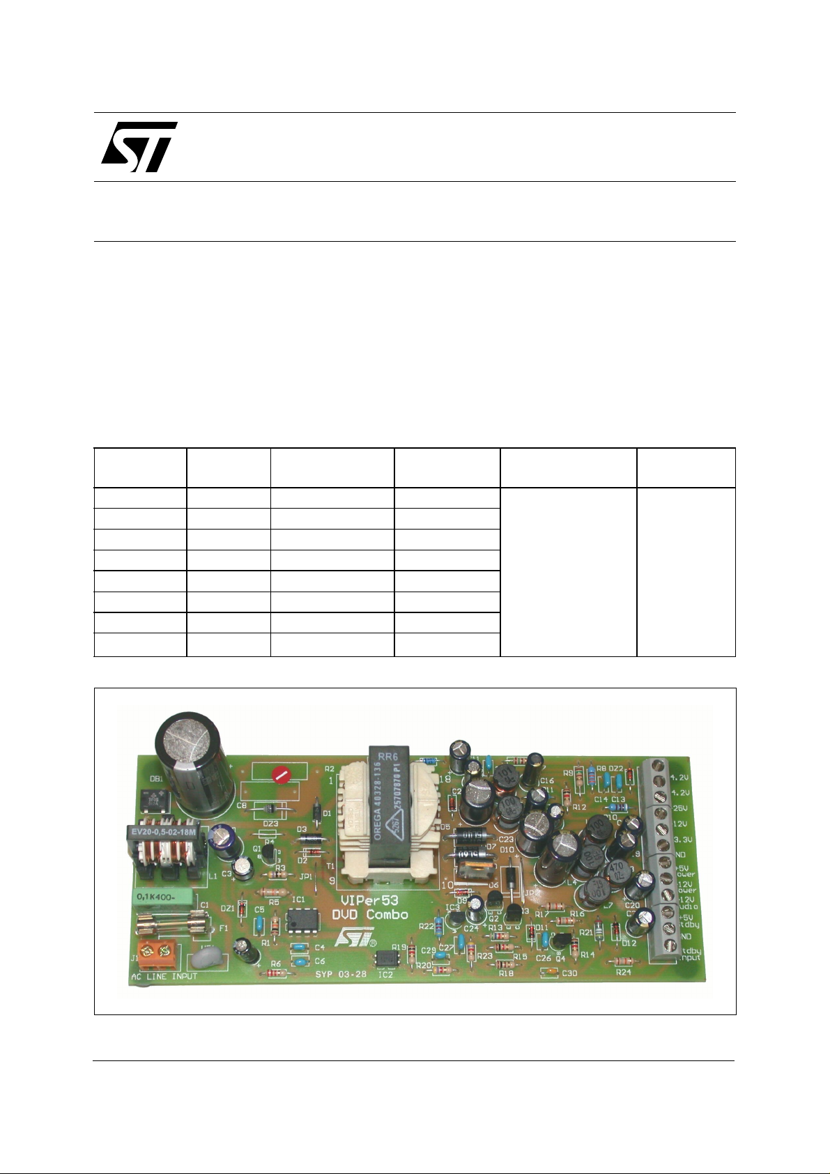
The specification can be summarized as shown in the following table:
Voltage
+/-5%
Output 1 3.3V 1.5A 4.95W
Output 2
Output 3
Output 4
Output 5
Output 6
Output 7
Output 8
5V Stand-by 100mA 500mW
5V Power 1.5A 7.5W
12V Power 1.5A 18W
12V Audio 200mA 2.4W
-12V Power 15mA 180mW
-25V 25mA 625mW
4.2V Display 50mA 210mW
Maximum Curr ent Outp ut Po wer MaximumPower Board S i ze
L x W x H
Normal Operation:
35W max output
power
Stand-by Operation:
750mW max input
power
With 40mA on the
5VStandby output
170x 70 x 40
(mm)
April 2004 1/17
Page 2
Obsolete Product(s) - Obsolete Product(s)
AN1948 - APPLICATION NOTE
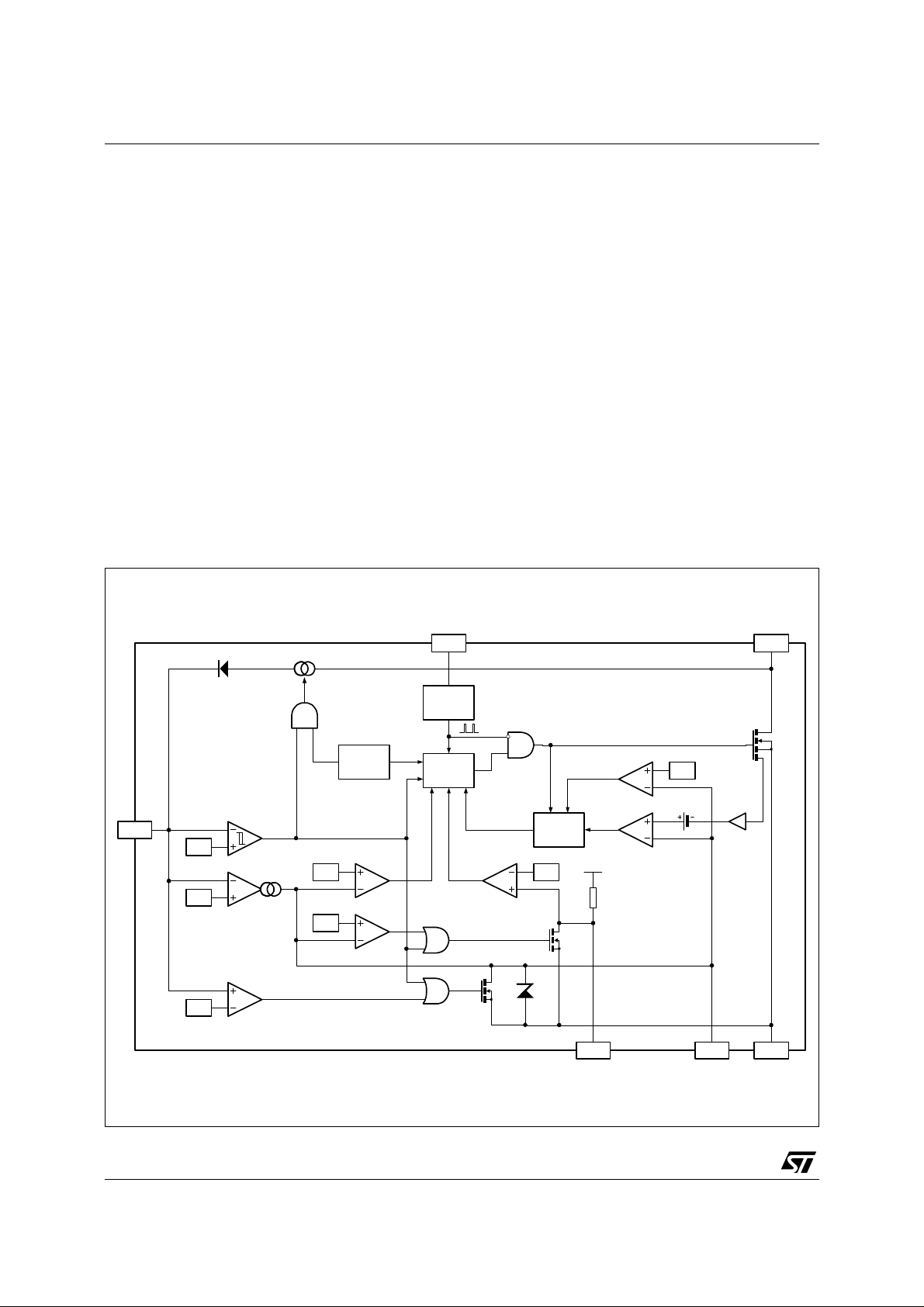
1. VIPer53 D ESCR IPTION
VIPer53, the first multichip device of the VIPer family has been chosen to fulfill the requirements. It
features very low Rdson of 1Ω allowing to deliver up to 35W in wide range in a standard DIP -8 pack age
without a heatsink, answering the need f or high er efficiency and reduced space thanks to a lower power
dissipation.
1.1 General features
The block diagram is given in figure 1. An adjustable oscillator drives a current controlled PWM at a fixed
switching frequency. The peak drain current is set for each cycle by the voltage present on the COMP
pin. The useful range of the COMP pi n extends from 0.5V to 4.5V, with a corres ponding drain current
range from 0A to 2A.
This COMP pin can be either used as an in put wh en working i n sec ondary f eedback conf iguration, or as
an output when the internal error amplifier co nnected on the VDD pin operates in primary feedba ck to
regulate the VDD voltage to 15V.
The VDD undervoltage comparator drives a high vol tage startup current source, which is switched off
during the norm al o pera tion of the devic e. Th is fe ature toge ther wi th th e burs t mod e c apabilit y allo ws t o
reach very low level of input power in standby mode, when the converter is lightly loaded.
Figure 1: VIPer53 block diagram
OSC DRAIN
ON/OFF
OSCILLATOR
PWM
LATCH
S
R1
FF
R2
R3 R4 R5
Q
4.5V
VDD
8.4/
11.5V
15V
18V
UVLO
COMPARATOR
ERROR
AMPLIFIER
OVERVOLTAGE
COMPARATOR
0.5V
4.35V
OVERTEMP.
DETECTOR
STANDBY
COMPARATOR
OVERLOAD
COMPARATOR
BLANKING TIME
SELECTION
150/400ns
BLANKING
4V
PWM
COMPARATOR
8V
125k
TOVL COMP SOURCE
1V
0.5V
H
COMP
CURRENT
AMPLIFIER
2/17
Page 3

Obsolete Product(s) - Obsolete Product(s)
AN1948 - APPLICATION NOTE
1.2 Overload protection
A threshold of 4.35V typical has been i mplem ente d on t he CO MP pin . This ov erload thresho ld is 150 mV
below the clamping voltage of 4.5V which corresponds to the current limitation of the device. In case of a
COMP voltage exceeding the overload threshold, the pull up resistor on the TOVL pin is released and the
external capacitor connected on this pin begins to charge. When a valu e of 4V typical is reac hed, the
device stops switching and remains in this state until the VDD voltage reaches VDDoff, or resumes
normal operation if the COMP voltage returns to a value below the overload threshol d. The drain current
that the device is a ble to deliver wit hout triggering the overl oad threshold is c alled "current capabilit y",
specified as IDmax in the datasheet. This value must be used to correc tly size the converter versus its
maximum output power.
When an overload occurs on secondary side of the converter, the output power is first limited by the
current limitation of the device. If this overload lasts for more than a time constant defined by a c apacitor
connected on the TOVL pi n, the dev ice is reset , a nd a new res tarting s equence is initiated by turning on
the startup current source. The capacitors on the VDD pin and on the TOVL pin will be defined together
in order to insure a correct startup and a low restart duty cycle in overload or short circuit operation. Here
are the typical corresponding formulas:
–
C
C
C
OVL
VDD
VDD
12.5 10
⋅⋅ ⋅>
810
I
DD1
---------------------------
>
V
DDhyst
Where tss and DRST are respect ively the time needed for the output voltages to pass from 0V to their
nominal values at startup, and the restart duty cycle in overload or short circuit condition. A ty pical value
of 10% is generally set for this last parameter, as it insures that the output diodes and the transformer
don’t overheat. The other parameters can be found in the datasheet of the device.
As the VDD capacitor has to respect two conditions, the m aximum value will be retained to define its
value.
1.3 Stand-by operation
On the opposite load configuration, the converter is lightly loaded and the COMP voltage decreases until
it reaches the shutdown threshold typically at 0.5V. At this point, the switching is disabled and no more
energy is passed on secondary side. So, t he output voltage decreases and t he regulation loop rises
again above the shutdown threshold, thus resuming the norm al switching operation. A burst mode with
pulse skipping takes plac e, as lo ng as the output power i s below the one correspond ing to the minimum
turn on of the device. As the COMP voltage works around 0.5V, the peak drain current is very low (it is
actually defined by the minimum turn on time of the device, and by the primary inductance of the
transformer) and no audible noise is generated.
In addition, the minimum turn on time depends on the COMP voltage. Below 1V (VCOMPbl), the blanking
time increases to 400ns, whereas it is 150ns for higher voltages. The minimum turn on times resulting
from these values are respectively 600ns and 350ns, when taking into account the internal propagation
time. This feature brings the following benefits:
- this brutal change induces an hyste resis between normal operation and burst mode which i s reached
sooner when the output power is decreased.
- a short value in normal operation insures a good drain current control in case of short circuit on
secondary side.
- long value in standby operation reinforces the burst mode by skipping more switching cycles, thus
decreasing switching losses.
More details regarding the standby operation can be found in the datasheet.
6
tss⋅⋅>
–
4
1
-----------------
–
D
tss⋅
1
RST
C
⋅
OVLIDDch2
------------------------------------------- -
V
DDhyst
3/17
Page 4
Obsolete Product(s) - Obsolete Product(s)
AN1948 - APPLICATION NOTE
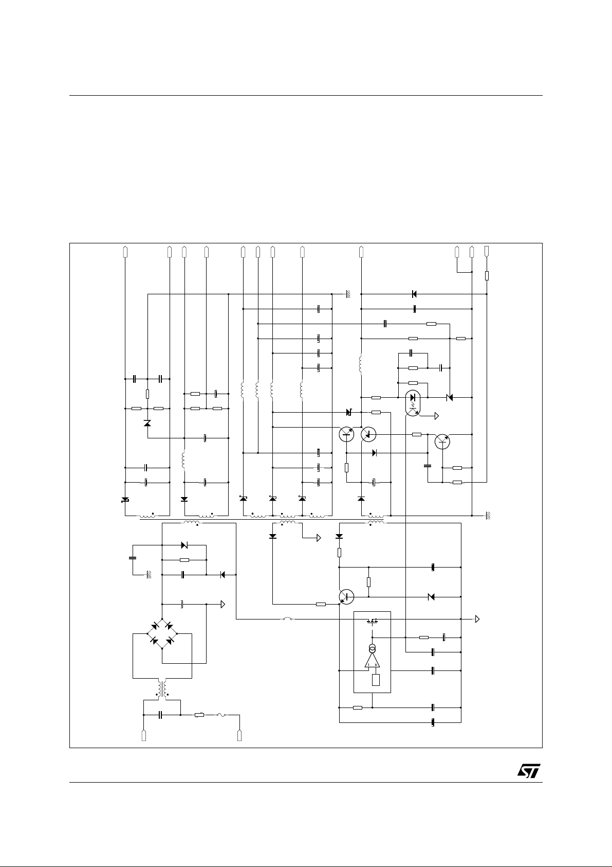
2.0 DVD COMBO POWER SUPPLY
2.1 Schematics
The power topology is an off line flyback work ing at a fixed switching frequency of 70kHz. The board
offers two operating modes. The normal one delivers 8 different output voltages and t he st andby one only
provides a 5V outpu t. This is achieved by a s mart standby management feature, based on a specific
transformer design which allows to dropout most of the output voltages, providing a low power
consumption in standby mode. The overall schematics is presented in figure 2.
Figure 2: schematics
J2-7
J2-8
J2-3
100nF
DZ2
J2-2
C14
100nF
R8
33k
R9
150
BZX79C5.1
C12
100nF
C11
10V
180µF
D5
J2-4
-25V / 25mA
+4.2V / 50mA
910
R11
910
R10
C16
39µF
L2
100µH
C15
39µF
BAV21
J2-1
-4.2V / 50mA
C13
R7
150
D4
BAT43
J2-9
-12V / 15mA
+12V audio / 0.2A
+12V power / 1. 5A
C17
35V
39µF
L3
47µHL410µH
1k
R12
35V
35V
D6
D8
STPS5L60
STPS8H100D
J2-5
+5V / 1.5A
+3.3V / 1.5A
C20
25V
120µF
25V
C19
120µF
C25
10V
180µF
C22
10V
180µF
L6
L5
10µH
10µH
25V
C18
820µF
C23
6.3V
1200µF
C21
6.3V
1200µF
D7
STPS5L40
J2-10
D12
+5V standby / 100mA
L7
10µH
100
R18
D10
1N5818
1K
R14
Q2
MPS2907A
D11
Q3
1N4148
PN2222A
R13
5.6k
35V
C24
39µF
D9
BAV21
1N4148
10V
C28
180µF
C30
6.8nF
1%
R21
4.99k
C29
10nF
R20
4.7k
1k
R19
IC2
1k
R15
C26
100nF
J2-6
J2-11
J2-12
GND
Standby
18k
R24
R23
4.7k
1%
R22
4.7k
C27
100nF
IC3
PC817
TL431LP
Q4
PN2222A
18k
R17
18k
R16
T1
OREGA
25707870P1
C9
1kV
2.2nF
DB1
DF08M
C1
J1-1
100nF
200
DZ3
BZT03C
R2
C8
C2
L1
0.5A
18mH
400V
D1
Not
Not
68µF
AC
1N4947GP
fitted
fitted
450V
33
F1
1A
VR1
250V
CT<0
IN
J1-2
D2
1N4148
JP1
D3
BYT01-400
0
R4
C10
250V
R5
Q1
18k
0.66W
2N5551
47
R3
DRAIN
VDD
IC1
VIPer53
R1
SOURCECOMPTOVL
15V
OSC
10k
4.7µF
10
DZ1
BZX79C
C7
R6
1µF
63V
2.2k
C6
10nF
C5
100nF
C4
2.2nF
C3
16V
47µF
4/17
Page 5

Obsolete Product(s) - Obsolete Product(s)
AN1948 - APPLICATION NOTE
2.1.1 Normal operation mode
In this mode, the Standby input is dri ven low, Q4 and Q2 are blocked and Q3 c onductis. All the ou tput
voltages are delivered to the loads and both 5V and 5VStandby outputs are provided.
The transformer turn ratio leads to a voltage of about 30V across C24. This voltage is blocked by Q2, and
the 5VStandby output is derived from the main 5V output through Q3. In the case where no load is
connected on the 5VStandby output, R14 allows to absorb the Q3 base current delivered by R13.
The same applies at primary side for the auxiliary supply of IC1. In normal operation, the VDD pin energy
is delivered by the stan dard auxiliary winding t hough D2. The c orresponding voltage is higher than the
one developed by the ze ner diode DZ1 on the base of Q1, and this transistor is blocked. In the m ean
time, the second auxiliary winding delivers five times more voltage than the one needed in standby mode
(see section 2.1.2), and values as high as 130V can be o bserved across C10. As a consequen ce, C10,
D3 and Q1 are high voltage type, and R5 may dissipate up to 1W.
2.1.2 Stand-by mode
All the output voltages are dropped down, except the 5VStandby one which is typically used to supply an
infrared receiver and its decoding circuit, and also to maintain the Standby input in the high state, which
makes Q4 and Q2 conducting, and disables Q3 thanks to D11.
As Q2 is conducting, the 5VStandby output is supplied through D9 and the corresponding winding o f the
main transformer. This winding therefore reduces its voltage by a ratio of about 5, because the regulation
loop still maintains the value of 5V on this output. Since all the outputs are coupled together on the same
transformer core, they are all divided by a ratio of about 5. This is sufficient to insure a reduced
consumption mode, as the loads are now supplied with a much lower voltage.
D11 is needed in this mode to efficiently turn off Q3. Otherwise, its base remains high as it is supplied by
R13 connected to a voltage of about 5V, and some reverse current flows from the 5V Standby output to
the main 5V one.
On primary side, the standard auxiliary winding doesn’t provide a sufficient voltage, and Q1 acts as a
serial regulator with the voltage delivered b y the second auxiliary winding, maintaining the VDD pin of
IC1 at higher level than the disabling threshold VDDoff. R14 on the 5VStandby output provides a
minimum consumption in this mode to insure a suitable voltage for Q1.
The transition between the normal mode and the standby mode has been slowed down by C26. Th is is
mandatory to avoid any under- or overvoltage on the out puts during this event. See also th e following
sect ion.
2.1.3 Regulation
The regulation sets the DC operating point from the 5VStandby output through R21 and R22. Note that it
would be difficult to implement a split regulation, as the other outputs operate with a different value when
in standby mode.
Some AC signals are also introdu ced int o t he r egu lat ion lo op t o ins ure stabilit y. The conventional pat h is
done through R18 connected to the 5VStandby output, but another AC component has been added
thanks to C30 and R23 conne cted on the 12V power output . This is needed to prevent any instability in
situations where the 5VStandby output is lightly loaded versus the 12V one. In order to transmit this
signal, a resistance R20 has also been added in series with the conventional capacitive feedback C27 at
the level of IC3.
The bandwidth of this regulation loop has been set at a few kHz in order to insure a good dynamic
response when submitted to load variations, or during the transitions between the normal mode and the
standby mode.
C29 on secondary side and C6 on primary side cancel any switching noise which may produce
subharmonic operation.
5/17
Page 6
Obsolete Product(s) - Obsolete Product(s)
AN1948 - APPLICATION NOTE
2.1.4 Drain voltage clamping
The board comes with a zener (DZ3) clamp type on the drain of the VIPer53 device. Provision is made to
also use an R-C type clamping network to replace this zener. The corresponding components R2 and C8
are to be populated according to the bill of material. See par. 2.3.1.
2.1.5 Short circuit protection
This paragraph only deals with the main outputs (i.e. all the 5V, 12V and 3.3V outputs). The following
section deals with the plasma ones.
When in normal mode, al l these out puts are protecte d agai ns t a perman ent short circuit. When the sho rt
circuit is applied on the 5V Standby, the short circuit current flows in to D10 which bypas ses Q3, thus
avoiding its destruction. The protection is done through the overload feature of the VIPer53 device, which
leads to hiccup mode when the COM P voltage remai ns high for a too long time. This time i s adjust ed by
the capacitor on the TOVL pin, and is needed at startup for authorizing a temporary overload during the
charge of the output capacitors.
In standby mode, only the 5VStandby output is protected thanks to D12 which forces the standby signal
in the low state, and the converter returns to the normal mode where Q2 is off. This is mandatory to avoid
the destruction of Q2 and D9 in this condition. The other out puts are not protected against a permanent
short circuit, because the converter can still regulate correctly the 5VStandby output even if one of the
others is short circuited. This is d ue to the high turn ratio existing between t he 5VStandby winding and
the other ones, and to the low consumption on this output . Nevertheless, the user will adopt one of the
following options:
- these outputs can withstand a short circuit for a few seconds. If this time is too long, the corresponding
rectifying diode may blow up, and the converter will enter into hiccup mode because of the short circuit
presented by the blown diode on secondary side of the transformer.
- addi tional diodes similar to D12 can be implemented on the other outputs to force the converter to the
normal mode, where it can withstand permanent short circuit on the main outputs.
2.1.6 Plasma display outputs
A whole set of outputs are dedicated to the driving of a plasma display in front of t he equipment: Negative
25V and 12V outputs, togethe r with a symmetrical +/-4.2V centered 5V high er than the -25V output
voltage.
Please note that these outputs are not protected against short circuits or overloads. For instance, the
short circuit of the 4.2V outputs to ground leads to the destruction of R7 or R9. Also, the rectifying diodes
chosen for these outputs don’t withstand a permanent short circuit.
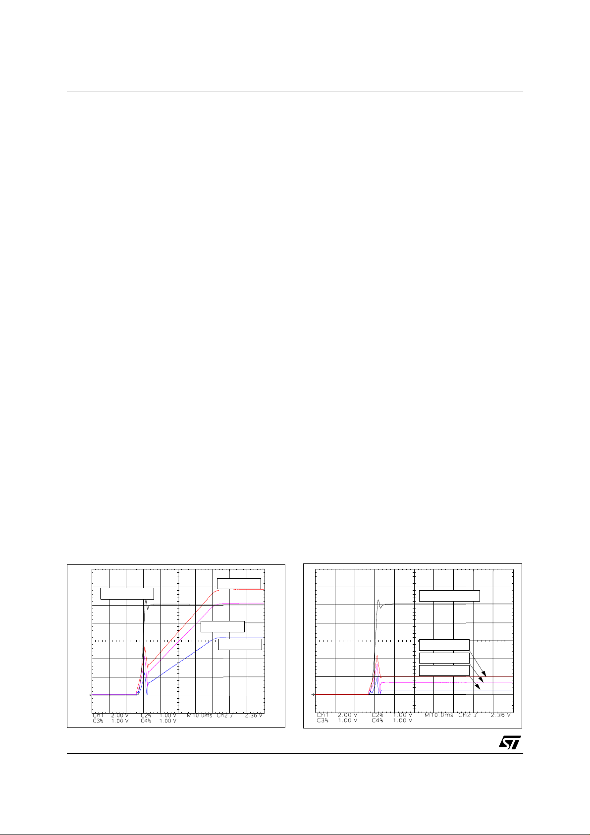
Figure 3: startup in normal mode Figure 4: startup in standby mode
Ch1 : 12V out
Ch2 : 5Vstby out
Ch3 : 5V out
Ch4 : 3.3V out
1
2
3
4
6/17
1
1
2
2
3
3
4
4
Ch2 : 5Vstby out
Ch1 : 12V out
Ch3 : 5V out
Ch4 : 3.3V out
Page 7

Obsolete Product(s) - Obsolete Product(s)
AN1948 - APPLICATION NOTE
2.2 Results
Unless otherwise specified, all the tests are made at 300VDC input voltage and full load.
2.2.1 Startup
When starting, C26 is discharged, an d t he conv erter operates in standby mode. S o, the 5V Standby voltage appears first, and the other out puts rise slowl y, just like a transition from a standby mo de to t he normal one. Of course, if the Standby signal is asserted hig h (active level), the converter remains in this
mode and only the 5VStandby output is delivered. This is illust rate d in figures 3 and 4.
The input voltage doesn’t impact on the dynamic behavior of the converter. The rising slope of the output
voltage at startup is mainly governed by the charge of C26 with the current defined by the base to emitter
voltage of Q4 together with R16 and R17.
2.2.2 Switch off
Figure 5 presents the output voltages at switch off of the conv erter. All the voltages drop down a t the
same time, because the converter doesn’t deliver any more energy. So, the slopes are individually driven
by the output capacitors and the output current.
Figure 5: switch off Figure 6: normal to stand-by mode transition
Ch1 : 12V out
Ch3 : 5V out
Ch2 : 5Vstby out
Ch4 : 3.3V out
1
2
3
4
1
2
3
4
Ch1 : 12V out
Ch3 : 5V out
Ch4 : 3.3V out
Figure 7: stand-by to normal mode transition Figure 8: load regulation
Ch1 : 12V out
Ch2 : 5Vstby out
Ch3 : 5V out
Ch4 : 3.3V out
5.5
5
4.5
4
V5V, V3.3V (V)
3.5
Ch2 : 5Vstby out
16
15
14
13
V12VPower (V)
12
V5VStandby
V5VPower
V3.3V
V12VPower
1
2
3
4
3
0 20 40 60 80 100 120
load (% full l oad)
11
7/17
Page 8

Obsolete Product(s) - Obsolete Product(s)
AN1948 - APPLICATION NOTE
2.2.3 Transitions between normal and stand-by modes
The standby input is quickly driven from low state to high state, and inversely. The corresponding
evolution of the output voltages are shown in figures 6 and 7. Note the very low disturbance on the
5VStandby output.
2.2.4 Load and cross regulation in norm al mo de
For these tests, the 12V audio output has always been let open. As it is connected almost in parallel with
the 12V power output (only a n L-C filter), it is assumed to follow the same vol tage variation than this
output, and its current is summed to the power one.
Also, load variation are only made on the main power outputs, that is to say the 5Vstandby, the 5V power,
the 3.3V and the 12V p ower ones. The -2 5Vand +/-4.2V s econdary outputs are either not loaded (load
regulation test) or fully loaded (cross regulation test).
The load regulation is c hecked by changing th e l oads on all the outputs simul taneously. This test is also
used for measuring the efficiency of the converter over a large range of output power. Figure 8 shows the
corresponding results for the four main outputs and figure9 the ones for the two secondary ones.
When not loaded, the converter operates correctly, except for the 12V and 3.3V outputs which do not
have any load. So, the corresponding voltages rise up respectively to 15.3V and 4.1V. If this is not
acceptable, the user has to foresee an adequate minimum load or a clamper.
Figure 9: cross regulation for secondary outputs Figure 10: 5VPowe r cross regulation
5
4.5
4
V4.2V (V)
3.5
3
0 20 40 60 80 100 120
Load (% full load )
27
26
25
24
V4.2V
23
V25V
V25V (V)
22
21
20
19
5.5
5
4.5
4
V5V, V3.3V (V)
3.5
3
0.001 0.01 0.1 1 10
I5VPower (A)
12
11.8
11.6
11.4
11.2
11
V12VPower (V)
V5VStandby
V5VPower
V3.3V
V12VPower
As the load on the secondary outputs is zero during this test, figure 9 shows the cross regulation between
the main outputs and the secondary ones. Note that the secondary output voltages don’t change
significantly versus their own load current, because these currents are low values, and these outputs are
already significantly loaded on the board itself. So, no load regulation is presented for the secondary
outputs.
The cross regulation between the main outputs has been measured. For this purpose, all the output are
loaded at intermediate level (half the maximum rated load), except one output which varies between zero
and maximum load. This test i s repeated for t he four ma in outputs and i s presented i n figures 1 0 to 13.
The result is also used for computing the relative efficiency for each main output.
8/17
Page 9

Obsolete Product(s) - Obsolete Product(s)
AN1948 - APPLICATION NOTE
Figure 11: 5VStandby cross regulat ion Figure 12: 3.3V cross regulation
5.5
5
4.5
4
V5V, V3.3V (V)
3.5
3
0 0.02 0.04 0.06 0.08 0.1 0.12
I5VStandby (A)
12
11.8
11.6
11.4
11.2
11
V12VPower (V)
V5VStandby
V5VPower
V3.3V
V12VPower
5.5
5
4.5
4
V5V, V3.3V (V)
3.5
3
0.001 0.01 0.1 1 10
I3.3V (A)
Figure 13: 12VPower cross regulation Figure 14: Global efficiency
5.5
5
4.5
4
V5V, V3.3V (V)
3.5
3
0.001 0.01 0.1 1 10
I12VPower (A)
15
14
V12VPower (V)
V5VStandby
V5VPower
V3.3V
V12VPower
13
12
11
10
85
80
75
70
65
60
Efficiency (%)
55
50
45
0 20 40 60 80 100 120
Load (% full load)
11.75
11.74
11.73
11.72
11.71
11.7
V12VPower (V)
V5VStandby
V5VPower
V3.3V
V12VPower
2.2.5 Efficiency in normal mode
The global efficiency is measured by varying all the outputs load simultaneously, except for the
secondary ones (-25V and +/-4.2V) which are n ot loaded in order to get the lowest values. Figure 14
presents the result.
Each cross regulation measurement is used for computing the relative efficiency Er on the corresponding
output by using the following formula:
P
outmaxPoutmin
--------------------------------------------------------=
E
R
P
The results are shown in the following table:
Er 77% 73% 80% 85%
–
–
inmaxPinmin
3.3V 5VStandby 5VPower 12VPower
9/17
Page 10

Obsolete Product(s) - Obsolete Product(s)
AN1948 - APPLICATION NOTE
The lower the output v oltage, the lower the relative efficiency bec ause of the fixed vo ltage drop in the
output rectifying diodes. The relative efficiency for the 5VStandby output is low when compared to the
other ones, because of two reasons:
1) it is derived from the 5VPower output, with a voltage drop in Q2 of about 100mV which leads to a loss
of 2% in efficiency.
2) when the output current on the 5VStandby increases, its output voltage remains fixed by the regulation
loop, and all the other outputs increase by 2%. So, the onboard dummy loads for the secondary
outputs (R7 to R12) increase by 5% (related to the 500mW of full load on the 5VStandby output), and
the relative efficiency is decreased by this figure.
Overall, the total efficiency is decrease by 7%, which corresponds to the difference between the
5VPower and the 5VSt andby outputs.
The efficiency has also been measured at full load and for an input voltage varying between 120Vdc and
400Vdc. The results are shown in figure 15.
Figure 15: efficiency Vs. input voltage Figure 16: load regulation and input power in
standby mode
85
80
75
70
Efficiency (V)
65
60
100 150 200 250 300 350 400 450
Vin (V)
5.2
5.15
5.1
V5V (V)
5.05
5
0 0.02 0.04 0.06 0.08 0.1 0.12
I5VStandby (A)
1600
1200
800
400
0
Pin (mW)
V5VStandby
Pin
2.2.6 Load regulation and input power in standby mode
As there is only one active output in standby mode, th ere is no cros s regulation m easurement . Instead,
the input power is measured to check its compliance versus specific energy saving standards like Energy
Star or Blue Angel. Both output voltage value and input power are shown in figure 16.
All the other outputs are not loaded. The user will pay attention to its real load, which may consume some
power in this condition: Even if the voltages are reduced by a ratio of five or more, they are still able to
deliver the rated current!
At 300Vdc input voltage, the converter always works in burst mode in standby condition. This mode is
characterized by the fact that the device skips some switching cycles, as shown in figure 17. The
magnification in figure 18 presents a conduction time of 700ns, which correspond s to the long blanking
time of the VIPer53 device, as the COMP voltage operates around the shutdown value (0.5V typical),
well below the blanking value threshold (1V typical). Also note the reduced reflected value versus the
normal full load switching cycle in figure19.
10/17
Page 11

Obsolete Product(s) - Obsolete Product(s)
AN1948 - APPLICATION NOTE
Figure 17: burst mode in standby condition Figure 18: Magnification of a switching cycle in
standby condition
Ch1 : Vds
Ch1 : Vds
1
1
2.2.7 Line regulation
The output voltage has been measured at full load for an input voltage varying between 120Vdc and
400Vdc for both power (figure 20) and secondary (figure 21) outputs.
4
Ch4 : Ids
Figure 19: normal full load switching cycle Figure 20: Line regulation for the main outputs
5.5
5
Ch1 : Vds
1
4
Ch4 : Ids
4.5
4
V5V, V3.3V (V)
3.5
3
100 150 200 250 300 350 400 450
Vin (V DC)
12
11.9
11.8
11.7
11.6
11.5
V12VPower (V)
V5VStandby
V5VPower
V3.3V
V12VPower
2.2.8 Dynamic load variation
Each main output h as been submitted to fast load variation between 10% and 100% of their rated full
load. All the others are loaded with a fixed current corresponding to half load . Results are presented in
figures 22 to 25.
11/17
Page 12

Obsolete Product(s) - Obsolete Product(s)
AN1948 - APPLICATION NOTE
Figure 21: line regulation for secondary outputs Figure 22: 5VPowe r dynamic load regulation
4.45
4.4
4.35
V5V, V3.3V (V)
4.3
4.25
100 150 200 250 300 350 400 450
Vin (V DC)
26
25.75
25.5
25.25
25
Ch2 : V5VPower
V25V
V4.2V
V12VPower (V)
Ch4 : I5VPower
4
Figure 23: 5VStandby dynamic load regulation Figure 24: 3.3V dynamic load regulation
Ch2 : V3.3V
Ch2 : V5VStandby
Ch4 : I3.3V
Ch4 : I5VStandby
4
4
2.2.9 Stability
An example of stability measurement is presented in figure 26 at full load. The phase margin is about 50°
with a gain margin of about 10dB.
12/17
Page 13

Obsolete Product(s) - Obsolete Product(s)
AN1948 - APPLICATION NOTE
Figure 25: 12V dynamic load regula tion Figure 26: gain and phase plot at full load
100
80
Ch2 : V12VPower
Ch4 : I12VPower
4
60
40
Gain (dB)
20
0
-20
1 10 100 1000 10000 100000
150
100
50
0
-50
-100
-150
Gain
Phase
Phase (°)
2.2.10 Short circuit operation
Refer to paragraph2.1.4 and 2.1.5 for the effectiveness of the short circuit protections.
A short circuit has been made on the 12VPower output in the normal mo de. The conv erter protects itself
by entering an en dless restarting sequence, dri ven by the VIP er53 VDD v oltage colla psing down to the
VDDoff threshold periodically.
Note that the VDD voltage doesn’t decrease sufficiently during the switching operation, and that the
overload feature of the device is the real protection. This is visible in figure27, where the TOVL voltage
rises up as soon as the COMP pin is stuck to its maximum value of about 4.5V. When it reaches the
overload threshold (about 4V), the converter halts switching, and the V DD voltage decreases a little bit
and remains at 9.6V for 30ms. This is due to the additional auxiliary winding and associated components
which discharge the energy stored in C10, and act as a serial regulator. Then, the VDD voltage definitely
decreases until it triggers the reset voltage VDDoff (8.4V typical), and the device ac tivates its internal
high voltage startup current source to recharge the VDD capacitor C3.
The full restarting cycle can be observed in figure28. The restarting duty cycle defined as the ratio of the
active phase wh e re th e VIPer5 3 d e vi ce switches, over the tota l restarting cycle, i s ke p t to about 8%. This
low value prevents any overheating of the output diode and of the transformer. The short circuit can be
indefinitely applied without any stress for the converter.
Figure 27: short circuit protection Figure 28: Restarting cycl es
Ch4 : Vtovl
Ch2 : Vdd
Ch3 : Vcomp
3
4
2
1
Ch2 : Vdd
Ch1 : Vds
2
Ch1 : Vds
1
13/17
Page 14

Obsolete Product(s) - Obsolete Product(s)
AN1948 - APPLICATION NOTE
2.3 Board description
2.3.1 Bill of material
Q.ty Reference Description Note
1 D1 1N4947GP Diode
3 D2, D11, D12 1N4148 Diode
1D3 STMicroelectronics BYT01-400 Diode
1D4 STMicroelectronics BAT43 Schottky Diode
2 D5, D9 BAV21 Schottky Diode
1D6 STMicroelectronics STPS8H100D Schottky Diode
1D7 STMicroelectronics STPS5L40 Schottky Diode
1D8 STMicroelectronics STPS5L60 Schottky Diode
1D10 STMicroelectronics 1N5818 Schottky Diode
1 DZ1 BZX79C10 Zener Diode
1 DZ2 BZX79C5.1 Zene r Diode
1 DZ3 BZT03C200 Zener Diode
1 DB1 DF08M Diode bridge
1 Q1 2N5551 transistor
1Q2 STMicroelectronics PN2907A transistor
2 Q3, Q4 STMicroelectronics PN2222A transistor
1IC1 STMicroelectronics VIPer53 SMPS controller
1 IC2 PC817 Optocoupler
1IC3 STMicroelectronics TL431ILP Voltage reference
1 C1 100nF 20% 400V Ceramic capacitor
1C2 68
1C3 47
1 C4 2.2nF 10% 100V Ceramic capacit or
6 C5, C12, C13, C14, C26, C27 100nF 10% 100V Ceramic capacitor
2 C6, C29 10nF 10% 100V Ceramic capacitor
1C7 1
0 C8 6.8nF 10% 400V Ceramic capacitor Option - not fitted
1 C9 2.2nF 10% 1KV Ceramic capacitor
1 C10 4.7
4 C11, C22, C25, C28 180
4 C15, C16, C17, C24 39
1 C18 820
2 C19, C20 120
2 C21, C23 1200
1 C30 6 .8nF 10% 100V Ceram ic capacit or
1R1 10K
0R2 22K
1R3 47
1 R4 0 Resistor
1R5 18K
1 R6 2.2K
2 R7, R9 150
1R8 33K
2 R10, R11 910
µF 20% 450V Electrolitic capacitor
µF 20% 16V Electrolitic capacitor
µF 20% 63V Electrolitic capacitor
µF 20% 250V Electrolitic capacitor
µF 20% 10V Electrolitic capacitor
µF 20% 35V Electrolitic capacitor
µF 20% 25V Electrolitic capacitor
µF 20% 25V Electrolitic capacitor
µF 20% 6.3V Electrolitic capac itor
Ω 1/4W 5% Resistor
Ω 3W 5% Resistor Option - not mounted
Ω 1/4W 5% Resistor
Ω 1/2W 5% Resistor
Ω 1/4W 5% Resistor
Ω 1/4W 5% Resistor
Ω 1/4W 5% Resistor
Ω 1/4W 5% Resistor
14/17
Page 15

Obsolete Product(s) - Obsolete Product(s)
AN1948 - APPLICATION NOTE
Bill Of Material (Continued)
Q.ty Reference Description Note
4 R12, R14, R15, R19 1K
1 R13 5.6K
3 R16, R17, R24 18K
1 R18 100
2 R20, R23 4.7K
1 R21 4.99K
1 R22 4.7K
1 L1 18mH 0.5A Common mode filter
1 L2 100
1L3 47
4 L4, L5, L6, L7 10
1 T1 Thomson Multimedia - Orega 25707870P1 Transformer
1 F1 250V 1V Fuse
2 F1 Fuse clip
0 No Ref. 18ºC/W Dissipator Option - not fitted
1 J1 2 Points connector
4 J2 3 Points connector
4 No Ref. Adhesive base 1 per board angle
Ω 1/4W 5% Resistor
Ω 1/4W 5% Resistor
Ω 1/4W 5% Resistor
Ω 1/4W 5% Resistor
Ω 1/4W 5% Resistor
Ω 1/4W 1% Resistor
Ω 1/4W 1% Resistor
µH 10% 0.75A Inductor
µH 10% 1.4A Inductor
µH 20% 4.3A Inductor
2.3.2 Board layout
Conventional cares have been observed when designing this board:
- the ground pin of IC1 (VIPer53 device) is a star point for two connections: The first one is dedicated to
the power ground line issued f rom C2 and the transformer T 1, and the second one i s reserved for all
low signal components associated with this circuit. This rule should be respected in order to avoid any
spurious noise to be injected on the signal pins.
- a sufficient copper area is foreseen at the level of the drain pin of IC1 and for all main secondary
rectifying diodes (D6 to D8) in order to provide a heatsink capability for these devices.
15/17
Page 16

Obsolete Product(s) - Obsolete Product(s)
2.3.3 Transformer specification
AN1948 - APPLICATION NOTE
Number of turns:
Primary 67 turns
Auxiliary 66 turns
Add. auxiliary 66 turns
3.3V 4 turns
5VPower 6 turns
12V 13 turns
- 25V 27 turns
- 4.2V / 4.2V 5 turns
5VStandby 28 turns
16/17
Page 17

Obsolete Product(s) - Obsolete Product(s)
AN1948 - APPLICATION NOTE
Information furnished is believed to be accurate and reliable. However, STMicroelectronics assumes no responsibility for the consequences
of use of such i nformat ion nor f or any infr ingement of patents or other rig hts of third par ties w hich may res ults from i ts use. No license is
granted by i m pl i cation or otherwise und er any patent or patent rights o f ST M i croelectroni cs. Specifi cations ment i oned in this publication are
subject to change without notice. This publication supersedes and replaces all information previously supplied. STMicroelectronics products
are not authorized for use as critical com ponents in life support devices or systems without express written approval of STM i croelectronics.
Austra lia - Brazil - Canada - China - Finland - France - Germany - Hong Kong - Ind i a - Israel - Italy - Japan - Malaysi a -
Malta - Morocco - Singapore - Spain - Sweden - Switzerl and - United K in gdom - U.S.A.
The ST logo is a trademark of STMicroele ct ronics
2003 STMicroelectronics - Printed in ITALY- All Rights Reserved.
STMicroelectronics GROUP OF COMPANIES
http:// www.st.com
17/17
 Loading...