AN1944
Application note
Developing IGBT applications using an
TD350 advanced IGBT driver
Introduction
The TD350 is an advanced Insulated Gate Bipolar Transistor (IGBT) driver with integrated
control and protection functions. The TD350 is especially adapted for driving 1200V IGBTs
with current ratings from 15 to 75A in Ecopak-like modules.
Main features are:
● Minimum1.2A sink / 0.75A source peak output current over full temperature range
(-20°C to 125°C)
● Desaturation protection with adjustable blanking time and fault status signal
● Active Miller clamp function to reduce the risk of induced turn-on in high dV/dt
conditions without the need of negative gate drive in most cases
● Optional 2-step turn-off sequence to reduce over-voltage in case of over-current or
short-circuit event to protect IGBT and avoid RBSOA problems
● Input stage compatible with both optocouplers and pulse transformers
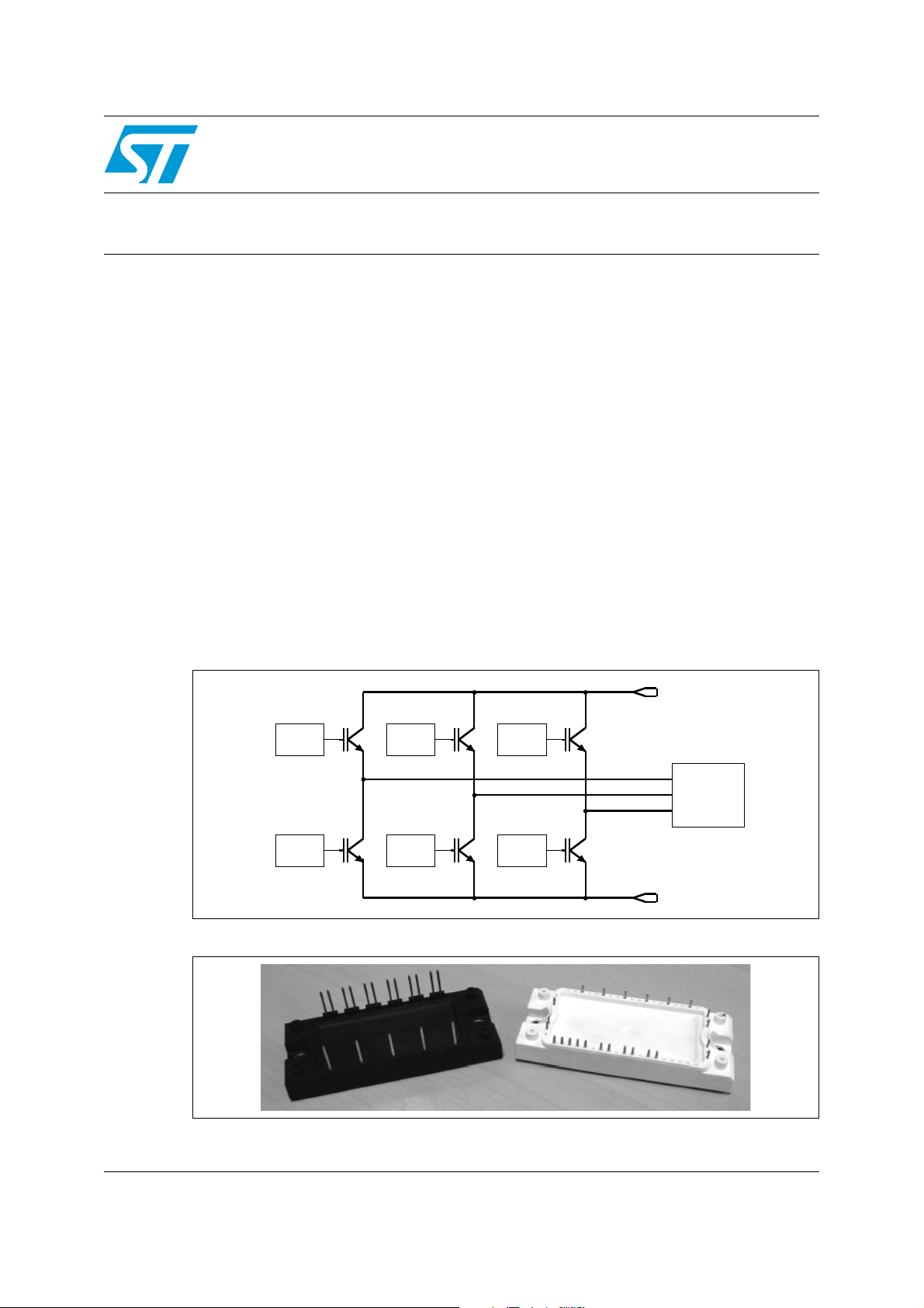
Applications include a three-phase full-bridge inverter used for motor speed control and
UPS systems.
TD350 in 1200V 3-phase inverter application
HV DC
TD350
TD350
TD350
TD350
TD350
Load
TD350
GND
IGBT modules
October 2006 Rev 4 1/21
www.st.com

Contents AN1944
Contents
1 TD350 application example . . . . . . . . . . . . . . . . . . . . . . . . . . . . . . . . . . . 3
2 Input stage . . . . . . . . . . . . . . . . . . . . . . . . . . . . . . . . . . . . . . . . . . . . . . . . . 4
3 Output stage . . . . . . . . . . . . . . . . . . . . . . . . . . . . . . . . . . . . . . . . . . . . . . . 5
4 Active Miller clamp . . . . . . . . . . . . . . . . . . . . . . . . . . . . . . . . . . . . . . . . . . 7
5 2-Level turn-off . . . . . . . . . . . . . . . . . . . . . . . . . . . . . . . . . . . . . . . . . . . . 10
6 Desaturation protection feature . . . . . . . . . . . . . . . . . . . . . . . . . . . . . . . 13
7 Application schematics . . . . . . . . . . . . . . . . . . . . . . . . . . . . . . . . . . . . . 15
8 Conclusion . . . . . . . . . . . . . . . . . . . . . . . . . . . . . . . . . . . . . . . . . . . . . . . . 19
9 Revision history . . . . . . . . . . . . . . . . . . . . . . . . . . . . . . . . . . . . . . . . . . . 20
2/21
AN1944 TD350 application example
L
1 TD350 application example
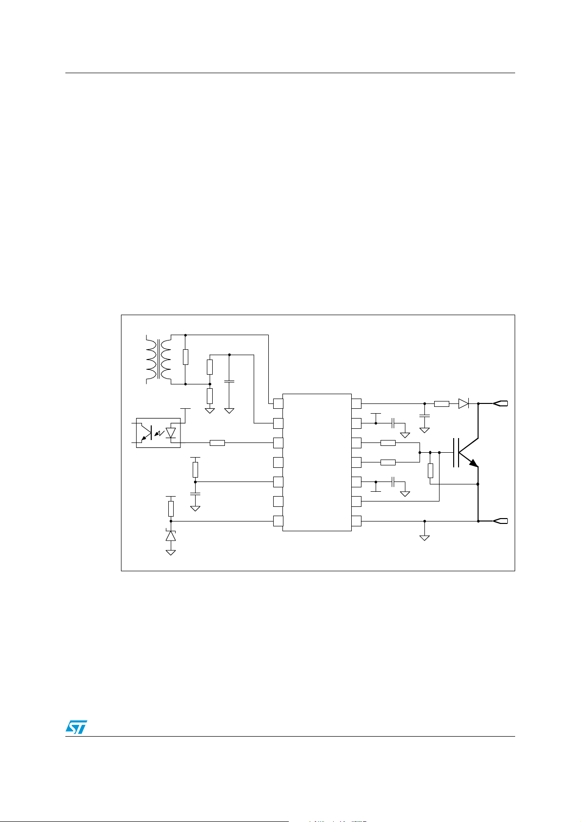
Figure 1 shows an example of a TD350 application where the device is supplied by a
+16V/-10V isolated voltage source, but a single voltage source can also be used. A pulse
transformer is used for input signal galvanic isolation. Gate resistors at OUTH and OUTL
pins (here 47 Ohms) are to be chosen depending on the IGBT specifications and the
manufacturer recommendations. Sink and source resistor values can be independently
tuned to optimize the turn-on and turn-off behaviors and can help to solve EMI issues.
The pull-down resistor (10kOhms in this example) connected between gate and emitter of
the external IGBT ensures that the external IGBT remains OFF during the TD350 power-up
sequence.
As the driver may be used in a very noisy environment, care should be taken to decouple
the supplies. The use of 100nF ceramic capacitors connected from VH to GND (and from VL
to GND if applicable) is recommended. The capacitors should be located as close as
possible to the TD350 and the ground loops should be reduced as much as possible.
Figure 1. TD350 application example showing all the features
VH
10K
11V
VH
10K
10K
10K
VREF
10K
4,7K
470pF
10nF
100pF
1kV
diode
1K
TD350
IN
1
VREF
2
FAULT
3
NC
4
COF F
5
NC
6
LVOFF
7
DESAT
VH
OUTH
OUT
CLAMP
GND
VL
14
16V
13
100nF
12
11
10
9
8
100nF
-10V
47R
47R
10K
3/21
Input stage AN1944
2 Input stage
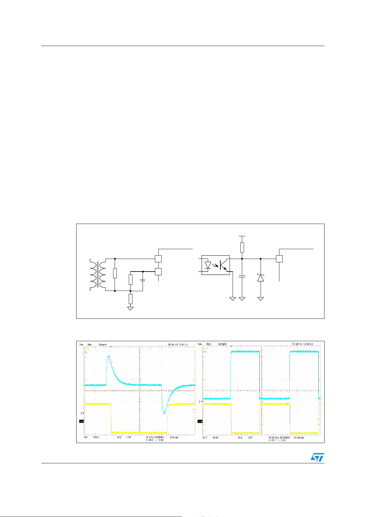
The TD350 is compatible with both pulse transformers or optocouplers. The schematic
diagram shown in Figure 2 can be considered as example of use with both solutions.
When using an optocoupler, the IN input must be limited to approximately 5V. The pull-up
resistor to VH must be between 5kOhms and 20kOhms, depending on optocoupler
characteristics. An optional filtering capacitor can be added in the event of a highly noisy
environment, although the TD350 already includes a filtering on input signals and rejects
signals smaller than 100ns (t
When using a pulse transformer, a 2.5V reference point can be built from the 5V VREF pin
with a resistor divider. The capacitor between the VREF pin and the resistor divider middlepoint provides decoupling of the 2.5V reference, and also ensures a high level on the IN
input pin at power-up to start the TD350 in OFF state.
specification).
ONMIN
The waveform from the pulse transformer must comply with the t
ONMIN
and V
tON/VtOFF
specifications. To turn ON the TD350 outputs, the input signal must be lower than 0.8V for at
least 220ns. Conversely, the input signal must be higher than 4.2V for at least 200ns to turn
OFF TD350 outputs. A pulse width of about 500ns at these threshold levels is
recommended. In all cases, the input signal at the IN pin must be between 0 and 5V.
Figure 2. Application schematic (pulse transformer: left / optocoupler: right)
VH
10K
10K
10K
10nF
10nF
TD350
IN
1
VREF
2
4K7
47pF
5,1V
TD350
IN
1
Figure 3. Typical input signal waveforms with pulse transformer (left) or
optocoupler (right)
4/21
AN1944 Output stage
3 Output stage
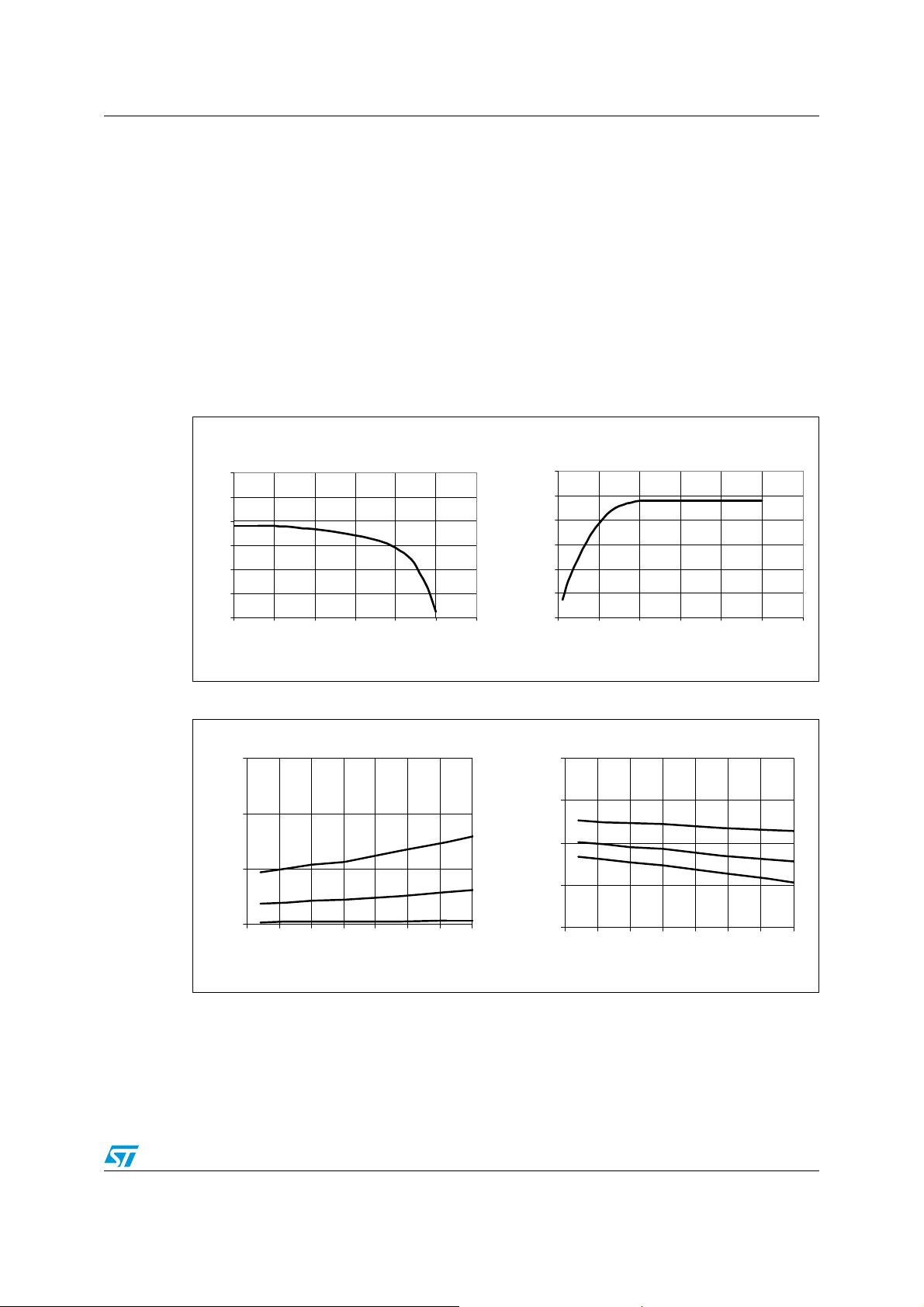
The output stage is able to sink/source about 2A/1.5A typical at 25°C with a voltage drop
V
OL/VOH
range (-20°C/+125°C) are 1.2A sink and 0.75A source. V
are guaranteed to 3V and 4V maximum respectively, over the temperature range (Figure 5).
This current capability sets the limit of IGBT driving, and the IGBT gate resistor should not
be lower than approximately 15Ω.
The TD350 uses separate sink and source outputs (OUTL/OUTH) for easy gate driving.
Output current capability can be increased by using an external buffer with two low-cost
bipolar transistors.
Figure 4. Typical output stage current capability at 25°C (VH = 16V, VL = -10V)
of 5V (Figure 4). The minimum sink/source currents over the full temperature
and VOH voltage drops at 0.5A
OL
OUT source curr ent versus voltage (turn -on)
3
2,5
2
1,5
Iout (A)
1
0,5
0
-10-5 0 5 101520
Vout (V)
OUT sink c urrent ver sus voltage (turn-off)
3
2,5
2
1,5
Iout (A)
1
0,5
0
-10-5 0 5 101520
Vout (V)
Figure 5. Typical VOL and VOH voltage variation with temperature
3.0
3.0
2.0
2.0
Iosink=500mA
Iosink=500mA
VOL -VL ( V)
VOL -VL ( V)
1.0
1.0
0.0
0.0
-50 -25 0 25 50 75 100 125
-50 -25 0 25 50 75 100 125
Temp (°C)
Temp (°C)
Iosink=200mA
Iosink=200mA
Iosink=20mA
Iosink=20mA
4.0
4.0
3.0
3.0
2.0
2.0
VH- VOH ( V)
VH- VOH ( V)
1.0
1.0
0.0
0.0
-50 -25 0 25 50 75 100 125
-50 -25 0 25 50 75 100 125
Temp (°C)
Temp (°C)
Iosource =500mA
Iosource =500mA
Iosource=2 00mA
Iosource=2 00mA
Iosource =20mA
Iosource =20mA
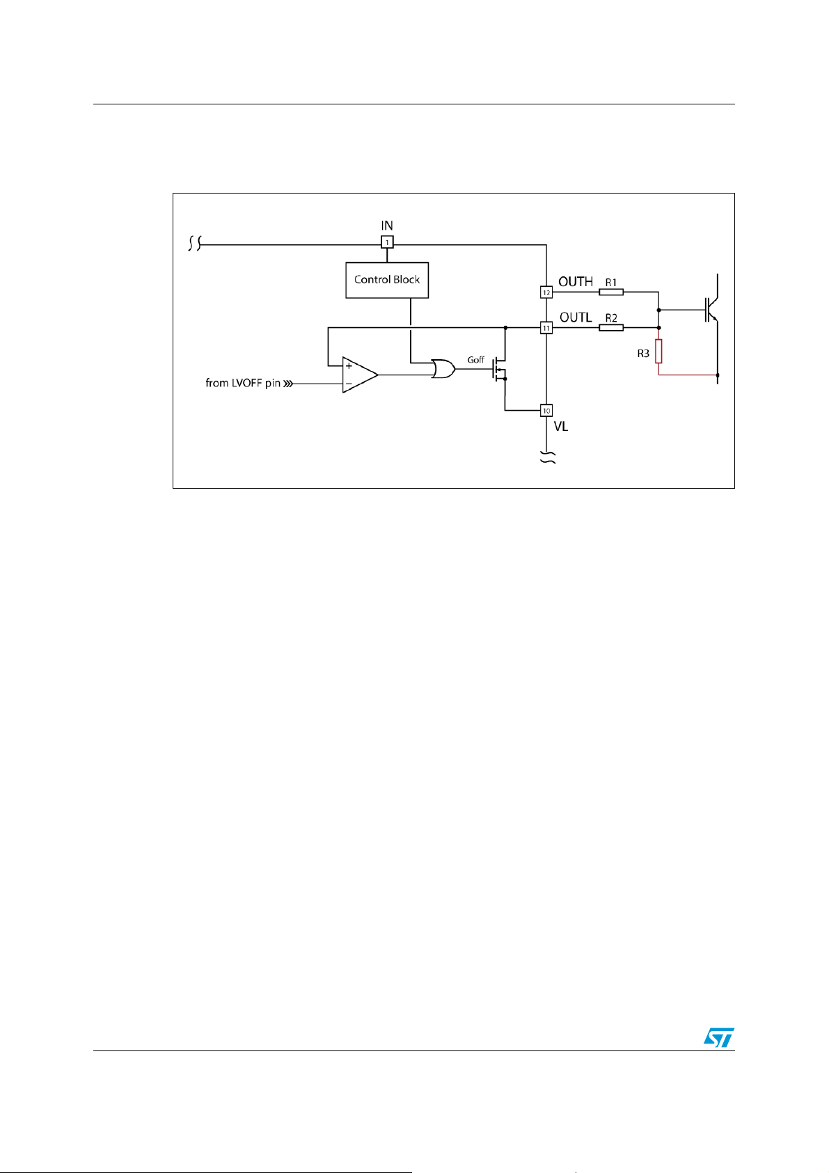
During the power-on sequence, it is not guaranteed that the Goff signal, which controls the
OUTL-MOS (see TD350 output stage schematic diagram in Figure 6), stays HIGH. In this
case when TD350 goes out from UVLO condition, the OUTL-MOS is turned off and OUTL is
in High-Impedance state until the first IN transition occurs. In these conditions some leakage
effects might slowly charge the external IGBT gate-emitter capacitance.
5/21
Output stage AN1944
Thus, it is recommended the use of a pull-down resistor of 10 kOhm or less (R3 in Figure 6)
connected between the gate and emitter of the external IGBT.
Figure 6. TD350 output stage schematic
6/21

AN1944 Active Miller clamp
4 Active Miller clamp
The TD350 offers an alternative solution to the problem of the Miller current in IGBT
switching applications. Instead of driving the IGBT gate to a negative voltage to increase the
safety margin, the TD350 uses a dedicated CLAMP pin to control the Miller current. When
the IGBT is off, a low impedance path is established between IGBT gate and emitter to carry
the Miller current, and the voltage spike on the IGBT gate is greatly reduced (see Figure 7).
The CLAMP switch is opened when the input is activated and is closed when the actual gate
voltage goes close to the ground level. In this way, the CLAMP function doesn’t affect the
turn-off characteristic, but only keeps the gate to the low level throughout the off time. The
main benefit is that negative voltage can be avoided in many cases, allowing a bootstrap
technique for the high side driver supply.
The waveform shown in Figure 8 proves how using the Active Miller clamp provides a
consistent reduction of the voltage spike on IGBT gate.
Figure 7. Active Miller clamp: principle of operation
TD350
Miller current Miller current
high dV/ dt !
active clamp
vol tage spi ke on IGB T gat e !
high dV/ dt !
reduce d volt age spik e
7/21

Active Miller clamp AN1944
Figure 8. Reduction of gate voltage spike by active Miller clamp
without Miller clamp
Vgs spike higher than 3V!
Miller clamp implemented
in the same conditions,
the Vgs spike is reduced to less than 1V
For high power applications, a buffer can be used at the CLAMP pin, in the same way as at
the driver output. Figure 9 shows a schematic principle with external buffers for both the
driver output and the CLAMP function.
Figure 9. Using external buffer to increase the current capability of the driver and
CLAMP outputs
TD350
13
12
11
10
9
8
VH
OUTH
OUTL
VL
CLA MP
GND
VH
T1
T2
T3
For very high-power applications, the Active Clamp function cannot replace the negative
gate drive, due to the effect of the parasitic inductance of the Active Clamp path. In these
cases, the application can benefit from the CLAMP output as an secondary gate discharge
path (see Figure 10).
When the gate voltage goes below 2V (i.e. the IGBT is already driven off), the CLAMP pin is
activated and the gate is rapidly driven to the negative voltage. Again, the benefit is to
improve the time to drive IGBT with large gate capacitance to the low level without affecting
the IGBT turn-off characteristics.
8/21

AN1944 Active Miller clamp
Figure 10. CLAMP used as secondary gate discharge path in large power
applications
TD350
VH
13
OUTH
12
OUTL
11
VL
10
CLAMP
9
GND
8
Caution: What to do with the CLAMP pin when not used?
Connect the CLAMP pin to VL.
VH
T1
T2
VL
T3
VL
9/21

2-Level turn-off AN1944
5 2-Level turn-off
In the event of a short-circuit or over-current in the load, a large voltage overshoot can occur
across the IGBT at turn-off and can exceed the IGBT breakdown voltage. By reducing the
gate voltage before turn-off, the IGBT current is limited and the potential over-voltage is
reduced. This technique is called a 2-level turn-off. Both the level and duration of the
intermediate off-level are adjustable. Duration is set by an external resistor/capacitor in
conjunction with the integrated voltage reference for accurate timing. The level can be easily
set by an external Zener diode, and its value is selected depending on the IGBT
characteristics. This 2-level turn-off sequence takes place at each cycle; it has no effect if
the current does not exceed the normal maximum-rated value, but protects the IGBT in case
of over-current (with a slight increase of conduction losses).
This principle is shown on Figure 11. During the 2-level turn-off time, the OUTL output is
controlled by a comparator between the actual OUTL pin and an external reference voltage.
When the voltage on OUTL goes down as a result of the turn-off and reach the reference
threshold, then the OUTL output is disabled and the IGBT gate is not discharged further.
After the 2-level turn-off delay, the OUTL output is enabled again to end the turn-off
sequence.
To keep the output signal width unchanged relative to the input signal, the turn-on is delayed
by the same value as the 2-level turn-off delay (Figure 12).
Figure 11. Principle schematic for 2-level turn-off feature
VREF
VH
5
7
COFF
2,5V
LVOFF
120µA
Control
Block
Lvof f off
OUTL
VL
11
10
The duration of the 2-level turn-off is set by the external RC components, and is given by the
formula:
Equation 1
tAµs[] 0.7 R
off
KΩ[]• C
off
nF[]•=
For example: With R
Recommended values are R
=10kΩ and C
off
off
=220pF, tA delay is approximately 1.5 microseconds.
off
from 10kΩ to 20kΩ, and C
a range of delay from approximately 0.7 to 4.6 microseconds.
10/21
from 100pF to 330pF, providing
off

AN1944 2-Level turn-off
Figure 12. Waveforms of the 2-level turn-off function (COFF timing exaggerated for
illustration)
IN input
COFF timing
OUTH/L outputs
Tests with an IGBT module of 1200V and 25A (Eupec FP25R12KE) are shown in Figure 13
for a 150A over-current event.
– Classical turn-off: OUT voltage is turned-off from VH = 16V to VL = -10V
– 2-level turn-off: OUT voltage is turned-off from VH = 16V to LVOFF = 11V during
1.5µs and ultimately OUT is pulled to VL = -10V
The maximum voltage reached on the IGBT collector and commutation losses are shown in
Ta bl e 1 for both nominal rated current at 25°C (40A) and over-current (150A) conditions.
There is no noticeable difference at nominal current, and the over-voltage is greatly reduced
in case of over-current event.
Figure 13. Reduction of IGBT over-voltage stress using 2-level turn-off feature
Without 2-level turn-off
Vce max reaches 1000V!
2-level turn-off implemented
Vce max is reduced t o 640V
11/21

2-Level turn-off AN1944
Table 1. Comparison between classical turn-off and 2-level turn-off
400V/40A 400V/150A
Turn-off mode
Eoff (mJ) Vce max(V) Eoff (mJ) Vce max (V)
Classical turn-off 2.5 620 15 1000
2-level turn-off with LVoff = 11V 2.5 620 23 640
Caution: How does one disable the 2-level turn-off feature?
Connect LVOFF to VH, remove C
4.7kΩ to 10kΩ resistor.
capacitor and keep COFF pin connected to Vref by a
off
12/21

AN1944 Desaturation protection feature
6 Desaturation protection feature
The desaturation function provides a protection against over-current events. Voltage across
the IGBT is monitored, and the IGBT is turned off if the voltage threshold is reached. A
blanking time is made of an internal 250µA current source and an external capacitor. The
high voltage diode blocks the high voltage during IGBT off state (a standard 1kV or more
diode is usable); the 1kΩ (approx.) resistor filters parasitic spikes and also protects the
DESAT input (see Figure 14).
During operation, the DESAT capacitor is discharged when TD350 output is low (IGBT off).
When the IGBT is turned on, the DESAT capacitor starts charging and desaturation
protection is effective after the blanking time (t
Equation 2
tB7.2 V[]
Equation 3
µs[] 0.03 Cdes at pF[]•=
t
B
When a desaturation event occurs, the fault output is pulled down and TD350 outputs are
low (IGBT off) until the IN input signal is released (high level), then activated again (low
level).
).
B
Cdesat
----------------------
•=
250 µA[]
Figure 15 shows a desaturation fault at 150A on a typical 25A module.
Figure 14. Application schematic for DESAT feature
TD350
VH
10K
FAULT
3
Control
Block
250µA
7,2V
DESAT
14
GND
8
100pF
1kV
diode
1K
Vce
Note that during half-bridge commutation, the DESAT pin can experience a voltage peak. It
can depend proportionally to the parasitic capacitante (Cj) of the desaturation diode, to the
voltage value of the DC bus and in inverse proportion to the value of the capacitance placed
on the DESAT pin and to the value of the resistor in series with the desaturation diode. The
voltage peak on the DESAT pin must not exceed the absolute maximum rating indicated in
the TD350 datasheet.
13/21

Desaturation protection feature AN1944
Figure 15. The collector current ramp-up to 150A triggers the DESAT feature (test on
25A module)
Caution: What should one do with the DESAT pin when it is not used?
Connect the DESAT pin to GND.
14/21

AN1944 Application schematics
7 Application schematics
The TD350 application designs presented below are based on the Active Miller clamp
concept. With this function, the high-side driver can be supplied with a bootstrap system
instead of using a floating positive/negative supply (see Figure 15). This concept is
applicable to low and medium power systems, up to approximately 10kW. The main benefit
of this is to reduce the global application cost by making the supply system simpler.
Figure 16 shows the half-bridge design concept using the TD350.
It should be highlighted that the Active Miller clamp is fully managed by the TD350 and does
not require any special action from the system controller.
Figure 16. TD350 application concept
5
Rb
24V
15V
+
Cb 4.7u
15V
Vreg
15k
15k
IN
IN
high side
TD350
TD350
VH
OUT
VL
CLAMP
VH
OUT
VL
CLAMP
The TD350 is able to drive 1200V IGBT modules up to 50A or 75A (depending on IGBT
technology and manufacturer). Key parameters to consider are the TD350 peak output
current (0.75A source / 1.2A sink) and the IGBT gate resistor.
The values of gate resistors should be chosen starting with the recommended values from
the IGBT manufacturer. The TD350 allows different values for source and sink. Thanks to
the Active Miller clamp function, the gate resistors can be tuned independently from the
Miller effect that normally put some constraints on the gate resistor. The benefit of this is the
optimization of turn-on and turn-off behavior, especially regarding switching loses and EMI
issues. Tab le 2 shows the recommended gate resistors values from two major IGBT module
manufacturers, and the peak gate current (with a 15V supply) required for 10A to 100A IGBT
modules. Approximate application power is indicated.
15/21

Application schematics AN1944
Table 2. Recommended gate resistors
Application power 1.5 2 3 4 3 7 11 15 [kW]
Eupec: FPxxR12KE3 15 25 40 50 75 [A]
Rgate 75 36 27 18 5 [Ohm]
Ipeak 0.2 0.4 0.55 0.8 3 [A]
Fuji: 6MBIxxS-120 10 15 25 35 50 75 100 [A]
Rgate 120 82 51 33 24 16 12 [Ohm]
Ipeak 0.12 0.2 0.3 0.45 0.6 0.9 1.3 [A]
IGBT modules suitable for the TD350 are indicated in bold. For the FP50R12KE3 and
6MBI75S-120 modules, the source (charging) peak current will be limited to 0.75A in worstcase conditions instead of the theoretical 0.8A or 0.9A peak values, this usually does not
affect the application performance.
An external buffer will be required for higher power applications.
Reference schematics are shown in Figure 17 and Figure 18. Both use the bootstrap
principle for the high-side driver supply. A very simple voltage regulator is used in front of the
TD350 high-side driver. In this way, the bootstrap supply voltage can be made significantly
higher than the target driver supply, and the voltage across the bulk capacitor (C
) can
B
exhibit large voltage variations during each cycle with no impact on the driver operation.
Gate resistors RgL and RgH depend on the IGBT. It should be noted that the applications
only use two supplies referenced to the ground level.
The application in Figure 17 uses desaturation detection for protection in case of overcurrent. Fault feedback is not used.
The application in Figure 18 uses the two-level turn-off function (level = 11V, duration =
1.5µs) instead of desaturation detection, with the benefit of saving a high voltage diode and
avoiding a connection to the IGBT collector.
It may be useful to use both methods together. In this case, just add the components for
desaturation detection together with the 2-level turn-off schematic diagram.
16/21

AN1944 Application schematics
Figure 17. TD350 application schematic diagram with desaturation protection
5
5
5
24V
15V
4.7u
high side drivers
2.2k
16V
5.1V
15k
IN
10n
VREF
FAULT
10k
TD350
COFF
DESAT
VH
OUTH
OUTL
VL
1k
100p
100n
RgH
RgL
CLAMP
100n
+
15k
LVOFF
IN
10n
5.1V
VREF
FAULT
10k
TD350
COFF
GND
DESAT
VH
OUTH
OUTL
VL
1k
100p
100n
RgH
RgL
CLAMP
LVOFF
GND
low side drivers
17/21

Application schematics AN1944
Figure 18. TD350 application schematic diagram with 2-level turn-off
24V
5
5
5
15V
4.7u
high side drivers
2.2k
16V
5.1V
15k
IN
10n
VREF
FAULT
10k
10k
TD350
COFF
DESAT
VH
OUTH
OUTL
VL
100n
RgH
RgL
CLAMP
100n
+
15k
5.1V
LVOFF
220p
11V
IN
10n
VREF
FAULT
10k
10k
TD350
COFF
GND
DESAT
VH
OUTH
OUTL
VL
100n
RgH
RgL
CLAMP
GND
11V
LVOFF
220p
18/21
low side drivers

AN1944 Conclusion
8 Conclusion
The TD350 is a versatile device designed for 1200V, 3-phase inverter applications,
especially for motor control and UPS systems. It covers a large range of power applications,
from 0.5kW to more than 100kW.
Thanks to its Active Miller clamp feature and low quiescent current, it can help avoid using
negative gate driving for applications up to 10kW and simplifies the global power supply
system for cost-sensitive applications.
19/21

Revision history AN1944
9 Revision history
Table 3. Revision history
Date Revision Changes
09-Sep-2004 1 Initial release
03-May-2006 2
26-Sept-2006 3
09-Oct-2006 4 -Figure 2. modified
- Quality of drawings improved according to A. Boimond remark.
- AN reviewed according to CCD comments
- New template
- Minor editing changes
20/21

AN1944
Please Read Carefully:
Information in this document is provided solely in connection with ST products. STMicroelectronics NV and its subsidiaries (“ST”) reserve the
right to make changes, corrections, modifications or improvements, to this document, and the products and services described herein at any
time, without notice.
All ST products are sold pursuant to ST’s terms and conditions of sale.
Purchasers are solely responsible for the choice, selection and use of the ST products and services described herein, and ST assumes no
liability whatsoever relating to the choice, selection or use of the ST products and services described herein.
No license, express or implied, by estoppel or otherwise, to any intellectual property rights is granted under this document. If any part of this
document refers to any third party products or services it shall not be deemed a license grant by ST for the use of such third party products
or services, or any intellectual property contained therein or considered as a warranty covering the use in any manner whatsoever of such
third party products or services or any intellectual property contained therein.
UNLESS OTHERWISE SET FORTH IN ST’S TERMS AND CONDITIONS OF SALE ST DISCLAIMS ANY EXPRESS OR IMPLIED
WARRANTY WITH RESPECT TO THE USE AND/OR SALE OF ST PRODUCTS INCLUDING WITHOUT LIMITATION IMPLIED
WARRANTIES OF MERCHANTABILITY, FITNESS FOR A PARTICULAR PURPOSE (AND THEIR EQUIVALENTS UNDER THE LAWS
OF ANY JURISDICTION), OR INFRINGEMENT OF ANY PATENT, COPYRIGHT OR OTHER INTELLECTUAL PROPERTY RIGHT.
UNLESS EXPRESSLY APPROVED IN WRITING BY AN AUTHORIZED ST REPRESENTATIVE, ST PRODUCTS ARE NOT
RECOMMENDED, AUTHORIZED OR WARRANTED FOR USE IN MILITARY, AIR CRAFT, SPACE, LIFE SAVING, OR LIFE SUSTAINING
APPLICATIONS, NOR IN PRODUCTS OR SYSTEMS WHERE FAILURE OR MALFUNCTION MAY RESULT IN PERSONAL INJURY,
DEATH, OR SEVERE PROPERTY OR ENVIRONMENTAL DAMAGE. ST PRODUCTS WHICH ARE NOT SPECIFIED AS "AUTOMOTIVE
GRADE" MAY ONLY BE USED IN AUTOMOTIVE APPLICATIONS AT USER’S OWN RISK.
Resale of ST products with provisions different from the statements and/or technical features set forth in this document shall immediately void
any warranty granted by ST for the ST product or service described herein and shall not create or extend in any manner whatsoever, any
liability of ST.
ST and the ST logo are trademarks or registered trademarks of ST in various countries.
Information in this document supersedes and replaces all information previously supplied.
The ST logo is a registered trademark of STMicroelectronics. All other names are the property of their respective owners.
© 2006 STMicroelectronics - All rights reserved
STMicroelectronics group of companies
Australia - Belgium - Brazil - Canada - China - Czech Republic - Finland - France - Germany - Hong Kong - India - Israel - Italy - Japan -
Malaysia - Malta - Morocco - Singapore - Spain - Sweden - Switzerland - United Kingdom - United States of America
www.st.com
21/21
 Loading...