

Page 1
AN1941
APPLICATION NOTE
LOW VOLTAGE LED DRIVER USI N G
L6920D, L4971 AND L6902D
1 INTRODUCTION
High brightness LE Ds are becoming a pr ominent sou rce of li ght and often have be tter eff iciency and reliability when compared to that of conventional light sources. While LEDs can operate from an energy source as simple as a battery and resistor, most applications require an
efficient e nergy sour ce not onl y for t he red uction of l osses, bu t als o for the l umen mainten ance
of the LED itself. STMicroelectronics has developed the following non-isolated DC-DC constant current LED driver to aid designers in developin g a low cost and efficient pl atform for dri ving high brightnes s LEDs.
This application note will cover 3 DC-DC power supplies to drive high intensity LEDs.
1 The L6920D boost converter to drive 1 LED for a flash lig ht application
2 The L4971 buck converter to dr ive 1 to 9 LEDs
3 The L6902D buck converter to dr ive 1 to 6 LEDs
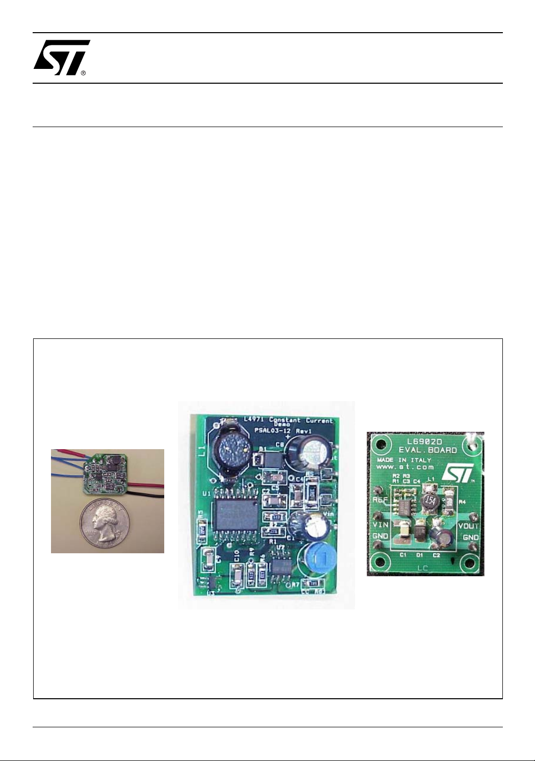
Figure 1. Reference Design Boards:
AN1941/0604
L6920D L4971 L6902D
1/15
Page 2
AN1941 APPLICATION NOTE
2 L6920D LED DRIVER
White LEDs are gaining popularity as sources of illumination because of their high efficiency
and reliabili ty. Typical forwar d volt age dr op of a wh ite LED i s appr oximat el y 3.5V. When these
LEDs are power ed fr om a singl e or two cell batt erie s, a boos t convert er i s needed t o boost the
voltage to drive the LEDs.
2.1 L6920D Descripti on
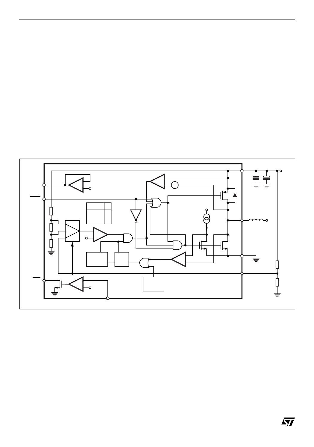
L6920D is a hig h efficiency step-up converter requiring very few ext e rnal components to realize the conversio n from the batt ery voltag e to the selected output volt age or curren t. The startup is guaranteed at 1V and the device i s operating down to 0.6 V. The device has very low qui escent current, only 10µA. Internal synchronous rectifier is implemented with a 120mΩ Pchannel MOSFET, replaci ng the convent ional boos t diode, to impro ve the effi ciency. This al so
implies a reduced cost in the application since no external diode required.
Following is the block diagr am of L6920D.
Figure 2. Block diagram of L6920D
V
OUT
V
IN
V
REF
SHDN
LBO
OUT
ZERO CROSSING
+
VBG
FB Y
V
OUT
A
GND
B
R
C
+
Y
VBG
1,R2
-
+
Toff min
1µsec
VBG
OPAMP
(CR)
LBI
RQS
A
B
C
Ton max
5µsec
+
- +
CURRENT LIMIT
VOUT
LX
+
GND
FB
D99IN1041
In L6920D, the control is based on the comparator that continuously checks the status of the
feedback signal. If the feedback voltage is lower than reference value, the control function of
the L6920D directs the energy stored in the inductor to be transferred to the load. This is accomplished by alternating between two basic steps:
– Ton phase: the botto m MOFSET Q1 is t urn ed on, an d the i nduc tor is c harg ed. The s wit ch
is turned off if the current reaches 1A or after a maximum on-time set to 5s.
– Toff phase: the bottom MOSFET Q1 is turned off, a nd top MOSFET Q2 is turned on. The
energy stored in the inductor is transferred to the load for at least a minimum off time of
1s. After this, the synchronous switch is turned off as soon as the feedback signal goes
lower than reference or the current flowing in the inductor goes down to zero.
2/15
Page 3
AN1941 APPLICATION NOTE
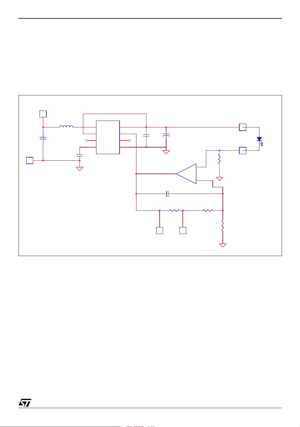
2.2 Circuit Description
The circuit shown in fi gure 3 is a constant current control to provide constant luminosity from
the LED. A current sensing res istor is in series with the white LED is used to provi de the current
feedback. Th e feedback r eference voltage for the controller i s 1.23V. If this voltage level is directly feedback from the current sensing resistor, the loss in the resistor will be too high. The
circuit uses a low value se nse re sist or, R1 to reduce t he dissi pati on and an op-amp to ampl ify
the current sense vol tage back up to the required 1.23V level.
Figure 3. Schematic of L6920D LED driver
J2
J6
CON1
CON1
L1
1
C2
10 uH
+
47uF
6.3V
1
U1
7
LX
5
SHDN
2
LBI
4 6
REF GND
L6 920
C4
.1u F
OUT
LBO
J4
R1
.33 O hm
1 2
1/4W
1
1
CON1
J5
CON1
D1
LED
8
.47uF
+
C5
C1
47uF
6.3V
OPAMP
U2 TS95 1ILT
+
OUT
-
1
FB
3
C3
.01uF
From the circuit, the control rule is: I
where I
is the current through the LED; R1 is the current sensing resistor, K is the gain of
LED
·R1·K = Vref
LED
1
J7
CON1
R2
1 2
100K
1/8W
1
J8
CON1
R3
1 2
12K
1/8W
R4
1K
1/8W
1 2
the OP AMP, and Vref is the reference voltage.
V
REF
Therefore, the LED current will be
I
LED
----------------=
R1 K⋅
In the reference ci rcuit, there are two gains. When J7 and J8 ar e shorted, K1= 1+R3/R4. When
J7 and J8 are open, K2=1+(R3+R2) /R4.
In the circuit, R1 = 0.33Ω; R2 = 100 kΩ; R3 = 12 kΩ; R4 = 1 kΩ. the current level of the LED
can be I
= 280mA or I
LED1
LED2
= 32 mA.
Following are some typical waveforms at Vin=2.5 V.
3/15
Page 4
AN1941 APPLICATION NOTE
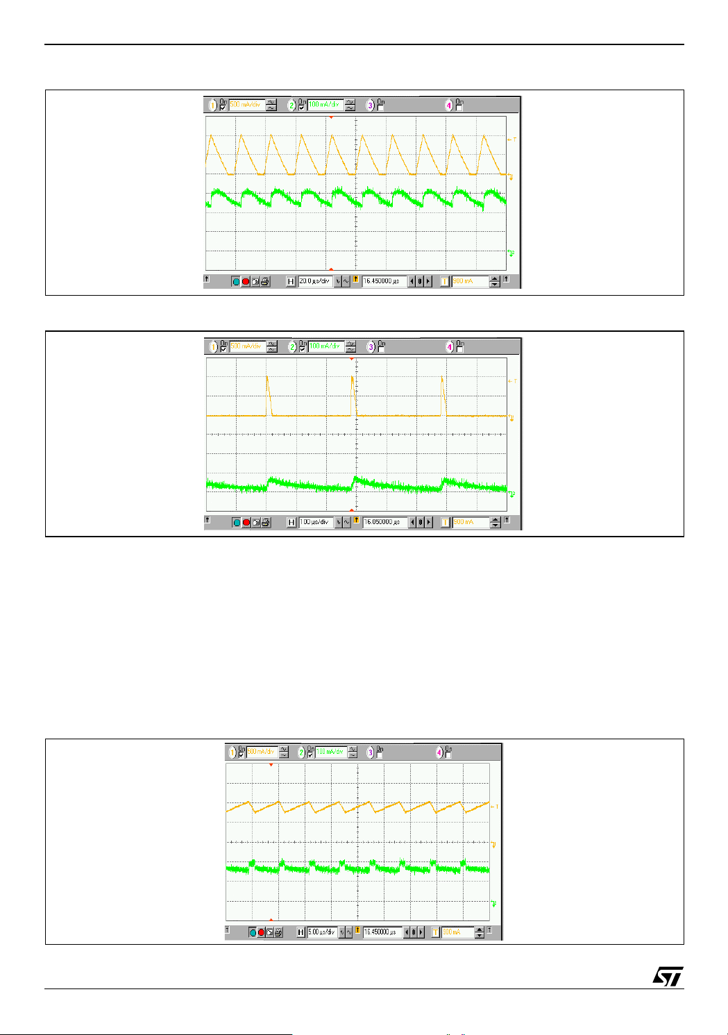
Figure 4. Upper trace: inductor current; lower track: LED current
500mA/div
I
L
100mA/div
I
LED
Figure 5. Upper trace: inductor current; lower track: LED current
500mA/div
I
L
100mA/div
I
LED
from the waveforms, the inductor peak current is limited at 1A. the maximum load current is
defined by following relationship:
I
load_lim
where η is the efficiency, I
=1A, and T
lim
When the load is heavier than I
Vin
-------------
Vout
load_lim
I
T
lim
offmin
off min
=1µs.
, the regulation will be lost, an d the inductor current will
Vout Vin–
-----------------------------
⋅
2L⋅
η⋅–⋅=
go to continuous mode. Fig. 6 and Fig. 7 show that the circui t loses th e regulatio n, but the circuit is running at its maximum duty cycle.
Figure 6. Vin = 1V; upper trace: inductor current; lower trace: LED current
500mA/div
500mA/div
I
I
L
L
100mA/div
100mA/div
I
I
LED
LED
4/15
Page 5
AN1941 APPLICATION NOTE
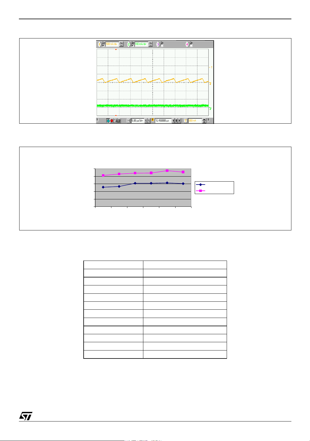
Figure 7. Vin = 0.6V; upper trace: inductor current; lower trace: LED current
500mA/div
I
L
100mA/div
I
LED
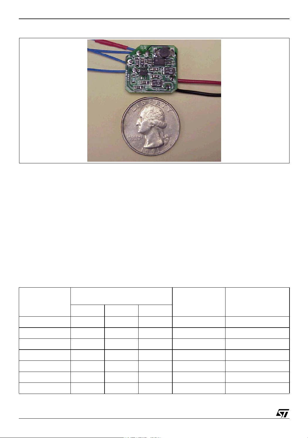
Fig. 8 shows the efficiency of the driver at dif ferent load and input voltages.
Figure 8. Efficiency curve
Efficiency
1
0.9
0.8
0.7
0.6
Efficiency (%)
0.5
1.92.12.32.52.7 3
Input Voltage (V)
275mA Output
30mA Output
Table 1. Bill of Material :
C2,C1 47uF 6.3V Electro sm
C3 .47uF 0805
C4 .1uF 0805
C5 .01uF 0805
L1 10uH sm inductor
R1 .33 Ohm 1% 1/4W 0805
R2 100K 5% 0805
R3 12K 5% 0805
R4 1K 5% 0805
U1 L6920D Tssop8
U2 TS951ILT sot23
Ref Value
5/15
Page 6
AN1941 APPLICATION NOTE
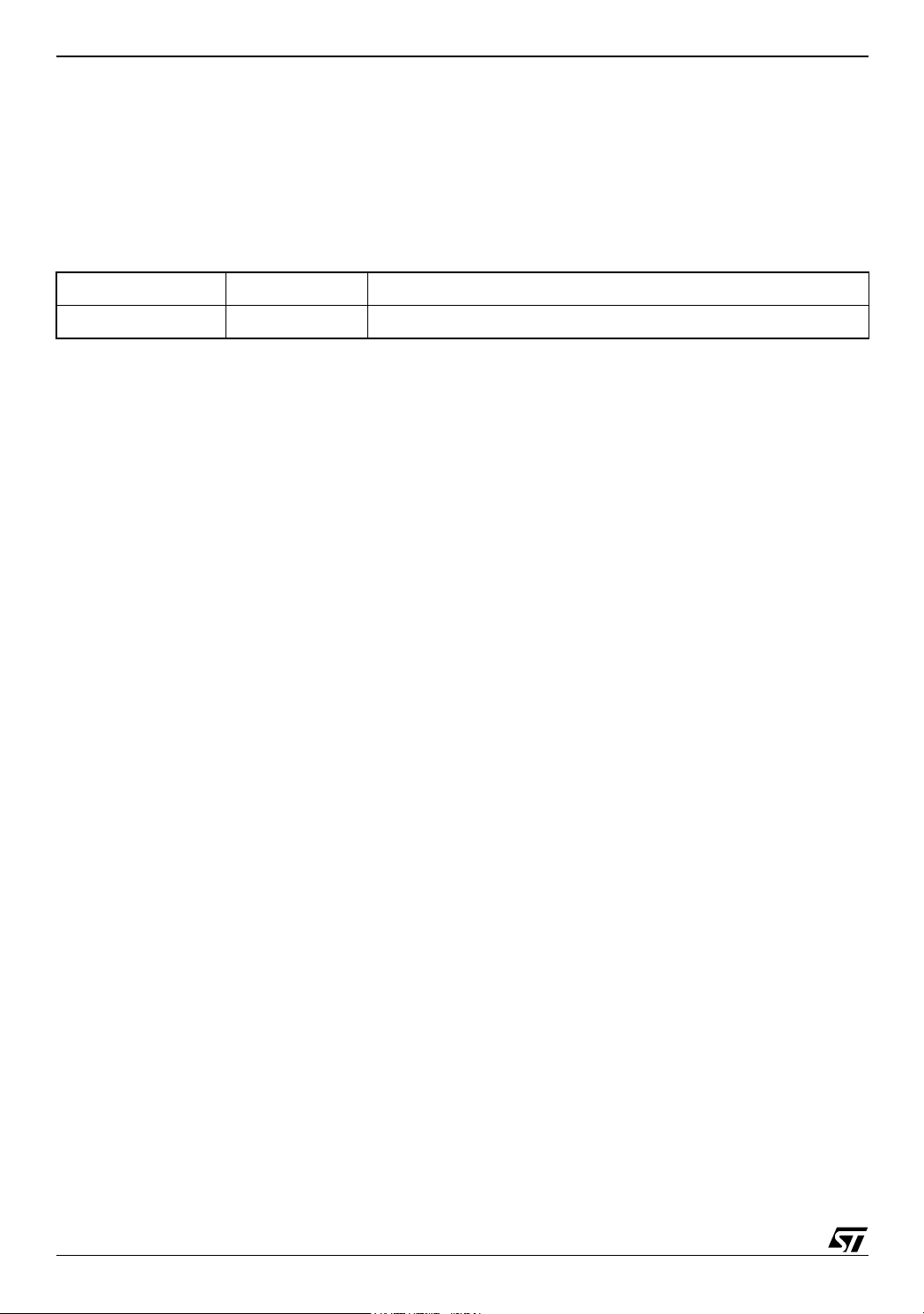
Figure 9. Size of the demo board
3 L4971 BUCK LED DRIVER:
For applicati ons that use multiple LEDs it is better to drive LEDs in series rather than parallel.
3.1 LED parameters;
As shown below, the LED volta ge drop tolerance varies by ±16.6% for the whit e LED. Different
colors will have dif ferent typical voltage drop. For t his reason, it is recommended that the LEDs
be connected in series rather than parallel. If connected in parallel, the current would not be
shared equally b etwe en the mul tipl e LEDs due to the di ffer ences i n forwar d v oltage dro p. Different brightn ess would resul t depending on individua l voltage drop of the string of LEDs. With
the LEDs connect ed in ser ies t he same curren t fl ows thro ugh ea ch LED and t he out put wi ll be
better matched.
Below is the forward voltage drop spec sheet from Luxeon Star Technical Data Sheet DS23
Table 2.
Forward Voltage
(V)
V
Color
Min. Typ. Max.
White 2.79 3.42 3.99 1.0 -2.0
Green 2.79 3.42 3.99 1.0 -2.0
Cyan 2.79 3.42 3.99 1.0 -2.0
Blue 2.79 3.42 3.99 1.0 -2.0
Royal Blue 2.79 3.42 3.99 1.0 -2.0
F
Dynamic
Resistance
(Ω) R
D
T emperature Coefficient
of Forward Voltage
(mV/°C)
∆V
/∆T
F
J
6/15
Red 2.31 2.85 3.27 2.4 -2.0
Amber 2.31 2.85 3.27 2.4 -2.0
Page 7

AN1941 APPLICATION NOTE
The brightness is directly proportional to the current driving the LED. A test was conducted i n
a closed box with a white LED mounted 12 inches away from the light meter. The results
showed a linear relationship between current and light output. The graph in figure 2.3 also
shows the relation between current and forward drop of the LED.
When driving LEDs from a DC-DC buck topology the minimum voltage input that the power
supply will operate, the maximum voltage i nput and the maximum power capability of the unit
must be taken int o account. Tab le 2.2 shows t he capability o f the L4971 and L 6902D reference
designs for minimum input vo ltage and the maximum input voltage.
Table 3.
Control V in # LEDs Current
L6902D 8 1 350mA
L6902D 25 6 350mA
L4971 20 5 220-400mA
L4971 55 9 220-400mA
Figure 10.
3.2 L4971 LED Driver
The L4971 is a step down monolithic power switching regulator able to deliver 1.5A. Its construction i s BCD mixed technol ogy using an internal D-MOS t ransistor with low Rdson t o obtain
high efficiency and high switching speeds. Features of this DC-DC converter are pulse by
pulse curr ent l imit ; hi cc up mode fo r sho rt cir cuit p rotect ion, vol tage f eed for ward, sof t star t and
thermal shutdown. Typically it is used for regulating an output voltage. An output current can
also be regulated by sensing the voltage drop across a sense resistor, Rs as shown on the
following schematic.
7/15
Page 8

AN1941 APPLICATION NOTE
Figure 11.
3.3 Circuit description:
The input ranges from 20 vol ts to 55 volts. The switching frequency is set by
1
6
-- -
5
100 C
⋅+ln⋅
osc
where R
osc
and C
F
SW
represent R2 and C2.
osc
-------------------------------------------------------------------------------=
R
oscCosc
The minimum volta ge for the L4 971 is 8 volts but the regu lator-ref erence U3 needs a minimum
of 20 volts to stay in regulation. A higher breakdown voltage regulator can be used to achieve
a wider range of input. U3 provides power to the LM393 and a reference for the comparator
input. This vo ltage is compared t o the voltag e drop across Rs to mai ntain it at t he same voltage
set by the poten tiomet er R8. Th e v oltage drop acr oss t he res isto r is propor tio nal t o the cur rent
following through it by:
Iout = V(U2Apin3)/Rs.
The output of the LM 393 turns on and off to adjust the voltage at the slow start pin. The slow
start voltage is directly related to the output regulation thus achieving a constant current output. The L4971 regulates by adjusting the duty cycle to maintain a constant output. R9 set s
the gain o f the loop by c ontroll ing the discharg e rate. L1 and C8 form the o utput fil ter to smooth
out the current. The inductor required is calculated at the worse case which is max input line
and minimum LEDS. This gives the minimum duty cycle and maximum time that the i nductor
has to suppl y current to the load.
D
max
VoVf+
-----------------------------
V
+
in minVf
D
min
VoVf+
-----------------------------
V
+
in minVf
L
VoVf+()
o
1D
–()
min
---------------------------
⋅===
I
⋅∆
ofsw
is the current ripple set by the application, usually 10% of the max current.
∆I
o
8/15
Page 9

AN1941 APPLICATION NOTE
R3 and R4 set the maximum voltage to 30 volts. R8 will adjust the constant curren t output from
220 mA to 400 mA.
I
Table 4. Part List
tem Qty Ref Part Tolerance Description
1 1 C1 39u 63V P10339-ND
2 1 C2 1nF 50V sm ce ramic
3 1 C4 22nF 50V sm ceramic
4 1 C5 1u 25V sm PCC1893CT
5 1 C6 0.1u 50V sm ceramic PCC1893CT
6 1 C7 220nF 50V sm ceramic
7 1 C8 100u 35V P10294
8 2 C9,C10 0.1u sm ceramic
9 1 D1 STPS160U ST
10 1 D3 1N5242A 12V zener
11 1 L1 470uH Coilcraft DO3316P-474
12 1 RS 1 1/2W sm 2510
13 1 R1 9.1k
14 2 R9,R2 51k
15 1 R3 8.2k
16 1 R4 1k
17 1 R5 15k
18 1 R6 13k
19 1 R7 560
20 1 R8 500 36G52-ND
21 1 U1 L4971 ST
22 1 U2 LM393D ST
23 1 U3 LD2979_sot23-5 ST
The output voltage can be changed by readjusting the resistor divider R3 and R4 to allow a
higher output voltage to drive as many as 15 LEDs of typical forward volta ge drop.
3.4 Results:
With a minimum in put vol tage of 20 V, u p to 5 LEDs can be d riven and wi th 33 V to 55 V i nput,
9 LEDs can be driven limited by the output voltage set at 30 volts.
9/15
Page 10

AN1941 APPLICATION NOTE
Figure 12. Current regulation:
The current regulation is ± 1% for the range of 1 to 9 LEDs or a voltage range of 3.3 volts to
29 volts output.
Figure 13. Efficiency at 55V input:
The efficiency differences shown in figure 13 are primarily related to differences in the output
power. As the numbe r of LEDs increa ses, the output power also i ncrease s. However, the los ses in the system remain r elati vely co nstant over the r ange so the effici ency in cre ases with the
number of LEDs.
Figure 14. Ripple current
10/15
Page 11

AN1941 APPLICATION NOTE
4 L6902D BUCK LED DRIVER:
Another buck topology reference design that is much simpler, less expensive and requires
fewer external compon ents is the L6902D LED driver. The f eatures of the L6902D are:
4.1 L6902D Descripti on
– Up to 1A of output current
– Input voltage from 8V to 36V
– Built in 5% output current accura cy
– 250KHz internall y fixed frequency
– Adjustable current limit
– Thermal shut down
The L6902D is a complete and simple step down switching regulator with adjustable constant
voltage and constant current. By means of a current sense resistor set to give a 0.1V drop
across it, the current ca be set to any desired value up to 1 amp. Iout=0.1V/Rsen se.
Figure 15. Internal Block Diagram:
The L6902D contai ns a vol tage a nd a c urr ent er ror ampl ifi er wi th an i nt ernal r efer ence of 3.3V
and 1.235 with a tolerance of ±2%. Most of the external circuits of the previous design are incorporated inside this battery charger chip. This 8 pin chip mini mizes pin count by fixing the
switching fr equency and allowing 2 pins for current sensing, 1 for sensing the output voltage .
11/15
Page 12

AN1941 APPLICATION NOTE
Figure 16. Schematic
R4a
6.2
1W
R4
.30
1W
I=350 mA up to 23.2V
1
R1
4.7K
R2
240
Vout
+
C2
47uF
25V
GND out
1
Vin=8 to 25V
1
GND in
1
C1
10uF
25V
C3
220pF
C4
22nF
R3
5.1K
U1
L6902D
8
Vcc
6
Vref
4
Comp
1
Out
2
CS+
3
CS-
5
FB
Gnd
7
0
L1
150uH
D1
STPS340U
4.2 Circuit description:
The IC can operate up to 36 volts. The 25 volt input capacitor was the restr icting factor for the
input and o utput voltage. More LEDs can be driven i f a 35 volt cap is used for C1 and C2. C3,
C4, and R3 stabilize the feedback loop. R1 and R2 set the output voltage limit to 23.2 volts,
below the rating of the output capacitor. D1 recirculates the current when the internal 250mΩ
P-channel DMOS transistor is turned off. R4, 0.3 ohms 1% standard resistor, sets the current
to 330mA. R4a, 6.2 ohms tweaks it to 350mA for the precise industry standard. L1 is det ermined as shown in the Table 4.
Table 5. BOM:
Qty Ref Part Voltage Cat #
1 C1 10uF 25V PCC2243CT
1 C2 47uF 25V P10267
1 C3 220pF PCC221BVCT
1 C4 22nF PCC2283CT
1 D1 STPS340U ST STPS340U
1 L1 150uH 350ma MOS-6020-154MXB
1 R1 4.7K P3.9KGCT
1 R2 240 P240GCT
1 R3 5.1K P5.1KGCT
1 R4 .30 1W 71-WSL2010-0.332
1 R4a 6.2 1W 71-WSL2010-0.332
1 U1 L6902D ST L6902D
12/15
Page 13

AN1941 APPLICATION NOTE
4.3 Results:
With a minimum of 8 volt s, 1LED can be dri ven and with the maxi mum of 25 volts, up t o 6 LEDs
can be driven.
Figure 17. Current regulation
The current regulat ion from 1 to 6 LEDs or 3.3V to 19.5V is ± 1.5%.
Figure 18. Efficiency at 25V input:
The efficiency ranges from 80% to 90% for 2 LEDs or more.
Figure 19. Ripple current
Peak to peak output rippl e current is less than 7% of the output current.
13/15
Page 14
AN1941 APPLICATION NOTE
5 CONCLUSION :
This application note has shown three reference designs to drive LEDs in constant current
mode. One is a boost, to drive a flashli ght at a higher voltage than the input. The others are
two buck topology to drive string in series for a various number of LEDs.
Table 6. Revision History
Date Revision Description of Changes
June 2004 1 First Issue
14/15
Page 15

AN1941 APPLICATION NOTE
The present note which is for guidance only, aims at providing customers with infor mation regarding their products in
order for them to save time. As a result, STMicroelectronics shall not be held liable for any direct, indirect or
consequential damages with respect to any claims arising from the content of such a note and/or the use made by
customers of the information contained herein in connection with their products.
Information furnished is believed to be accurate and reliable. However, STMicroelectronics assumes no responsibility for the consequences
of use of such inf orma tio n nor for any i nfr inge ment of pa tent s or oth er ri ght s of thi rd pa rti es wh ich m ay re sul t fr om it s use . No li cense is granted
by implica tio n o r ot he rw is e un d er a ny pa te nt o r pa te nt righ ts of S TM ic ro el ec tro nic s. Sp ec ific at io ns m e nt ion ed in this pu bl ica tion are subject
to change without notice. This publication supersedes and replaces all information previously supplied. STMicroelectronics products are not
authorized for use as critical components in life support devices or systems without express written approval of STMicroelectronics.
The ST logo is a registered trademark of STMicroelectronics.
All other names are the property of their respective owners
© 2004 STMicroelectronics - All rights reserved
Australia - Belgium - Brazil - Canada - China - Czech Republic - Finland - France - Germany - Hong Kong - India - Israel - Italy - Japan -
Malaysia - Malta - Morocco - Singa pore - Spain - Sweden - Switzerland - United Kingdom - United States
STMicr oe le ct ron ic s GR O U P OF CO MP A NI ES
www.st.com
15/15
 Loading...