

Page 1

AN1934
Obsolete Product(s) - Obsolete Product(s) Obsolete Product(s) - Obsolete Product(s)
®
- APPLICATION NOTE
VIPower: VIPer12A NON ISOLATED FLYBACK
CONV ERTE R RE FE R EN CE BO AR D
P. LIDAK - R. HAUSER
ABSTRACT
Presented circuit can be used to produce multiple outputs, non isolated pos itive or negat ive voltage. It is
dedicated for building an auxiliary power supply based on the VIPer12AS monolithic device.
1. INTRODUCTION
The aim of the presented reference boards is to propose a solution of the power supply based on an offline discontinuous current mode flyback converter without isolation between input and output. The
flyback topology allows to fully exploit current capability of the incorporated monolithic device VIPer12AS
when compared with buck converter based power s uppl y. To ensure low cost of the whole power supply
the isolation between input and output is not provided. This greatly simplifies the transformer design and
production. The VIPer12AS incorporates the PWM controller with 60 kHz internal oscillator and
altogether with the vertical power MO SF ET sw itch in a S O-8 package. T he presented power supply has
four variants. All these variants have been incorporated in presented reference board by different
assembly options.
2. CIRCUIT DESCRIPTION
2.1 NON ISOLATED FLYBACK +5V/500MA, +15V/200MA (VARIANT 1)
2.1.1 Operating Conditions
Input Voltage range
Input Voltage Frequency range
Main Output (regulated)
Second Output
Total Maximum Output Power
2.1.2 Circuit Operation
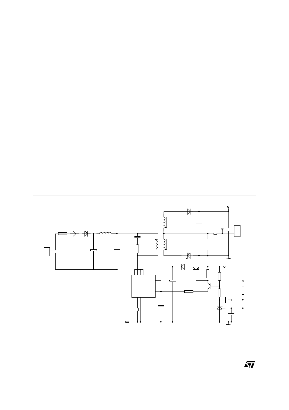
The total schematic of the power supply (Variant 1) can be seen in figure 1. The output of the converter is
not isolated from input. For this reason the reference ground is common for an input and output
connection terminal. The input capacitor C1 is charged from the mains by single rectification consisting
of diodes D1 and D2. Two diodes in series are used for EMI reasons to sustain burst pulses of 2kV. The
capacitor C1 together with capacitor C2 and inductor L1 form an EMI filter.
The DC voltage at C2 is then applied to the primary winding of the transformer through the internal
MOSFET switch of VIPer12 d uring ON time of the switching period. The s nubber circuit consisting of
resistor R3 and capacitor C6 red uces the voltage spike across the primary winding of the transformer
due to the parasitic leakage inductance. It al so slows down dV/dt of the primary winding’s voltage a little
bit and thus improves EMI.
The power supply provides two out puts from two transformers‘ windings through rectifiers D4, D5 and
smoothing capacitors C3 and C4. The VIPer12AS is supplied by 15V output voltage through transistor
90-264 VAC
50/60 Hz
5V / 500mA
15V 200mA
5.5W
April 2004 1/24
Page 2
Obsolete Product(s) - Obsolete Product(s) Obsolete Product(s) - Obsolete Product(s)
AN1934 - APPLICATION NOTE
Q2 and diode D7. The diode D7 ensures the proper start-up of the converter by separating the 15V
output from the internal start-up current source of the VIPer12AS which will charge the IC supply
capacitor C5 to a specified start-up threshold voltage of about 16V. As soon as C5 voltage reaches the
start-up thr eshold t he interna l 60 kHz o scillator se ts the int ernal flip- flop and tu rns on the i nternal h igh
voltage power MOSFET through the output driver. The power MOSFET applies the bul k capacitor C1
and C2 high voltage to the transformer’s primary winding a nd primary current will ramp-up. As soon as
the primary current ramp reaches the VIPer’s internal set-point defined by feedback loop, the internal
power switch turns off. The output capacitor C3 or C4 is charged by energy stored in the transformer
through rectifier diode D4 or D5. The current loop which charges the 5V output flows through diode D5
only. Because of the D5 location, the 15V output is charged via both diodes D4 and D5. Beside the slight
decrease of the conv erter power efficiency, it significantly im proves the cross-regulation of th e outputs
which was the main purpose of this arrangement.
The voltage feedback loop senses the 5V ou tput by resistor divider R5, R7. The c ontrol IC U2 compares
the resistor divider output voltage with internal reference voltage of 2.5V and changes the cathode
voltage accordingly to keep 5V output stable. If the 5V output voltage rises above it’s nominal value, the
cathode voltage of U2 g oes down and ca thode current will increase. The cathode current w ill cause a
voltage drop across R9 and opens transistor Q1 which will inject the current from Vcc line to FB pin 3 of
the VIPer12AS. The FB pin current will decrease the peak primary current to reduce the power delivered
to the outputs. Resistor R10 limits the U2 cathode current . Resistor R9 has two roles: it works as pull up
for Q1 and ensures bias current of at least 1mA for U2 proper operation.
Figure 1: Schematic diagram of non isolated flyback converter (variant 1)
R14
0R
C4
220uF
35V
LXY
R10
U2
+15V
CON2
3
+5V
2
1
clamp
+15V
R9
470R
1k
C9
100nF
C10
1nF
+5V
R5
4.7k
R8
4.7k
R7
4.7k
90...264V~
CON1
clamp
D1
R1
10R
GL1M
3W
1000V
L
1
2
N
1A
Layout Hints: C5, C8 have
to be close to VIPer12A
Assembly options:
(1): +5V/500mA, +15V/200mA
note: all voltages refer to
neutral
D2
GL1M
1000V
1A
C1
22uF
400V
KMG
L1
BC
330uH 190mA
+
C2
10uF
400V
KMG
D4
U1
15
56
4 3
VDDVDDVDDVDDVDDVDD
C5
10uF
4
50V
KME
3
FB
C8
22nF
EF16/4.7
AL = 120nH
Gap = 0.22mm
C6
100pF
500V
R16
0R
100R
R17
R3
0R
+
8
2
T1A
3.1mH
160 turns
0.18 CuLL
VDD
Drain15Drain26Drain37Drain4
Sour ce11Source2
VIPer12AS
T1B
33uH
16.5 turns
0.315 CuLL
T1C
10uH
9 turns
0.315 CuLL
D7
+
STPR120A
200V 1A
D5
STPS1L40A
40V 1A
LL4148
R11
4.7k
Q2
BC856B
BC856B
C3
+
120uF
35V
LXY
Q1
TS2431ILT
+
R2
4.7k
Resistor R11 limits the feedback current to a safe value, which is lower than specified by the maximum
rating table in the data sheet. Capacitor C8 improves noise immunity of the FB input against noise.
2/24
Page 3

Obsolete Product(s) - Obsolete Product(s) Obsolete Product(s) - Obsolete Product(s)
AN1934 - APPLICATION NOTE
2.1.3 Bill of materials
The bill of material presented in Table 1 covers all power supply variants. The components which are
specific for a particular variant can be recognized by column named "V ariant". Peak clamp D6 connected
across the primary winding is optional and it is not assem bled on the board. In case a precise voltage
regulation of the 15V output is required, resistor R6 connected from the 15V output to the control input of
U2 can be assembled instead of R5.
Table 1: Bill of material for all variants of non isolated flyback converter
Ref. Q.ty Variant Description
CON1 1
CON2 1
C1 1 22µF Electrolytic capacitor, Nippon Chemi-Con, KMG 400V, 20%
C2 1 10µF Electrolytic capacitor, Nippon Chemi-Con, KMG 400V, 20%
C3 1 120µF Electrolytic capacitor, Nippon Chemi-Con, LXY 35V 20%
C4 1 (1, 2, 4) 220µF Electrolytic capacitor, Nippon Chemi-Con, LXY 35V 20%
C5 1 10µF Electrolytic capacitor, Nippon Chemi-Con, KME 50V 20%
C6 1 100pF Ceramic capacitor, X7R, 500V C1206 10%
C8 1 22nF Ceramic capacitor, X7R, 50V C0805 10%
C9 1 (1, 4) 100nF Ceramic capacitor, X7R, 50V C0805 10%
C10 1 (1, 4) 1nF Ceramic capacitor, X7R, 50V C0805 10%
C11 1 (2)
(3)
D1, D2 2 GL1M Diode, Diotec, trr=1.5µs 1000V 1A, MiniMELF
D4 1 STMicroelectronics STPR120A Diode, fast recovery trr=25ns 200V 1A SMA
D5 1 (1, 2, 4)
(3)
D6 1 optional STMicroelectronics PKC-136 Diode, Peak clamp, Vbr=160V, 700V, 1.5W DO-15
D7 1 LL4148 Diode 75V 200mA
D8 1 (2, 3) ZMM13 Zener diode, 13V 0.5W 5%
L1 1 330µH Inductor, EPCOS, bobbin core, B78108-S1334-J, 190mA 6.4R 10%
Q1, Q2 2 (1, 4) BC856B Bipolar transistor, PNP, 65V 100mA 330mW
R1 1 10R resistor, Yageo, wirewound, fusible, TK120 CRF 254-4 3W 5%
R2, R5,
R7, R8
R3 1 100R resistor, metal film, 200V 0.25W R1206 1%
R4 1 (2, 3) 0R resistor, metal film, R1206
R6 1 optional 24K resistor, metal film, R0805, 100V 0.125W 1%
R9 1 (1, 4) 470R resistor, metal film, R0805, 100V 0.125W 1%
R10 1 (1, 4) 1K resistor, metal film, R0805, 100V 0.125W 1%
R17 1 0R resistor, metal film, R1206
T1 1 (1, 3, 4)
4 (1, 4) 4.7K resistor, metal film, 100V 0.125W R0805 1%
(2)
Clamp, WECO, 2 pole, horizontal, 1.5mm
Clamp, WECO, 3 pole, horizontal, 1.5mm
2.2µF Tantalum capacitor, Size A, B45196E, 10V 7.0R 20%
100nF Ceramic capacitor, X7R, 50V C1206 10%
STMicroelectronics STPS1L40A Diode, Schottky, 40V 1A, SMA
0R Resistor, metal film, R1206
Ns=16/9 turns transformer, Vogt, ferrite Fi324, EF16/4.7, ord. num. 545 23 249 00
Ns=14/11 turns transformer, Vogt, ferrite Fi324, EF16/4.7, ord. num. 545 23 249 00
2
, 380V, 15A
2
, 380V, 15A
3/24
Page 4
Obsolete Product(s) - Obsolete Product(s) Obsolete Product(s) - Obsolete Product(s)
AN1934 - APPLICATION NOTE
U1 1 STMicroelec tronics VIPer12AS, 730V 0.4A, 27R, f=60kHz, SO-8
U2 1 (1, 4) STMicroelectronics TS2431ILT shunt ref. IC, 2.5V 1mA to 100mA 360mW 2%
U3 1 (2)
(3b)
U4 1 (3a) STMicroelectronics L78M05CDT positive voltage reg., 5V, 0.5A 5%
2.1.4 Transformer Design
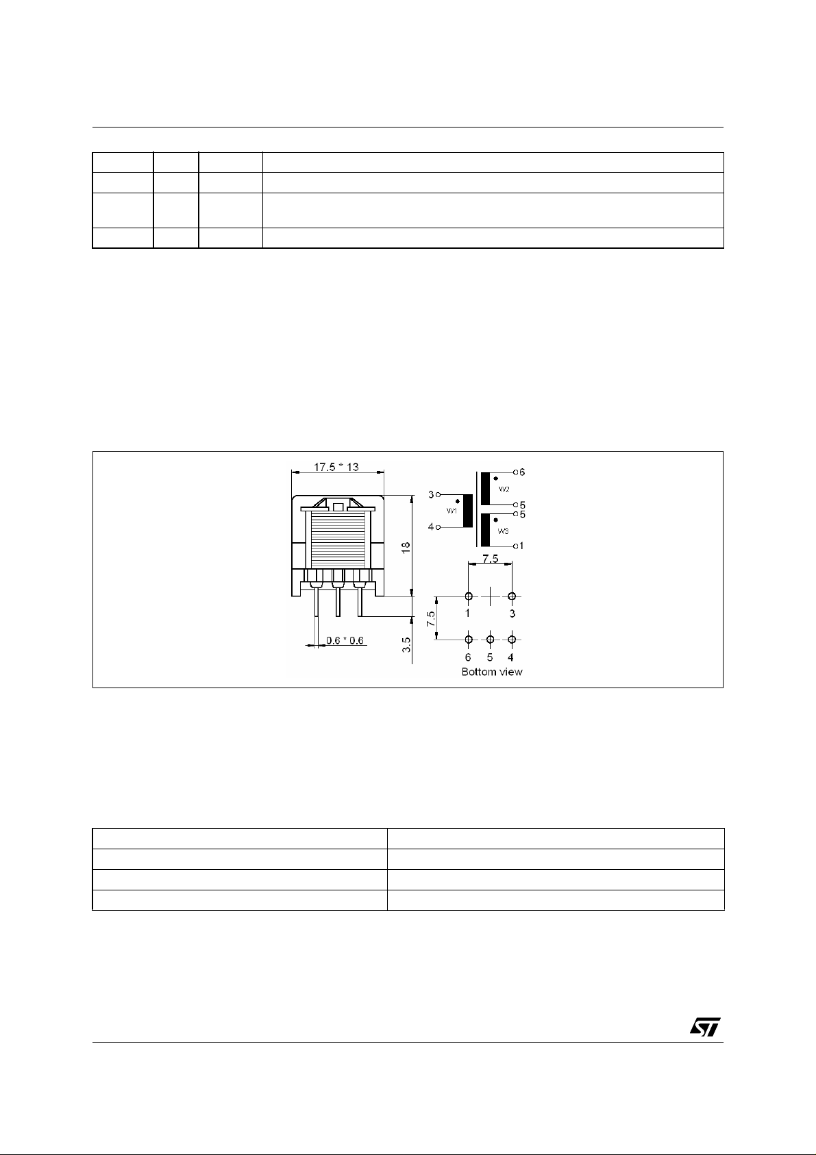
Since there is no requirement regarding isolation bet ween primary and sec ondary s ide, the t ransformer
construction is easier compared to the isolated version. There is only a single layer of Mylar tape
between the primary winding an d secondary windings. Its purpose is n ot to make transformer passing
safety regulations but to ensure proper operation of the power s uppl y. Also creepage distances between
windings are not that crit ical. T he physical appearance, dimensions and windin gs and pins arrangement
can be seen in figure 2.
Figure 2: Transformer dimensions, windings and bottom view pin arrangement
STMicroelectronics L4931CD50 voltage reg., low drop, with inhibit, 5V, 250mA 4%
STMicroelectronics L78L05CD positive voltage reg., 5V, 100mA 10%
The basic parameters of the ferrite core selected from Vogt’s ferrite materials and shapes can be seen in
table 2. The gap size was optimised to ensure appropriate current capability and inductance to fully
exploit switching frequency and to switch peak current limit of the VIPer12AS to achieve maximum output
power.
Table 2: Transformer’s core parameters
Shape
Material
Gap size [mm]
Inductance Factor AL [nH]
EF16/4.7
Vogt Fi 324
0.24
120
An overview of the most important parameters for each winding can be found in table 3. This table is valid
for all variants. The only differentiation between the variants is the num ber of turns for the secondary
windings. The difference is indicated in the "number of turns" column.
4/24
Page 5
Obsolete Product(s) - Obsolete Product(s) Obsolete Product(s) - Obsolete Product(s)
Table 3: Transformer’s windings parameters
AN1934 - APPLICATION NOTE
Order Start Pin End Pin No. of turns Wire
diameter [mm]
13 4
26 5
35 1
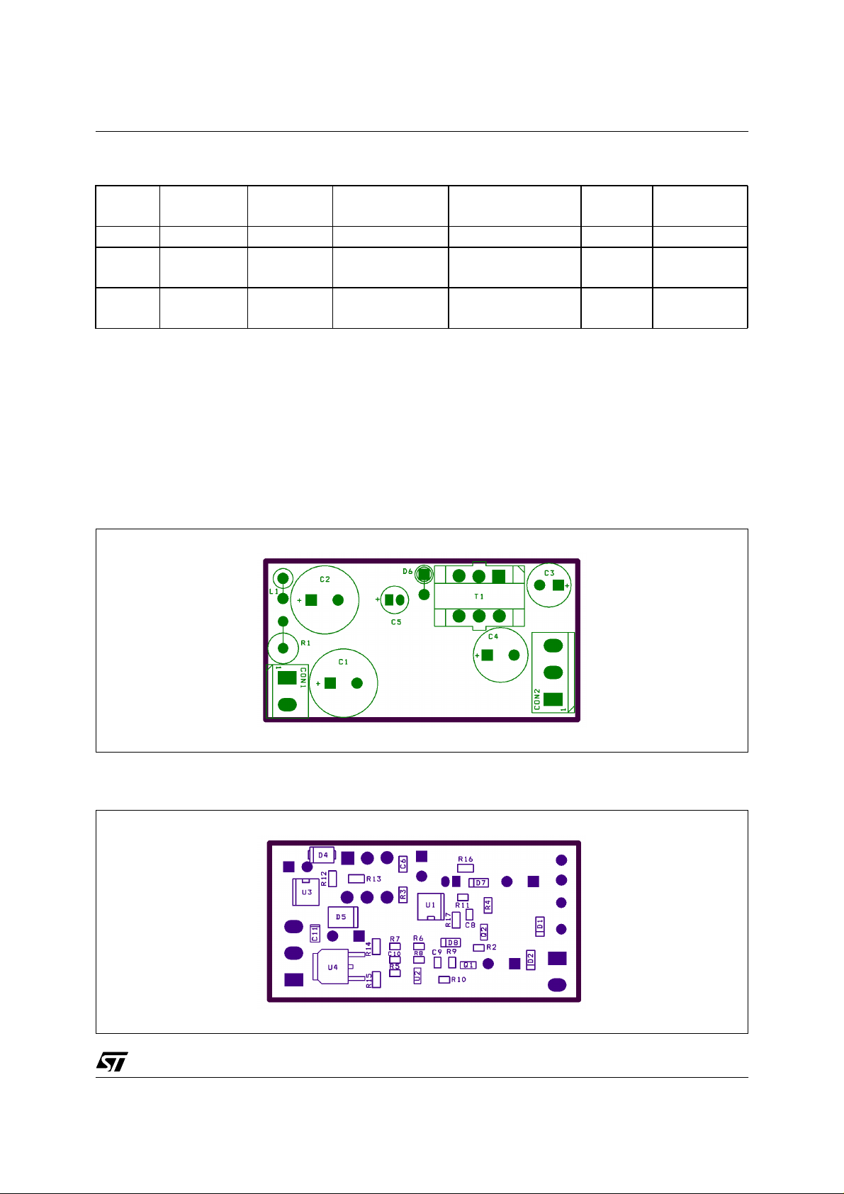
2.1.5 PCB Layout
The PCB is designed as a single sided board made of FR-4 material with 35µm copper plating with
solder and silk screen mask. The assembled board contains both SMD and through hole components.
The board includes all variants of the converter. The o utline dimensions are 59x30mm. Ass embly top
side (trough-hole components) and solder bottom (SMD com ponents) side can be s een in figure 3 and
fi gure 4.
Figure 3: Assembly Top (not in scale)
160
9 (1, 3, 4)
11 (2)
16.5 (1, 3, 4)
14.5 (2)
0.18 CuLL 3.1mH
0.315 CuLL 10µH
0.315 CuLL 33µH
Wire
material
Inductance
15µH
25µH
Figure 4: Assembly Solder Side (not in scale)
5/24
Page 6

Obsolete Product(s) - Obsolete Product(s) Obsolete Product(s) - Obsolete Product(s)
AN1934 - APPLICATION NOTE
The PCB layout of the copper connections is depicted in figure 5. The holes for through-hole components
are not seen in the picture.
Figure 5: PCB Layout (not in scale)
The physical appearance of the converter can be observed in figure 6.
Figure 6: Picture of the Converter
2.1.6 Evaluation and Measurements
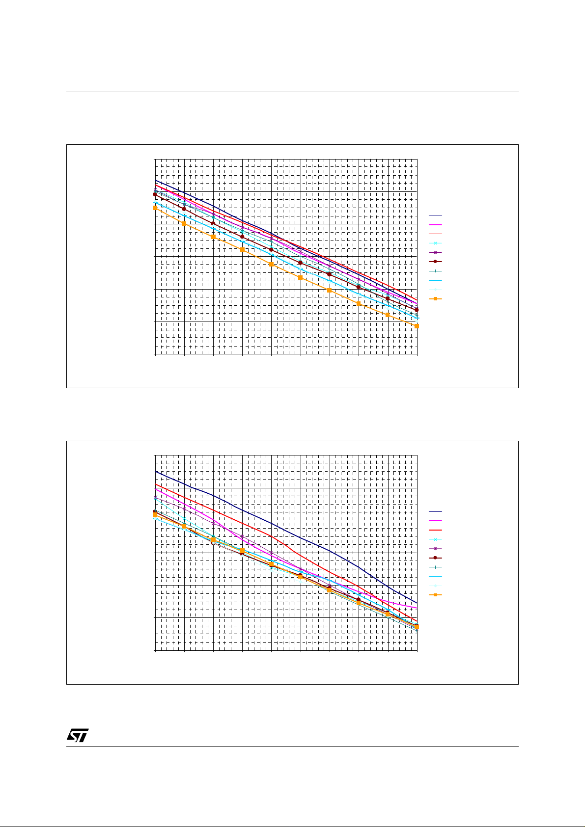
The output regulation characteristics measured on 5V output can be seen in figure 7. It shows the
voltage variation of the 5V output when different load is applied to 15V ou tput. Fi gure 8 s hows t he sam e
characteristic as figure 7 but measured at 375VDC input voltage.
6/24
Page 7
Obsolete Product(s) - Obsolete Product(s) Obsolete Product(s) - Obsolete Product(s)
AN1934 - APPLICATION NOTE
Figure 7: Output Regulation Cha racteristics of 5V output at 12 5VDC Input Voltage (Parameter is load
current on 15V output)
5.009
5.007
5.005
5.003
Output Voltage [V]
5.001
4.999
4.997
50 100 150 200 250 300 350 400 450 500
Out p ut Cu r r ent [A ]
20mA
40mA
60mA
80mA
100mA
120mA
140mA
160mA
180mA
200mA
Figure 8: Output Regulation Cha racteristics of 5V output at 37 5VDC Input Voltage (Parameter is load
current on 15V output)
5.009
5.007
5.005
5.003
Output Voltage [V]
5.001
4.999
4.997
50 100 150 200 250 300 350 400 450 500
Out p ut Cu r r ent [A ]
20mA
40mA
60mA
80mA
100mA
120mA
140mA
160mA
180mA
200mA
Similarly figure 9 shows the output regul ation characteristics measured on 15V output when different
7/24
Page 8
Obsolete Product(s) - Obsolete Product(s) Obsolete Product(s) - Obsolete Product(s)
AN1934 - APPLICATION NOTE
load current applied to 5 V output . Figure 10 shows the s ame cha racteristic as figu re 9 but measured at
375VDC input voltage.
Figure 9: Output Regul ation Characteristics of 15V Ou tput at 125VDC Input Voltage (Parameter is load
current on 5V output)
15.2
15
14.8
14.6
Output Voltage [V]
14.4
14.2
14
20 40 60 80 100 120 140 160 180 200
Output Current [A]
50mA
100mA
150mA
200mA
250mA
300mA
350mA
400mA
450mA
500mA
Figure 10: Output Regulation Characteristics of 15V Output at 375VDC Input Voltage (Parameter is load
current on 5V output)
15.2
15
14.8
14.6
Output Voltage [V]
14.4
14.2
50mA
100mA
150mA
200mA
250mA
300mA
350mA
400mA
450mA
500mA
14
20 40 60 80 100 120 140 160 180 200
Output Current [A]
8/24
Page 9

Obsolete Product(s) - Obsolete Product(s) Obsolete Product(s) - Obsolete Product(s)
AN1934 - APPLICATION NOTE
One of the most observed parameters when judging the converter performance is power efficiency.
Figure 11 depicts the dependency of the efficiency on load ap plied to the 5V output (parameter is l oad
current on 15V output). Similarly figure 12 shows the dependency on the 15V output current (parameter
is load current on 5V output). Figures 12 and 13 show t he same characteristics as figures 10, 11a and
11b, but measured at input voltage of 375 VDC.
Figure 11a: Efficiency vari ation with 5V Output Curren t at 125VDC Input Voltage (Parameter is loaded
current on 15V output)
80
75
20mA
40mA
60mA
70
Efficiency [%]
65
80mA
100mA
120mA
140mA
160mA
180mA
200mA
60
50 100 150 200 250 300 350 400 450 500
Output Current [mA]
Figure 11b: Efficiency variation wi th 15V O ut put Current at 125VDC Input Voltage (Parameter is loaded
current on 5V output)
80
75
50mA
100mA
150mA
70
Efficiency [%]
65
200mA
250mA
300mA
350mA
400mA
450mA
500mA
60
20 40 60 80 100 120 140 160 180 200
Output Curre nt [mA]
9/24
Page 10

Obsolete Product(s) - Obsolete Product(s) Obsolete Product(s) - Obsolete Product(s)
AN1934 - APPLICATION NOTE
Figure 12: Efficiency variation with 5V Output Current at 375VDC Input Voltage (Parameter is loaded
current on 15V output)
80
75
70
20mA
65
60
Efficiency [%]
55
50
45
50 100 150 200 250 300 350 400 450 500
Output Curre nt [mA]
40mA
60mA
80mA
100mA
120mA
140mA
160mA
180mA
200mA
Figure 13: Efficiency variation with 15V O utput Current at 375VDC Input Voltage (Parameter is loaded
current on 5V output)
80
75
70
50mA
65
60
Efficiency [%]
55
50
45
20 40 60 80 100 120 140 160 180 20 0
Figure 14 to figure 23 show the most important voltage or current waveforms at different input and output
conditions. Channel 1 (pi nk) is the power MO SFET Source te rminal voltage of the VIPer12. Ch annel 4
Output Current [mA]
100mA
150mA
200mA
250mA
300mA
350mA
400mA
450mA
500mA
(blue) shows the drain current of the VIPer12. The purpose of those pictures is to demonstrate the
skipping cycle function at light or no-load condition and cycle-by-cycle primary current limitation at output
shorted condition
10/24
Page 11

Obsolete Product(s) - Obsolete Product(s) Obsolete Product(s) - Obsolete Product(s)
AN1934 - APPLICATION NOTE
Figure 14: Vin=127VDC, no-load Figure 15: Vin=373VDC, no-load
Figure 16: Vin=127VDC, nominal load Figure 17: Vin= 373VDC, nominal load
Figure 18: V
=127VDC, 50% load on both outputs Figure 19: Vin=373VDC, 50% load on both outputs
in
11/24
Page 12

Obsolete Product(s) - Obsolete Product(s) Obsolete Product(s) - Obsolete Product(s)
AN1934 - APPLICATION NOTE
Figure 20: Vin=127VDC, 5V output shorted, 15V
output no-load
Figure 22: Vin=373VDC, 5V output shorted, 15V
output no-load
Figure 21: Vin=127VDC, 15V output shorted, 5V
output no-load
Figure 23: Vin=373VDC, 15V output shorted, 5V
output no-load
The feedback loop stability and reaction to the load change are demonstrated from figures 24 to 27.
12/24
Page 13

Obsolete Product(s) - Obsolete Product(s) Obsolete Product(s) - Obsolete Product(s)
AN1934 - APPLICATION NOTE
Figure 24: Load transient response, 50mA to
0.5A on 5V output, 15V output
unloaded, Vin=127VDC
Figure 26: Load transient response, 50mA to
0.5A on 5V output, 15V output
unloaded, Vin=373VDC
Figure 25: Load transie nt response, 50mA to
0.5A on 5V output, 15V output nominal
load, Vin=127VDC
Figure 27: Load transie nt response, 50mA to
0.5A on 5V output, 15V output nominal
load, Vin=373VDC
Furthermore, conducted emissions were measured in neutral and line wire using a peak or average
detector. The measurements were performed at 230VAC input voltage and both outputs were fully
loaded. The results can be seen from figures 28 to 31.
13/24
Page 14

Obsolete Product(s) - Obsolete Product(s) Obsolete Product(s) - Obsolete Product(s)
AN1934 - APPLICATION NOTE
Figure 28: Phase L, average detector Figure 29: Phase L, peak detector
Figure 30: Phase N, average detector Fi gure 31: Phase N, peak detector
2.2 NON ISOLATED FLY BACK +5V/250m A, +15V/ 200mA (VARIANT 2)
2.2.1 Operating Conditions
Input Voltage range
Input Voltage Frequency range
Main Output (regulated)
Second Output
Total Maximum Out pu t Power
14/24
90-264 VAC
50/60 Hz
15V / 200mA
5V / 250mA
4.25W
Page 15

Obsolete Product(s) - Obsolete Product(s) Obsolete Product(s) - Obsolete Product(s)
AN1934 - APPLICATION NOTE
2.2.2 Circuit Operation
The total schematic of the power supply can be seen in figure 32. Compared to variant 1, this variant has
some differences. The major difference is the feedback loop. Instead of 5V output the 15V output is
regulated by a simp le circuit consisting of zener diode D8 a res istor R11. Since 5V output is not well
stabilized by the feedback loop a linear regulator U3 is used. The linear regulator requires some input-tooutput voltage difference to assure a minimum dropout voltage. For this reason the number of turns of
secondary windings is slightly different compared to variant 1 (see table 3).
Figure 32: Schematic diagram of non isolated flyback converter (Variant 2)
D4
90...264V~
CON1
L
N
clamp
D1
GL1M
1000V
1A
D2
GL1M
1000V
1A
C1
22uF
400V
KMG
R1
10R
3W
L
1
2
N
Layout Hints: C5, C8 hav e
to be close to VIPer12A
Assembly options:
(2): +5V/250 mA, +15V/200mA
note: all voltages refer to neutral
L1
330uH 190mA
+
BC
C2
10uF
400V
KMG
T1A
VDD
15
56
4 3
U1
FB
VDD
C5
4
10uF
50V
KME
3
C8
22nF
EF16/4.7
AL = 120nH
Gap = 0.22mm
C6
100pF
500V
+
R16
0R
100R
R3
R17
0R
3.1mH
160 turns
0.18 CuLL
8
Drain15Drain26Drain37Drain4
Source 11Source 2
VIPer12AS
2
T1B
25uH
14.5 turns
0.315 CuLL
T1C
15uH
11 turns
0.315 CuLL
LL4148
+
D7
STPR120A
200V 1A
D5
STPS1L40A
40V 1A
R4
0R
R11
1k
2.3 NON ISOLATED FLYBACK +15V/200mA, +5V/60mA (VARIANT 3)
2.3.1 Operating Conditions
Input Voltage range
Input Voltage Frequency range
Main Output (regulated)
Second Output
Total Maximum Out pu t Power
C3
+
120uF
35V
LXY
+15V
D8
ZMM1 3
+
R13
0R
C4
220uF
35V
LXY
U3 L4931CD50
VIN8VOUT
4
90-264 VAC
50/60 Hz
15V / 200mA
5V / 20mA or 60mA
4.25W
+15V
CON2
3
+5V
1
GND36GND47GND23GND12NC25NC1
2
1
clamp
C11
+
2.2uF
10V
Ta
2.3.2 Circuit Operation
The schematic diagram is depicted in figure 33 and is very similar to the schematic of variant 2. It has
only one output rectifier diode and one o utput electrolytic capacitor. The 5V linear regulator is directly
supplied from 15V output . There are t wo sub-varia nts. Depending on the output current requiremen t for
5V output, U3 or U4 can be mounted.
15/24
Page 16

Obsolete Product(s) - Obsolete Product(s) Obsolete Product(s) - Obsolete Product(s)
AN1934 - APPLICATION NOTE
Figure 33: Schematic Diagram of Non Isolated Flyback Converter (Variant 3)
+5V
+15V
CON2
3
2
1
GND36GND47GND23GND12NC25NC1
1
clamp
C11
100nF
90...264V~
CON1
L
N
cl amp
D1
GL1M
1000V
1A
D2
GL1M
1000V
1A
C1
22uF
400V
KMG
R1
10R
3W
L
1
2
N
Layout Hints: C5, C8 have
to be close to VIPer12A
Assembly options:
(3a): +5V/60mA, +15V/200mA
(3b): +5V/20mA, +15V/200mA
note: all voltages refer to neutral
L1
330uH 190mA
+
BC
C2
10uF
400V
KMG
+15V
D4
15
STPR120A
T1B
56
VDD
C8
22nF
200V 1A
33uH
16.5 turns
0.315 CuLL
T1C
10uH
9 turns
0.315 CuLL
D7
LL414 8
C5
+
10uF
50V
KME
R11
C3
+
120uF
35V
D5
0R
1k
LXY
R4
+15V
0R
D8
ZMM13
EF16/4.7
AL = 120nH
Gap = 0.22mm
C6
100pF
500V
100R
+
R17
0R
R16
0R
T1A
3.1mH
160 tur ns
R3
0.18 CuLL
8
2
VDD
Drain15Drain26Drain37Drain4
Source11Source2
VIPer12AS
4 3
U1
4
3
FB
R12
(3b)
0R
U4 L78M05CDT
(3a)
VIN VOUT
GND
U3 L78L05CD (3 b )
VIN8VOUT
4
2.3.3 Evaluation and Measurements
The output regulation characteristics measured on 5V output can be seen in figure 34. It shows the
voltage variation of the 5V ou tput when a different load is applied to 15V output . Figure 35 shows the
same characteristic as figure 34 but measured at 375VDC input voltage.
Figure 34: Output Regulation Characteristics of 5V output at 125VDC Input Voltage (Parameter is
loaded current on 15V output)
5.013
5.011
5.009
5.007
5.005
5.003
5.001
4.999
4.997
Output Voltage [V]
4.995
4.993
4.991
4.989
4.987
6 1626364656
Output Current [A]
20mA
40mA
60mA
80mA
100mA
120mA
140mA
160mA
180mA
200mA
16/24
Page 17

Obsolete Product(s) - Obsolete Product(s) Obsolete Product(s) - Obsolete Product(s)
AN1934 - APPLICATION NOTE
Figure 35: Output Regulation Characteristics of 5V output at 375VDC Input Voltage (Parameter is
loaded current on 15V output)
5.012
5.010
5.008
5.006
5.004
5.002
5.000
4.998
4.996
Output V oltag e [ V ]
4.994
4.992
4.990
4.988
4.986
4.984
6 1626364656
Output Current [A]
20mA
40mA
60mA
80mA
100mA
120mA
140mA
160mA
180mA
200mA
Similarly, figure 36 shows the output regulation characteristics measured on 15V output when different
load current applied to 5V output. Figure 3 7 s hows the same characteristic as figure 36 but measured at
375VDC input voltage.
Figure 36: Output Regulation Characteristics of 15V Output at 125VDC Input Voltage (Parameter is
loaded current on 5V output)
15
14.8
14.6
Output Vo l tage [V ]
14.4
6mA
12mA
18mA
24mA
30mA
36mA
42mA
48mA
54mA
60mA
14.2
20 40 60 80 100 120 140 160 180 200
Output Current [A]
17/24
Page 18

Obsolete Product(s) - Obsolete Product(s) Obsolete Product(s) - Obsolete Product(s)
AN1934 - APPLICATION NOTE
Figure 37: Output Regulation Characteristics of 15V Output at 375VDC Input Voltage (Parameter is
loaded current on 5V output)
15.2
15
Output Voltag e [V]
14.8
14.6
20 40 60 80 100 120 140 160 180 200
Output Current [A]
6mA
12mA
18mA
24mA
30mA
36mA
42mA
48mA
54mA
60mA
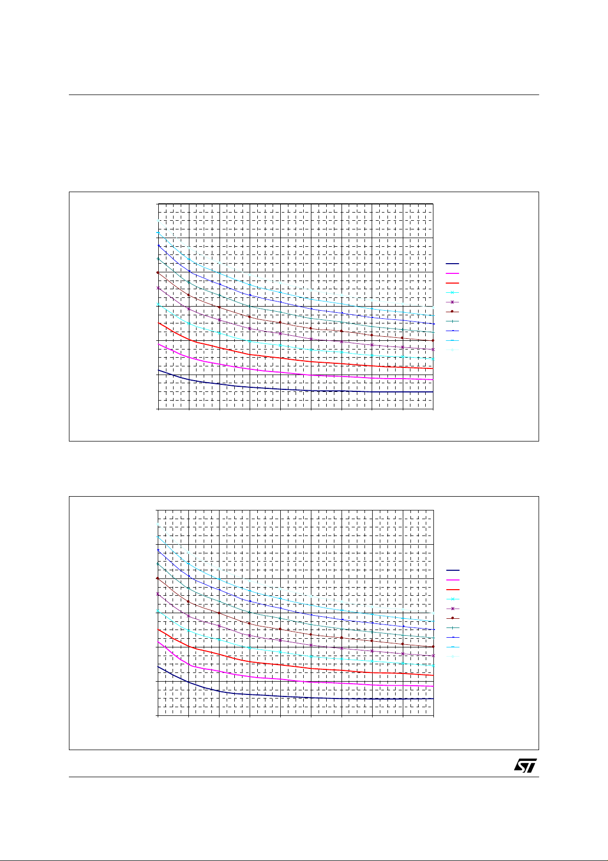
Figure 38 depicts the dependen cy of the efficiency on load applied to the 5V output (parameter is l oad
current on 15V output). Similarly, figure 39 shows the dependency on t he 15V output current (parameter
is load current on 5V output). Figures 40 a nd 41 s how the same characteristics as figures 38 and 39 but
measured at input voltage of 375 VDC.
Figure 38: Efficiency variation with 5V Output Current at 125VDC Input Voltage (Parameter is loaded
current on 15V output)
80
75
70
65
60
55
Efficiency [%]
50
45
40
35
20mA
40mA
60mA
80mA
100mA
120mA
140mA
160mA
180mA
200mA
30
61626364656
Output Cu rr ent [m A]
18/24
Page 19

Obsolete Product(s) - Obsolete Product(s) Obsolete Product(s) - Obsolete Product(s)
AN1934 - APPLICATION NOTE
Figure 39: Efficiency variation with 15V O utput Current at 125VDC Input Voltage (Parameter is loaded
current on 5V output)
80
75
70
65
60
55
Efficiency [%]
50
45
40
35
6mA
12mA
18mA
24mA
30mA
36mA
42mA
48mA
54mA
60mA
30
20 40 60 80 100 120 140 160 180 200
Output Cur rent [mA]
Figure 40: Efficiency variation with 5V Output Current at 375VDC Input Voltage (Parameter is loaded
current on 15V output)
65
60
55
50
45
Efficiency [%]
40
35
30
20mA
40mA
60mA
80mA
100mA
120mA
140mA
160mA
180mA
200mA
25
6 1626364656
Output Current [m A]
19/24
Page 20

Obsolete Product(s) - Obsolete Product(s) Obsolete Product(s) - Obsolete Product(s)
AN1934 - APPLICATION NOTE
Figure 41: Efficiency variation with 15V O utput Current at 375VDC Input Voltage (Parameter is loaded
current on 5V output)
65
60
55
50
45
Efficiency [%]
40
35
30
25
20 40 60 80 100 120 140 160 180 200
Output Current [mA]
50mA
100mA
150mA
200mA
250mA
300mA
350mA
400mA
450mA
500mA
The feedback loop stability and response to load transients are demonstrated from figures 42 to 45.
Figure 42: Load transient response, 20mA to
0.2A on 15V output, 5V output
unloaded, Vin= 127VDC
Figure 43: Load transie nt response, 20mA to
0.2A on 15V output, 5V output loaded
by 60mA, Vin= 127VDC
20/24
Page 21

Obsolete Product(s) - Obsolete Product(s) Obsolete Product(s) - Obsolete Product(s)
AN1934 - APPLICATION NOTE
Figure 44: Load transient response, 20mA to
0.2A on 15V output, 5V output
unloaded, Vin= 373VDC
Conducted emissions were measured in neutral and line wire using a peak or average detector. The
measurements were performed at 230VAC input voltage and both out puts were fully loa ded. Th e res ults
can be seen from figures 46 to 48.
Figure 46: Phase L, peak detector
Figure 45: Load transie nt response, 20mA to
0.2A on 15V output, 5V output loaded
by 60mA, Vin= 373VDC
21/24
Page 22

Obsolete Product(s) - Obsolete Product(s) Obsolete Product(s) - Obsolete Product(s)
AN1934 - APPLICATION NOTE
Figure 47: Phase N, average detector Fi gure 48: Phase N, peak detector
2.4 NON ISOLATED FLYBACK -5V/500mA, +10V/200mA (VARIANT 4)
2.4.1 Operating Conditions
Input Voltage range
Input Voltage Frequency range
Main Output (regulated)
Second Output
Total Maximum Out pu t Power
2.4.2 Circuit Operation
Variant 1 can be switched to variant 4 by removing short R16 and placement of R15. This reconfiguration
will make previous +5V output terminal from variant 1 as a common ground. Previous output ground from
variant 1 is disconnected from input ground and is referenced as -5V terminal. The total schematic of the
power supply can be seen in figure 49.
90-264 VAC
50/60 Hz
-5V / 500mA
10V / 200mA
5.5W
22/24
Page 23

Obsolete Product(s) - Obsolete Product(s) Obsolete Product(s) - Obsolete Product(s)
AN1934 - APPLICATION NOTE
Figure 49: Schematic Diagram of Non Isolated Flyback Converter (Variant 4)
90...264V ~
CON1
L
N
clamp
D4
EF16/4.7
AL = 120nH
Gap = 0.22mm
D1
GL1M
1000V
1A
D2
GL1M
1000V
1A
C1
22uF
400V
KMG
R1
10R
3W
L
1
2
N
Layout Hints: C5, C8 have
to be close to VIPer12A
Assembly options:
(4): -5V/500mA, +15V/200mA
note: all voltages refer to
neutral
L1
330uH 190mA
+
BC
C2
10uF
400V
KMG
C6
100pF
500V
+
R15
0R
100R
R17
0R
R3
8
2
T1A
3.1mH
160 turns
0.18 CuLL
VDD
Drain15Drain26Drain37Drain4
Sou rce11Sou rce2
VIPer12AS
15
56
4 3
U1
4
3
FB
C8
22nF
T1B
33uH
16.5 turns
0.315 CuLL
T1 C
10uH
9 turns
0.315 CuLL
C5
+
10uF
50V
KME
STPR120A
200V 1A
D5
STPS1L40A
40V 1A
D7
LL4148
R11
4.7k
BC856B
Q2
BC856B
C3
+
120uF
35V
LXY
R2
4.7k
Q1
TS2431ILT
R14
0R
C4
+
220uF
35V
LXY
+10V
R9
470R
R10
1k
C9
100nF
U2
-5V
C10
1nF
R8
4.7k
+10V
CO N2
3
2
1
cla mp
-5V
R5
4.7k
R7
4.7k
3. CONCLUSION
Several variants of the reference board based on a non isolated flyback conve rter built with monolithic
switcher VIPer12AS were presented. It was demonstrated, how the reference board can be easily
switched between variants or options. Depicted output regulation, waveforms, overall converter efficiency
characteristics and transient responses measured at different working conditions show good
performance of the reference boards. Also, thanks to the presented PCB layout and EMI input filter,
boards are EMI compliant with regards to the emissions as it was validated by presented EMI
measurements. All boards also passed EMI surge and burst tests for power supply immunity agai nst
incoming noise from mains.
23/24
Page 24

Obsolete Product(s) - Obsolete Product(s) Obsolete Product(s) - Obsolete Product(s)
AN1934 - APPLICATION NOTE
Information furnished is believed to be accurate and reliable. However, STMicroelectronics assumes no responsibility for the consequences
of use of such i nformat ion nor f or any infr ingement of patents or other rig hts of third par ties w hich may res ults from i ts use. No license is
granted by i m pl i cation or ot herwise under any patent or patent rights of STM i croelectr oni cs. Specifications mentioned i n this publication are
subject to change without notice. This publication supersedes and replaces all information previously supplied. STMicroelectronics products
are not authorized for use as critical compone nts in lif e support de vices or syste m s without ex press written approval of STMicroelectronics.
Austra lia - Brazil - Canada - Chin a - F i nl and - Franc e - Germany - Hong Kong - Ind i a - Israel - Italy - Japan - Malays i a -
Malta - Morocco - Singapore - Spain - Sweden - Switzerland - United Kingdom - U.S.A.
The ST logo is a trademark of STMicroelectronic s
2004 STMicroelectronics - Printed in ITALY- All Rights Reserved.
STMicroele ctronics GROUP OF C OM PANIES
http://www.st.com
24/24
 Loading...