

Page 1

AN1903
APPLICATION NOTE
A First Order Sigma Delta Converter Using ST52x440
1 INTRODUCTION
This application note shows the implementation of a Sigma-Delta (Σ∆) converter using a member of ST52
microcontroller family.
Although many devices of the ST52 family already have a built-in A/D Converter, another kind of converter
(precisely a Σ∆ converter) is implemented via sofware.
In this specific case, an ST52x440 is used. This device includes an Analog Comparator among its peripherals, which can also be used as a single slope ADC, thus allowing an easy implementation in firmware
of the SD conversion algorithm using few additional external elements.
The Σ∆ conversion algorithm is easily implemented in firmware using few additional external elements.
Attached you can find the firmware package.
2 SIGMA-DELTA THEORY
Sigma-Delta modulation has emerged as the architecture of choice for high-resolution analog-to-digital
conversion using simple and low-precision analog components. In this kind of converter an increased resolution is obtained reducing the conversion bandwidth or increasing the clock speed, over sampling the
signal to convert.
Over sampling has become popular because it avoids many difficulties encountered with conventional
methods for A/D and D/A conversion, especially in those applications requiring high-resolution and using
relative low-frequency signals. Moreover, sampling at high frequency eliminates the need for abrupt cutoffs in the analog anti-aliasing filters.
Classical Sigma-Delta circuits are composed of a Σ∆ Modulator, which provides a high-speed one-bit dat a
string followed by a digital filter and decimator to produce high-resolution data. The lowpass Σ∆ modulator
consists of one or more integrators and a one-bit quantizer. The basic con cept underlining Sigma-Delta
Converters is the use of feedback in order to improve the effective resolution of the quantizer.
Figure 1 shows a Σ∆ Converter block diagr am. The input signal is added t o the signal coming from the
feedback loop. This differentiated signal is then sent to the modulator. The comparator acts like a one-bit
quantizer, its output is sent to the D/A converter of the feedback branch and to a digital filter which provides
with time the multi-bit Digital Output.
1/8March 2004
Page 2
AN1903 - APPLICATION NOTE
Figure 1. Σ∆ Converter Block Diagram
Modulator
Modulator
Modulator
Modulator
Modulator
Modulator
Modulator
Differentiator
Analog
Analog
Analog
Analog
Signal
Signal
Signal
Signal
Input
Input
Input
Input
Differentiator
+
+
+_+_+
+
+_+_+
+_+_+
+_+_+_+
_
_
_
_
_
_
_
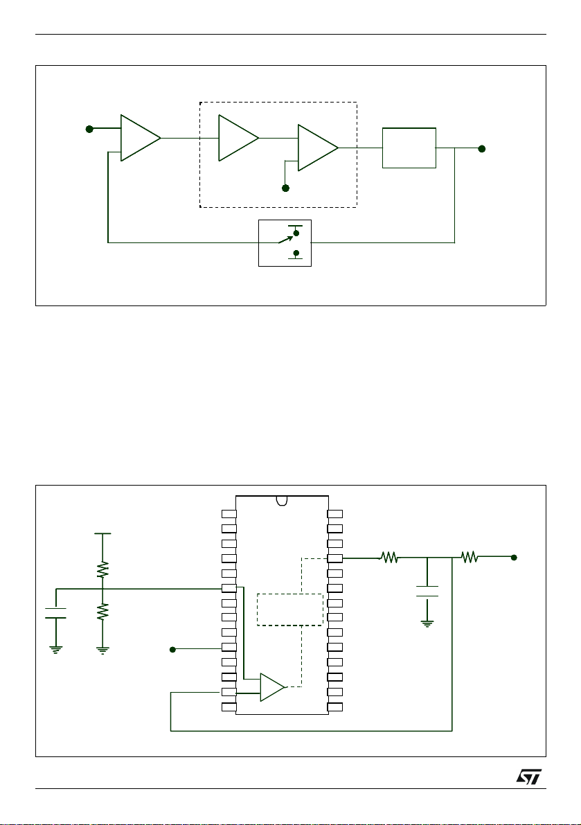
3 IMPLEMENTATION WITH ST52X440 MICROCONTROLLER
In Figure 2 a scheme of how the Σ∆ Converter is implemented with the ST52x440 microcontroller is shown.
If compared to a classical Sigma-Delta Converter, the external capacitor C
tor; the comparator is built inside; voltage reference V
means of two equal resistances R
mented by the firmware. By means of the two equal resistances R
conversion of signals in the range 0 divided by 5V is allowed.
When pin PC0 is set high by the feedback loop, the voltage at pin PB0 increases in magnitude until it becomes higher than V
consequently until the comparator sets PC0 high. In the meantime, the number of zeros occurring at the
. Once this has occurred, pin PC0 is set low and the voltage at pin PB0 decreases
REF
output of the comparator (which means integrated signal higher than reference signal) are count ed. This
number is strictly related to the input voltage V
Figure 2. Schematic
Integrator Comparator
Integrator Comparator
Integrator Comparator
Integrator Comparator
Integrator Comparator
Integrator Comparator
Integrator Comparator
+
+
+_+
+
+_+
+_+
∫
∫
∫
∫
∫
∫
∫
1- Bit D/A Converter
1- Bit D/A Converter
1- Bit D/A Converter
1- Bit D/A Converter
1- Bit D/A Converter
1- Bit D/A Converter
1- Bit D/A Converter
and R4; while the one-bit D/A Converter and the digital filter are imple-
3
+_+
_
_
_
_
_
_
_
V
V
V
V
V
V
V
REF
REF
REF
REF
REF
REF
REF
is supplied by partitioning the voltage VSS by
REF
3
.
IN
SW
SW
CORE
CORE
CORE
CORE
CORE
routine
routine
absolves the role of integra-
INT
Digita l
Digita l
Digita l
Digita l
Output
Output
Output
Output
and R4 (center scale set to 2.5V) to a
2/8
Vdd
OSCOUT
OSCOUT
V
V
dd
dd
R
R
3
3
R
R
4
4
Serial
Serial
OUTPUT
OUTPUT
OSCOUT
OSCIN
OSCIN
OSCIN
Vpp
Vpp
Vpp
PC4
PC4
PC4
PC3
PC3
PC3
PB7/CS
PB7/CS
PB7/CS
PB6/BG
PB6/BG
PB6/BG
PB5/AC5
PB5/AC5
PB5/AC5
PB4/AC4
PB4/AC4
PB4/AC4
PB3/AC3
PB3/AC3
PB3/AC3
PB2/AC2
PB2/AC2
PB2/AC2
PB1AC1
PB1AC1
PB1AC1
PB0/AC0
PB0/AC0
PB0/AC0
GNDA
GNDA
GNDA
ST52x440
ST52x440
V
V
REF
REF
Firmware
Firmware
closes loop
closes loop
_
_
+
+
Vdd
Vdd
Vss
Vss
Vss
RESET
RESET
RESET
R
R
1
PC0
PC0
PC0
PC1
PC1
PC1
PC2
PC2
PC2
PA7/INT/ACSYNC
PA7/INT/ACSYNC
PA7/INT/ACSYNC
PA6/TRES/TOUT
PA6/TRES/TOUT
PA6/TRES/TOUT
PA5/TCLK
PA5/TCLK
PA5/TCLK
PA4/TSTRT
PA4/TSTRT
PA4/TSTRT
PA3/ACSTRT
PA3/ACSTRT
PA3/ACSTRT
PA2/MAIN2/TOUTN
PA2/MAIN2/TOUTN
PA2/MAIN2/TOUTN
PA1/MAIN1
PA1/MAIN1
PA1/MAIN1
PA0/TROUT
PA0/TROUT
PA0/TROUT
1
R
R
2
2
V
V
IN
IN
C
C
INT
INT
Page 3
AN1903 - APPLICATION NOTE
When the signal to be converted comes from a high impedance source, a buffer has to be placed between
this signal source and the input terminal of R2 in order to decouple impedances.
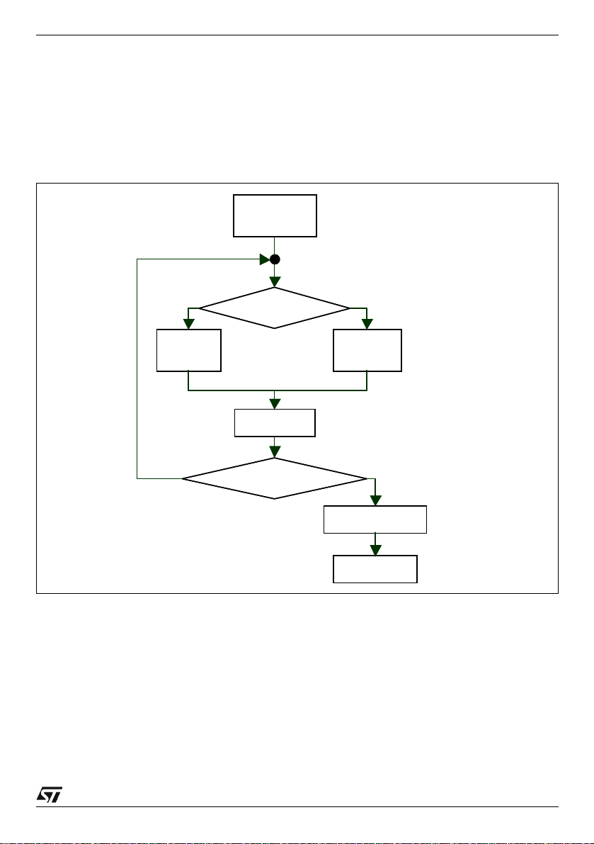
In Figure 3 a flow chart of the firmware used is shown. When V
is higher than the reference signal pin PC0 is set low and the variable result is incremented; otherwise
PC0 is set high and padding instructions are executed in order to keep all paths t hrough t he c ode equal.
As soon as the variable Counter reaches value 2
result obtained is filtered and then serially shown through pin PB3. Serial communication is implemented
by software by means of the internal timer, which fixes the BAUD rate.
Figure 3. Fl o w C hart
N
-1 (with N = num of bits) the result is stopped and the
Result = 0
Result = 0
Counter = 0
Counter = 0
V
> V
V
> V
PB0
ref
PB0
ref
?
?
(which is the input to the comparator)
PB0
YESNO
YESNO
PC0=1
PC0=1
Padding
Padding
Counter ++
Counter ++
Counter= 1023?
Counter= 1023?
4 FIRMWARE
The implementation used in this application performs the comparison between the integrated signal and
the reference signal, the calculation of the result and closes the feedback loop. Moreover, it processes the
results and gives them serially to the output pin PB3 so that they can be acquired, displayed and eventually processed by a PC.
The software was developed in Visual FIVE, the visual Development Tool of the ST FIVE Family of micros
and it is displayed in the following section.
Figure 4 and 5 are two screens taken from the attached firmware developed in VisualFIVE describing respectively the flow chart of the main program and the result computation algorithm.
PC0=0
PC0=0
Resul ++
Resul ++
YESNO
YESNO
10 bits Æ 8 bits
10 bits Æ 8 bits
Show Value
Show Value
3/8
Page 4

AN1903 - APPLICATION NOTE
Figure 4. Main Loop
4/8
Page 5

Figure 5. Result Computation
AN1903 - APPLICATION NOTE
The following steps refer to the attached firmware too.
4.1 Peripheral Con figuration and Micro Ini tialization
In this step, the micro is initialized, in particular with:
– timer: it is configured to work @ 1.25 MHz, interrupt source on rising edge, Timer Count = 131(in order
to have BAUD rate equal to 9600 bits/s);
– triac driver: configured to work in PWM mod e;
– A /D : set in comparator mode;
– watchdog: counting period equal to 15.6 ms
– initialization of the ports (analog input, digital input/output).
5/8
Page 6

AN1903 - APPLICATION NOTE
4.2 Result Computation and Loop Closing
Each cycle consists of two phases: during the first c yle, data is acquired , while during th e second cy cle,
data is shown.
While converted data is processed and shown, the capacitor C
age and on the last comparator output. In order to keep initial conditions independent from the input voltage for each conversion, data is acquired as soon as transition (0/1) is detected at the output of the
comparator. This is achieved by using two variables. One is used to store the old value of the comparator
output and the other one stores the current value. As soon as these two variables become different, computation starts. Comparator output is sent to pin PC0 closing the feedback loop. If this value is high the
variable result is incremented; otherwise padding instructions are executed.
4.3 Result Shown
The digits of the result are changed into ASCII and are serially sent to pin PB3. The timer synchronizes
the transmission permitting a serial communication at 9600 baud. Sampling frequency is set by triac driver
peripheral used as a timer; in fact it generates an interrupt each 15.6 ms and the conversion starts as soon
as this interrupt occurs.
Output data can be acquired by Windows HyperTerminal.
5 CONCLUSION
Some results are shown here.
Two different signals were used as input signals: a saw tooth waveform and a triangular wave form both
signals have a 100mHz frequency and a 0
ures 6 and 7 the respective output signals are plotted.
Figure 6. Sawtooth Waveform - Output
÷ 5 V range (thus with an output signal in 0\255 range). In Fig-
is charged depending on the input volt-
INT
6/8
250
200
150
8bit-Result
100
50
0
200 300 400 500 600 700 800 900
Samples
Page 7

AN1903 - APPLICATION NOTE
Figure 7. Triangular Wave Form - Output
250
200
150
8bit-Result
100
50
0
500
600 700 800 900 1000 1100
Samples
6 REFERENCES
1. S.R. Norsworthy, R. Shreier, G.C. Temes “Delta-Sigma Data Converters, Theory, Design and Simula
tion”, New York - IEEE PRESS, 1996
2. J.C. Candy, G.C. Temes “Oversampling Delta-Sigma Converters”, New York - IEEE PR ESS , 1991
7/8
Page 8

AN1903 - APPLICATION NOTE
Information furnished is believed to be accurate and reliable. However, STMicroelectronics assumes no responsibility for the consequences
of use of such information nor for any infringe ment of patents or other right s of third p arties which may re sult from its use. No license is granted
by implication or otherwise u nder any pat ent or pate nt righ ts of S TMicr oelect ronics. S pecif ica tion me nti one d in this pu blic ation are subject to
change without notice. This publication supersedes and replaces all information previously supplied. STMicroelectronics products are not
authorized for use as critical components in life support devices or systems without express written approval of STMicroelectronics.
Australia - Brazil - China - Canada - Finland - France - Germany - Hong Kong - India - Israel - Italy - Japan - Malaysia - Malta
The ST logo is a registered trademark of STMicroelectronics
© 2004 STMicroelectronics – Printed in Italy – All Rights Reserved
STMicroelectronics GROUP OF COMPANIES
- Morocco - Singapore - Spain - Sweden - Switzerland - United Kingdom - U.S.A.
http://www.st.com
8/8
 Loading...