


AN1902
Obsolete Product(s) - Obsolete Product(s) Obsolete Product(s) - Obsolete Product(s)
®
- APPLICATION NOTE
VIPower: HF CO NVERTER BASED ON VK 06TL
DEVICES TO DRIVE 58W TL TUBES
N. AIELLO - S. MESSINA
This document des cribes a re ference desi gn for Lightin g Ballast dedicate d to drive 58 W T8 tubes. The
board accepts DC in put vo l tage (u p to 430V ) reali zing the c athod es pr ehea ti ng, t he E oL prot ecti on a nd
the maximum current limitation. It is based on the new VK06 device that integrates the controller and the
Power stage on the same chip. It is housed in SO-16 and SIP-9 packages.
INTRODUCTION
The European Comm unity has agreed on a new direct ive for banning electro magnetic control gea r for
fluorescent lamps. The aim is to improve the system efficiency (EEI-Energy Efficiency Index) reducing
the environmen tal impact. This new di recti ve div ide s the b all ast in different classe s fr om A1 to D . A1 is
the most efficient system, D the least efficient.
■ A1 → Dimmable electronic
■ A2 → Low-loss electronic
■ A3 → Standard electronic
■ B1 → Extra low-loss magnetic
■ B2 → Low-loss magnetic
■ C → Normal-loss magnetic
■ D → High-loss magnetic
Since 1998, the energy classi fication has be come compulsory and it has be en inserted in a Cenelec
standard. It means:
- since April 2002, all ballasts with an EEI of D are banned;
- starting from October 2005, all ballasts with an EEI of C will be banned.
Thus the market is aski ng for cost effectivene ss, good per formance, l ow noise and com pact ballasts to
feed this kind of applications. The VK06 is a very suitable device, satisfying all the requirements with few
external components.
The proposed reference design can supply 58W T8 FL tube with preheating function and EoL
protection. Being the design reference focused on the converter realization (we don ’t co ver the PFC
stage) it has been set to give out the right output power when 400V dc voltage is applied.
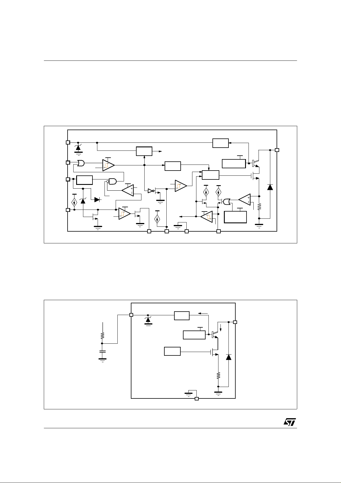
1. VK06 DESCRIPTION
The VK06 is a monolithic device made by using the VIPower® M3-3 STMicroelectronics proprietary
technology that integrates in the same chip a vertical flow Power stage and a BCD based control circuit.
The Power stage is made by a high v oltage Bipolar transistor together with a low voltage n-channel
MOS transistor in emitter switching configuration Its performances are a good trade-off betwee n the
Bipolar transisto r low drop/hig h breakdow n voltages and the MOS transi stor hi gh switching s peed. The
block diagram is shown in figure 1.
March 20 04 1/32
Obsolete Product(s) - Obsolete Product(s) Obsolete Product(s) - Obsolete Product(s)
AN1902 - APPLICATION NOTE
In the control part the following sections can be analyzed:
1) Supply
2) Oscillator/Trigg er
3) Diac
4) Protections
Figur e 1: VK06 Internal Block diagram
VCC
SEC
DIAC
CapPREH
Vdd
CLAMP
Vref1
DIAC
Reset
Preheating
Vcc
diac on/off
COLL
sec on/off
protection
Vref3
Vcc
Vcc
Reset
CAP1
Vdd
Vref2
Vdd
Supply
Vref4
CAP2 CAP1 GND
Delay on
protection
Gate Driver
latch
Vcc
Vcc charge
VddVcc
Vref6
CapEOL
Bipolar Driver
Over Curr ent
Detector
Over Temperature
Detector
Vcc
Vcc
Vref5
COLL
sense
R
1.1 SUPPLY (Figure 2)
The device is supplied from the VCC pin connected to an R-C network. From VCC both the control and the
power stage are supplied. A t start up the supply capacitor is charged through a resistor and only few
hundreds µ A are ne eded. Duri ng the opera ti on the devic e is s elf-supplied recovering o n VCC the charge
taken from the Power Bipolar base at turn-off. The voltage on VCC is internally clamped at ~6.8V.
Figur e 2: Internal Supply Block
Bipolar Driver
Ic
Vcc
R
COLL
Ic
sense
DC BUS
VCC
CLAMP
Vcc charge
Gate Driver
GND
2/32
Obsolete Product(s) - Obsolete Product(s) Obsolete Product(s) - Obsolete Product(s)
AN1902 - APPLICATION NOTE
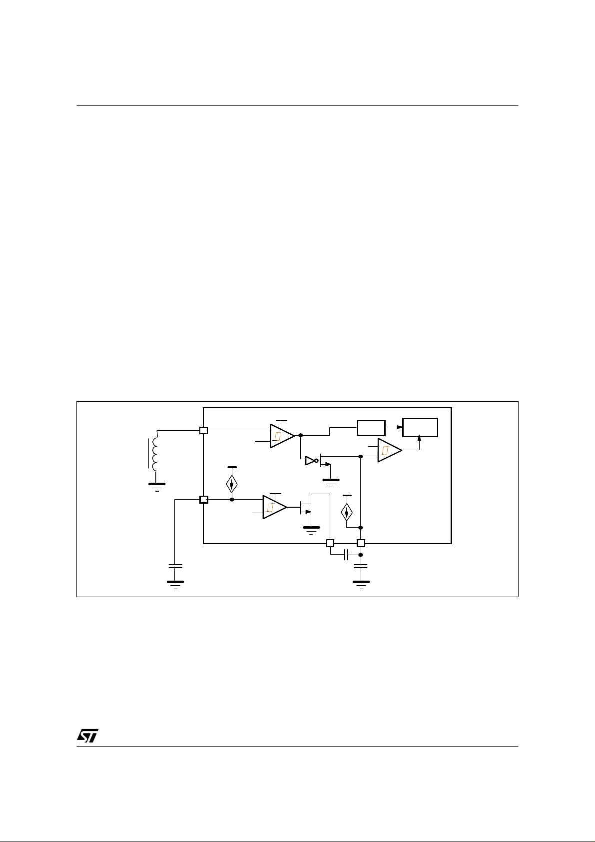
1.2 OSCILLATOR/TRIGGER (Figure 3)
It fixes the conver ter working frequenci es (preheating, ign ition, and steady-state ). The tON (conducti on
time) is set using S EC, CAP1, CAP2 and C apPREH pins. T he device is tri ggered ON when the voltage
on SEC reache s ~2.2V. When this condition is detected the Pow er stage is switched ON and internal
current gene rators start to give co nstant currents to C AP1 and CapPREH. T he device will be switched
OFF when one of the two following conditions is present: the voltage across CAP1 is equal to the internal
voltage referenc e (~2.3V), the voltage on S EC is lower than 0.9V. Using a capacitor on CapPREH and
the two frequency capacitors on CAP1 and CAP2 it is possible to have both preheating and steady state
frequencies. Until the voltage on CapPR EH is lower than 4.2V only the Cfpreh (capaci tor connected to
CAP1) will be cha rged setting the prehea ting frequency. When 4.2V on CapPRE H pin is overcome, an
internal switch puts in parallel Cfpreh with the Cfst capacitors (connected between CAP1 and CA P2)
lowering th e fre quency to the steady-state one. The value of CapPREH fixes t he pr ehea ting dur ati on. In
all the operative conditions the frequency capacitors will be discharged when the voltage on SEC
becomes lower than 0.9V.
During the la mp igni tion the frequency cont rol is realized throug h the secondary wi ndin gs wou nd o n the
primary choke and connected to the SEC pins. In this phase the voltage on SEC reaches 0.9V before the
tON is set by the f requency capacitors. The system oscillate at its resonance freq uency (higher than
steady state one ) allowing the tube igniti on. After the tube ignition the tON will be set by the frequenc y
capacitors.
An internal delay at Power turn-on avoids the hard switching condition.
Figur e 3: Internal oscillator/trigger block
Vcc
Vcc
Reset
CAP1
CAP2 CAP1
Cfst
Vdd
2.3V
Delay o n
Cfpreh
Gate Driver
SEC
2.2V
Vdd
CapPREH
4.2V
Cappreh
1.3 DIAC (Figure 4)
Through the DIAC pin two functions are achieved: start of oscillations and reset of the preheating
capacitor CapPREH.
1) St art of oscillation: in OFF condition (voltage on the SEC pin lower than 2.2V) the device can be turned
ON when t he voltage across DIAC ov erco mes ~ 28V. An HV diode keeps the DIAC low when the Po wer
stage is ON.
2) Reset of preheating capacitor: in order to guarantee the right preheating timing the preheating
capacitor must be discharg ed before starti ng oscilla tions. To realize this function a switch on CapPREH
3/32
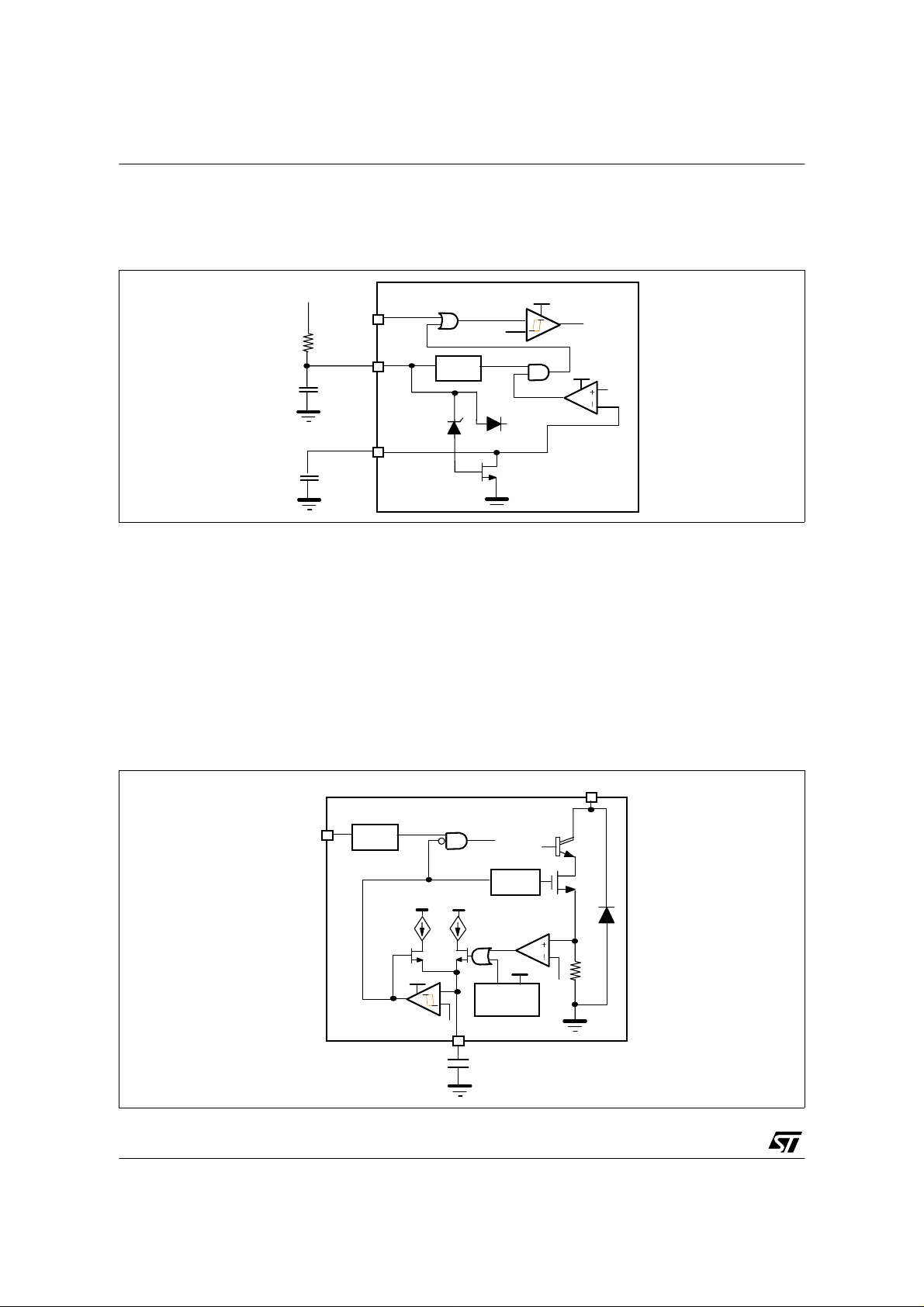
Obsolete Product(s) - Obsolete Product(s) Obsolete Product(s) - Obsolete Product(s)
AN1902 - APPLICATION NOTE
pin is activated when the voltage across DIAC pin overcomes ~12V. On the other side the diac can
activate the circuit only when the voltage on CapPREH becomes lower than ~0.6V.
Figur e 4: Internal diac block
DC BUS
DIAC
CapPREH
Cappreh
SEC
DIAC
Reset
Preheating
Vref1
diac on/off
COLL
Vcc
sec on/of f
Vcc
0.6V
1.4 PROTECTIONS (see figure 5)
The device is protected against over-current and over-temperature. Both protections are activated
connecting on the CapEOL p in a capacitor that fixes the timing. T he over-curren t protection works as
follows: an internal Rsense checks the cur rent through the Power stage and if it exceeds ~1.5A, an
internal generator gives current to CapEOL pin. When the voltage across CapEOL pin reaches ~4.3V the
Power stage is kep t OFF, the diac is deactivated and the current consum ption from VCC is lowered. At
the same time another current generator is activated latching the device in OFF state.
The thermal prote ction is activated when the junction temperatu re exceeds ~150°C. This block, wh en
activated, acts on the same EoL circuit latching the device.
Figur e 5:. Internal protections block
COLL
Vcc
Vcc
Capeol
diac on/off
Vdd
4.3V
Gate Driver
Over Current
Detector
Vcc
Over Temperature
Detector
CapEOL
Rsense
Vref
DIAC
DIAC
latch
protection
4/32
Obsolete Product(s) - Obsolete Product(s) Obsolete Product(s) - Obsolete Product(s)
AN1902 - APPLICATION NOTE
2. PACKAGES
The VK06 is ass embled in two different packages in order to cover both the s urface mounting and the
through-hole PCB. The packages are the SO-16 narrow and the SIP-9 (see figure 6).
Figur e 6: Package outline and pin configuration
9
16
8
1
1
9
SO16 PACKAGE SIP9 PACKAGE
N° pin Name N° pin Name
1 CAP1 1 CAP1
2 CapPREH 2 CapPREH
3 GND 3 GND
4DIAC 4DIAC
5 SEC 5 COLL.
6V
CC
7CAP2 7V
6SEC
CC
8 CapEOL 8 CAP2
9÷16 COLL 9 CapEOL
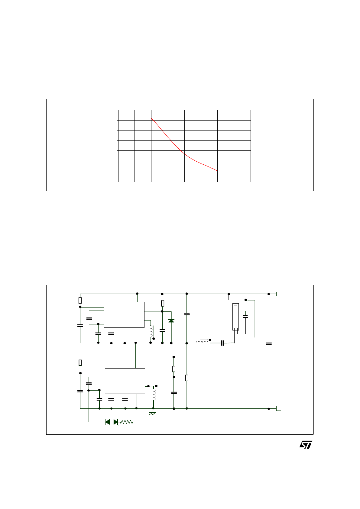
In figure 7 the SO-16 thermal characterization is reported. In this package eight pins are connected to the
tab to reduce the junction-pin thermal resistance whereas the case-ambient thermal resistance is related
to the copper a rea on the P CB (device h eat-s ink). The devi ce has bee n charac terized at th ree differe nt
copper ar eas: 0.5, 1 and 2 cm2; at three different po wer dissipatio ns: 0.25, 0.5 and 1W an d measur ing
the devices case temperatures.
Figur e 7: SO-16 R
th case-ambient
°C/W
Vs. PCB Copper Area
160
150
140
130
120
110
100
90
80
70
60
50
0 0.5 1 1.5 2
Rth case-ambient
1W 0.5W 0.25W
Cm
2
5/32
Obsolete Product(s) - Obsolete Product(s) Obsolete Product(s) - Obsolete Product(s)
AN1902 - APPLICATION NOTE
In Figure 8 the SIP-9 thermal characterization (no heat-sink) is reported.
Figur e 8: SIP-9 R
th case-ambient
[°C/W]
(no heat-sink)
46
45
44
43
42
41
40
39
0 0.25 0.5 0.75 1 1.25 1.5 1.75 2
Rth case-ambient
[W]
3. CONVERTER DESCRIPTION
In figure 9 th e elec t ric al sc hem e, re ali zing a v oltage-fe ed c on verte r based on VK06 is repo rted. The two
windings Ls connected to the S EC p ins are wou nd on th e chok e Lp. Four different o perative phases can
be described:
- start-up
- preheat
- steady state
- ignition
Figur e 9: Typical application circuit
R14
C12
R1
C3
C15
C16
C10
C6
VCC
CAP2
CAP1
CapPREH
VCC
CAP2
CAP1
CapPREH
C9
CapEOL
CapEOL
COLL
DIAC
SEC
GND
Ls
COLL
DIAC
SEC
GND
C8 C7
Ls
R15
C11
Dz2
R3
C4
C14
R10
Lp
Tube
C2
DC BUS
C1
Cbulk
D1 Dz1 R6
6/32
Obsolete Product(s) - Obsolete Product(s) Obsolete Product(s) - Obsolete Product(s)
AN1902 - APPLICATION NOTE
3.1 START-UP
As soon as the system is supplied, the VCC capacitors C3 and C1 2 start to be ch arged from the DC bus
respectively by means of the resistors R1 and R14-R10. At the same time, the low side diac capacitor C4
starts to be charged by the resistor R3. The network R15-C11 biases the high side DIAC.
In normal ope rations the l ow side device is the one to go o n the fir st time, wh ile in the h igh side d evice
the DIAC pin, clamped by Dz2, is used only to reset the preheating capacitor C9.
As soon as the voltage on C4 reaches about 28.5V the diac block switch ON the device. At that time both
devices must b e biased with the minim um requested VCC voltage (~ 5V) in order to make the system
oscillate properly.
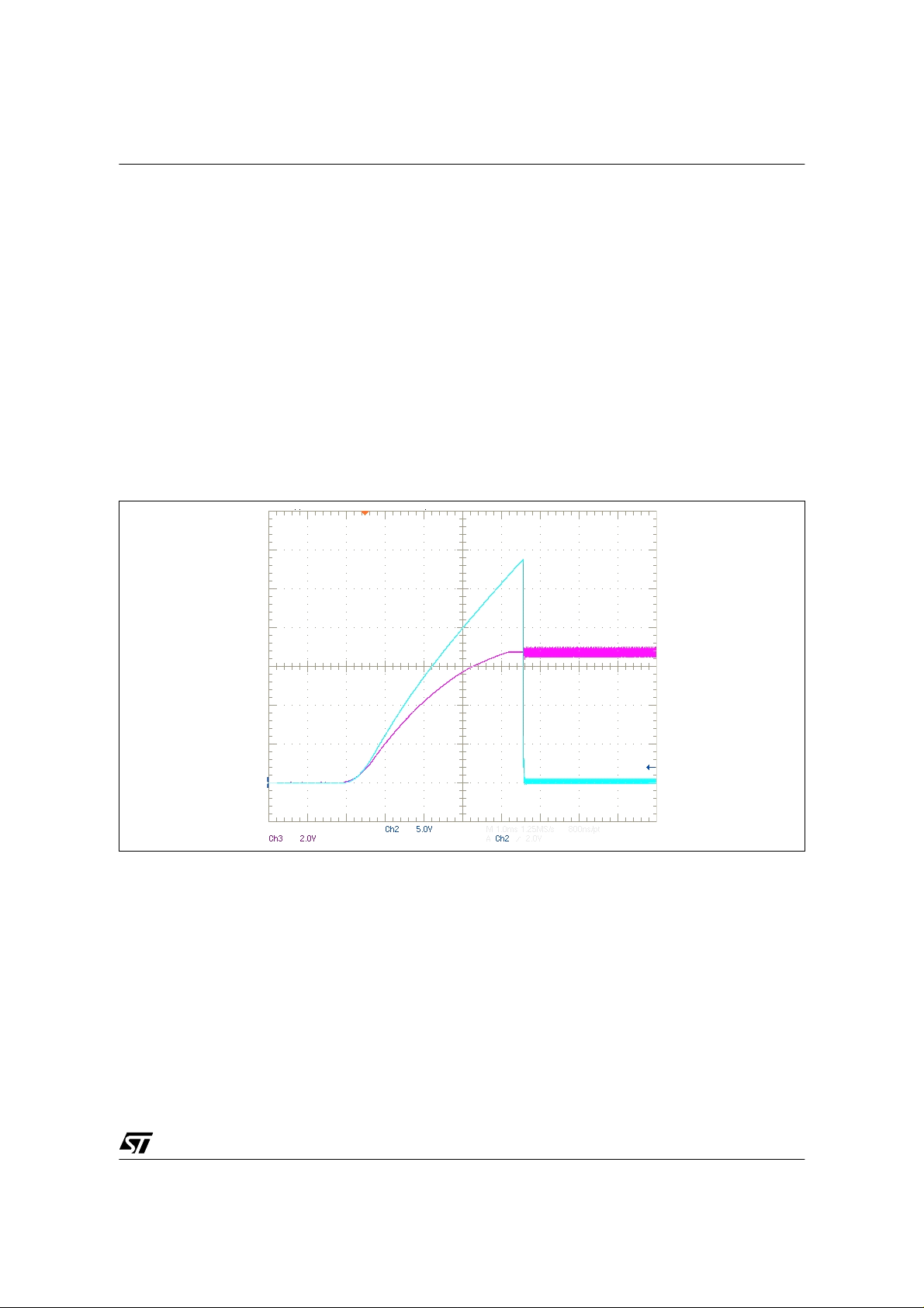
In figure 10 low side (LS) diac and VCC typical wave forms are shown. In the picture the VCC voltage
reaches 6.8V after 4.2 m sec rema ini ng constant at th is value (it is internally clampe d) until the converter
starts to oscillate. At that time the storage charge recovery will be responsible f or the device supply,
charging the VCC capacitor at the final voltage value (~6.8V).
Figure 10: Typical start-up operation
LS DIAC pin voltage
For the diac and VCC biasing networks the following choices can be done:
R14=R10; R14+R10=R1; C3=C
R15>>R
With this setting the converter midpoint will stay at V
the same for any DC bus voltage.
For a proper start up phase the following condition has to be satisfied:
14
dcbus/2
LS V
pin voltage
CC
12
and the voltages across C3 and C12 will be
VC3=V
≥ 5V when V
C12
=28.5V
C4
7/32
Obsolete Product(s) - Obsolete Product(s) Obsolete Product(s) - Obsolete Product(s)
AN1902 - APPLICATION NOTE
Where:
τ
Vc3=R1
The networ k R15-C11 must be chosen to have the co mplete discha rge of C9 when th e low side diac
strikes the converter. The zener diode Dz2 (~18V) clamps the DIAC pin below the diac activation
threshold.
During oscillations the diac capacitors C4 and C11 will be discharged b y the in ternal diod es connect ed
between DIAC and Power collector while the VCC capacitor will be charged by the charge recovered from
the Power stage (see figure 11).
Figur e 11: Typical waveforms after the diac strike
Mid point voltage
• C
τ
Vc4=R3
3
= (R
• C
14 + R10
(low side)
4
) • C
12
LS VCC pin voltage
LS DIAC pin voltage
3.2 PRE-HEAT
Still referring to the figure 9, the capacitors C7-C9 (with C7=C9) fix the cathodes preheating time
duration. The preheating frequency is set by the capacitors C10-C6 (with C10=C6).
3.2.1 PRE-HEATING TIME
CapPREH pin supplies a constant current I
capPREH
~
55µA. This current is supplied only during the t
ON
.
The preheating ends when 4.2V is reached on CapPREH.
Assu ming that
V
∆ 4.2V=
CapPREH
I
CapPREH
the preheating time t
55µA≅
will be:
preh
V
∆
CapPREH
t
preh
-------------------------- -
C7
• 0.15s==
I
CapPREH
---------------------
2
/µF
8/32

Obsolete Product(s) - Obsolete Product(s) Obsolete Product(s) - Obsolete Product(s)
AN1902 - APPLICATION NOTE
3.2.2 PRE-HEATING FREQUENCY
For the pre-heating frequency calculation the following considerations can be done:
1
--
f
=
1
-- -T t
2
ON
++=
t
storage
t
dVdt
T
t
storage
const 300n≈= sec
(storage duration of the device Power stage)
tdV/dt is the duration of the snubber capacitor (C14) charge during the half-bridge mid-point commutation
between ground and VDC bus.
It can be calculated using the following relationship:
t
dV/dt
= C
snubber
x
∆V/i
peak
where:
■ ∆V (DC bus voltage);
■ i
(peak current);
peak
■ C
(snubber capacitance).
snubber
tON is the conduction time fixed by the preheating frequency capacitor (C6) and device characteristics.
It can be calculated according to the following formula:
tON=K • C6
Where K=6.7µsec/nF (fixed by the VK06)
3.3 STEADY STATE
The steady stat e fre quen cy is se t by the par all el of the capac itors C 6- C16 for the l ow si de a nd C10- C 15
for the high side, where C16=C15. The same formulae of the preheat can be applied:
1
--
f
=
1
-- -T t
2
t
storage
ON
++=
const 300n≈=
t
storage
t
dVdt
sec
t
ON
KC6C16+()=
T
3.4 IGNITION
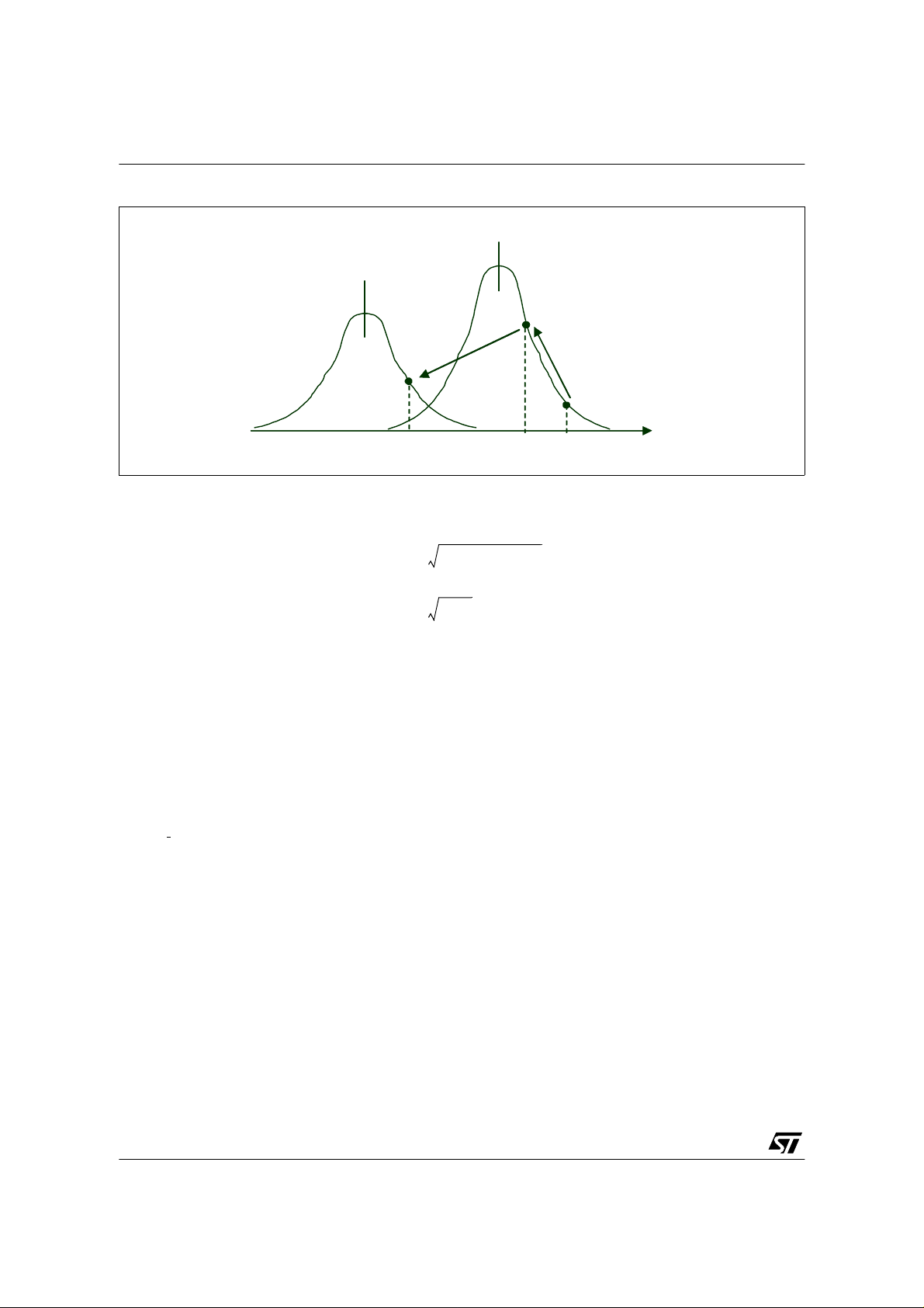
The converter of figur e 9 has two different resonan ce frequencies, the firs t one before the tube igni tion
the second o ne after the tube ignition . Th e con verte r operation from preh eat to st e ady state is shown in
figure 12.
9/32
Obsolete Product(s) - Obsolete Product(s) Obsolete Product(s) - Obsolete Product(s)
AN1902 - APPLICATION NOTE
Figure 12: Load typical resonance curves
Resonance frequency
after the tube ignition (f2).
Where the two frequencies are:
f
1
f
2
3
------------------------------------------------
=
2
π L
-----------------------
=
2
π L
1
seriesC
()
PC1
1
PC2
Resonance frequency
before the tub e ignition(f1).
2
1
fpreh
fign fsteady
(before the tube ignition)
2
(after the tube ignition)
f
In good b allast design the cathode prehe ating is requeste d in order to increase the tub e lifetime. I t is
obtained making high curren t flow through the cathodes for a fixed time. A simple rule for the prehea ting
efficiency check is reported:
1) measure the cathode resistance at the beginning of the preheating;
2) measure this resistance at the end of the preheating;
3) if its value is increased 3-4 times, the cathodes will work at the right temperature during ignition.
During the preheating the current level has to be able to heat the cathodes without generating the ignition
voltage on the start-up capacitor C1. Still referring to figure 12, the converter will operate as follows: it will
start working at the pre heat in g frequ ency (do t 1) that mu st be higher than the re sonance freque nc y f1. It
will remain in this condition for the time fixe d by the preheating capacitor. After the preheating the device
frequency control is taken by the two secondar y windings mov ing the working fre quency up to the dot 2
where the tube is supposed to ignite. Once the tube is ignited the converter resonance frequency is
lowered to f2 and the conver ter can work at the steady state frequency (dot 3) fixed by the o scillato r
capacitors.
In figure 13 the complete start-up sequence is shown.
10/32

Obsolete Product(s) - Obsolete Product(s) Obsolete Product(s) - Obsolete Product(s)
Figure 13: T ypical converter operation from start-up to steady state
AN1902 - APPLICATION NOTE
Preheating
Ignition
3.5. PROTECTIONS
The converter is protected against:
- End of Life (EoL)
- Overtemperature
- Overcurrent
3.5.1 End of Life
If the tube is in EoL conditi on it w ill not ignite any mo re for cing the c onve rter to work at its reson ance (f1 )
with very high current levels. This condition must be checked, stopping the oscillation, before the system
destruction for high power dissipation. In the suggested converter (figure 9) the EoL condition is detected
in the low side VK06 using the capacitor C 8 connected to C apEOL pin. Th is pin is shorted (di sabled) i n
the high side device.
The protection is activated as follows: an internal Rsense checks the current through the Power stage. If
this current exceeds ~1.5A an internal generator supplies current (i
soon as the voltage acros s CapEOL p in reaches ~4.3V (∆v
diac is deacti vated and the curr ent consu mption from VCC is lowered. At the same time another c urrent
generator is activated latching the device. This condition is maintained until the DC bus voltage is
present. Th e duration of EoL co ndition before latch ing is establishe d by C8 according to the f ollowing
considera tions.
I
t
×
EOL
C
8
M
---------------------
=
∆
v
EOL
Steady-state
about 350µA) to CapEOL pin. As
EOL
) the Pow er stage is switched OFF, the
EOL
11/32

Obsolete Product(s) - Obsolete Product(s) Obsolete Product(s) - Obsolete Product(s)
AN1902 - APPLICATION NOTE
where:
IM = average current flowing into C8 during the period of oscillation. Referring to the figure 14, IM can be
i
×
EOLtch earg
-------------------------------
I
M
f is the frequency during EoL condition (~ resonance frequency)
Combining the equations we obtain:
C
Figure 14: Device current during the EoL condition
T
i
× f t
EOLtch earg
--------------------------------------------------------
=
8
∆
× f×==
i
EOLtch earg
v
EOL
××
EOL
1.5A
t
Figure 15 sh ows the operation during the EoL condition. The ca pacitor C8 is maintained d ischarged
during the preheating phase and the oscillation are stopped as soon as it is charged to 4.3V
LS Collector current
charge
12/32

Obsolete Product(s) - Obsolete Product(s) Obsolete Product(s) - Obsolete Product(s)
Figure 15: Operation during the EoL phase
AN1902 - APPLICATION NOTE
Choke Curre nt
LS CapEOL pin Voltage
3.5.2 OVERTEMPERATURE
A thermal protection is activated when the junction temperature exceeds ~150°C. Its effect i s the same of
the EoL detection. For the timing definitio n it must be considered t hat the current gener ator on CapEOL
pin is activated during the tON of the device.
The duration of the over-temperature condition before latching (tTH) can be calculated as follows
v
∆
EOL
t
th
where:
i
= 350µA;
EOL
∆v
=4.3V.
EOL
3.5.3 OVERCURRENT
The network D1, Dz1 and R6 connected between SEC and CAP1 pins realizes the overcurrent
protection l imiting the maximu m accepted peak curr ent. This function is v ery useful during the ign ition
and the EoL, where the converter, working v ery close t o the resonanc e frequen cy (f1), can re ach very
high current levels (possibility of saturation of the transformer). This circuit is applied only on the low side
VK06. It works anticipating the device switch OFF when a defined current level is reached, in other words
the working frequency is incre ased. The modality is the following: an increasing in the current value
causes an i ncrease of t he seconda ry wind ing voltage (we are work ing at the reso nance frequen cy). As
soon as this voltage exceeds the zener Dz1 + diode D1 brea kdown, an amount o f current will flow into
-------------- -
C
×=
8
I
EOL
----------
2
13/32

Obsolete Product(s) - Obsolete Product(s) Obsolete Product(s) - Obsolete Product(s)
AN1902 - APPLICATION NOTE
the frequency capacitor anticipating the device switch-OFF. The resistance R6 limits injected current
realizing a d elay in the capacitor ch arge. The diode D1 d ecoup les SEC and CAP1 pins d uring t he OFF
state (negativ e voltage on SEC pin). In figu re 15 the EoL inte rventio n with th e current limited at 2,4A i s
shown.
3.6 MORE ABOUT THE TRIGGER
With high resist ive tubes the voltage on the secondary w indings could decrease very rapidly, reaching
the SEC pin switch-OFF threshold (0.9V), before than the internal oscillator switch OFF the device. This
cause an increase of the working frequency.
The phenome non can be explained as foll ows: the voltage drop on the chok e Lp is equal to V
minus the drop on the impedance made by the tube and C1 that is proportional to the current.
The voltage on the secondary windings is a fixed portion of the primary one. If the voltage on Lp becomes
zero no voltage will be transferred on SEC pin and the device will be switched-OFF.
The higher is the tube impedance the lower is the current level at which the situation can occur.
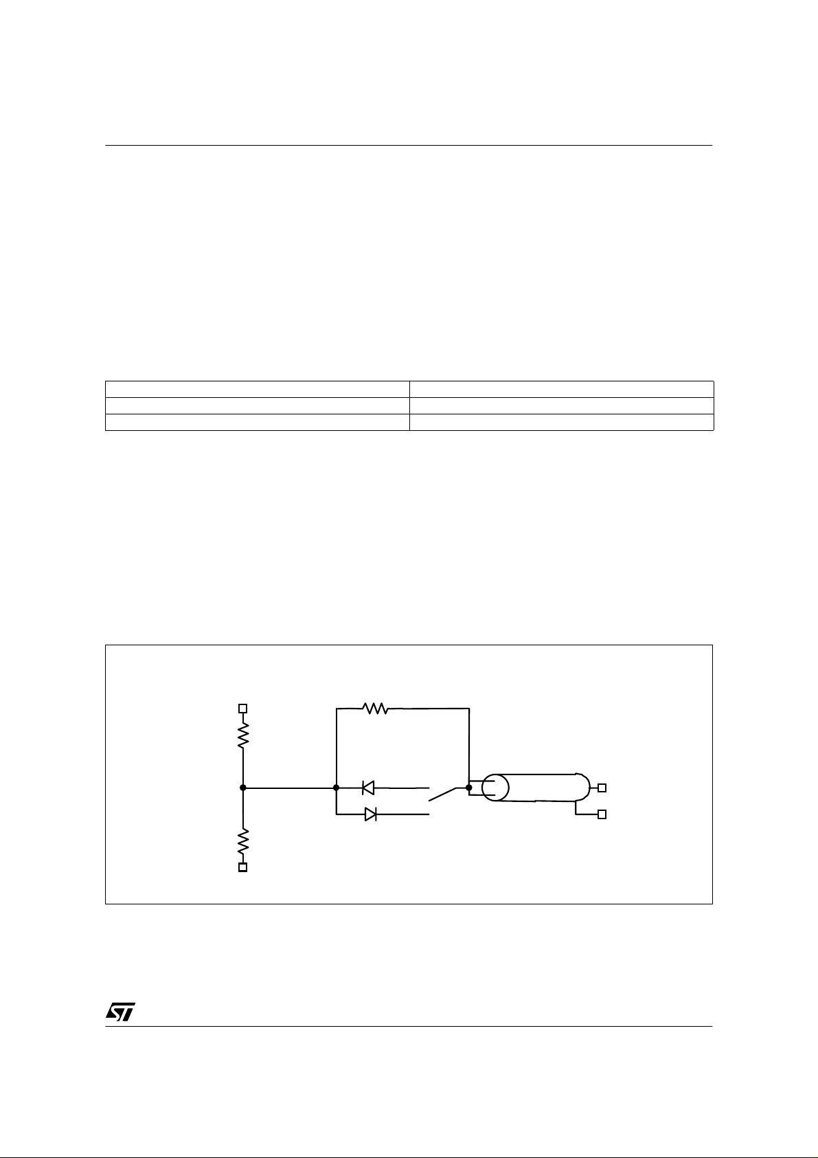
In this case to guar antee the r ight fre quency contro l, an R-C or R -C-D filter h as to be ins erted betwe en
the secondary winding and SEC (see figure 16).
The values of R 1f and C1f have to be c hosen in order to maintain the v oltage on SEC pin high er than
~0.9V during the fixed tON even if the voltage on the secondary winding becomes zero or negative.
On the other side it is important to have the SEC pin voltage higher than 2.2V before the end of the free-
wheeling diod e conduction to avoid delay at Power switch-ON. Therefor e the filter dimensioning is a
trade-off between the charge and the discharge time constant.
The circuit reported in figure 16b can be used if different and independent time constants are necessary.
DCbus
/2
Figure 16: External trigger circuits
C1f
SEC
SEC
VK06
VK06
a)
b)
R1f
C1f
R2f
R1f
Df
3.7 CONVERTER FOR COLD IGNITION APPLICATIONS (NO PRE-HEAT)
For applicati ons where the pre- heating of t he cathod es is no t reque sted, it is po ssib le to use a sim plifi ed
converter as reported in figure 17.
14/32

Obsolete Product(s) - Obsolete Product(s) Obsolete Product(s) - Obsolete Product(s)
Figure 17: Application circuit without preheat
AN1902 - APPLICATION NOTE
R14
C12
R1
C3
C10
C6
VCC
CAP2
CAP1
CapPREH
VCC
CAP2
CAP1
CapPREH
CapEOL
CapEOL
C8
COLL
COLL
DIAC
GND
DIAC
SEC
GND
SEC
DC BUS
Ls
Ls
R3
C4
C14
R10
Lp
C1
Tube
Cbulk
C2
4. VK06 Design Reference
This design reference has been developed to help the VK06 users in the application board development.
To point out the m aximum VK06 performa nces we decided to drive a 5 8W T8 FL tube. Two different
PCBs have been realized, the first on e using only su rface mounting com ponents and the seco nd one
using only through hole components. In the figure 18a, 18b, 18c their photos are shown.
15/32

Obsolete Product(s) - Obsolete Product(s) Obsolete Product(s) - Obsolete Product(s)
AN1902 - APPLICATION NOTE
Figure 18: VK06 demoboard: SMD components, top (a) and bottom (b) view; through-hole top view (c)
a)
b)
c)
4.1 Electrical scheme
In figures 19 and 20 th e electri cal sche mes for both tro ugh hole and s urface mou nting de moboards ar e
shown.
16/32

Obsolete Product(s) - Obsolete Product(s) Obsolete Product(s) - Obsolete Product(s)
Figure 19: Thro ugh hol e compone nts demoboar d electr ica l scheme
AN1902 - APPLICATION NOTE
M1
F1
R1
58W
C1
R4
C2
T1
R12
C13
R14
C12
R15
C11
C10
Dz2
4
7
VK06TLS
1
6
7
VK06TLS
4
1
6
C16
5
C15
5
C9
3
9
2
8
+
3
2
8
C14
R10
R8
C7
C8
+
R5
D1
Dz1
C4 C3
C5
R6
C6
17/32

Obsolete Product(s) - Obsolete Product(s) Obsolete Product(s) - Obsolete Product(s)
Figure 20: SMD demoboard electrical scheme
F1
AN1902 - APPLICATION NOTE
R1
M2
58W
C1
R2
C2
R3 R4
T1
R12
C13
R5
R14
R13
C12
C11
R15
R16
Dz2
6
4
5
6
4
5
9÷16
VK06TL
1 2
7
C15
C10
R18
9÷16
VK06TL
1
7
C16
R17
3
8
C9
3
8
2
C8
C14
R10
R9
R8
D1
Dz1
R6
C3
C4
C5
C7
C6
4.2. COMPONENTS LIST
The material lists for both PCB are reported in tables 1 and 2.
18/32

Obsolete Product(s) - Obsolete Product(s) Obsolete Product(s) - Obsolete Product(s)
AN1902 - APPLICATION NOTE
Table 1: Components list of the VK06 demoboard with trough hole components
Reference Value Description
R1
R4
R5, R12
R6
R8
R10, R14
R15
C1
C2
C3, C12, C8
C4
C5, C13
C6, C10, C15, C16
C7, C9
C11
C14
D1
Dz1
Dz2
T1
IC1, IC2
330kΩ 1/2W 5% 400V Resistor
1MΩ 1/2W 5% 400V Resistor
15kΩ 1/4W 5% Resistor
68kΩ 1/4W 5% Resistor
1MΩ 1/4W 5% Resistor
180kΩ 1/2W 5% 400V Resistor
2.2MΩ 1/2W 5% 400V Resis tor
8.2nF 2000V 5% Resonan t capacitor
100nF 400 V Capaci tor
330nF 16V 10% Capaci tor
47nF 50V 10 % Capacitor
100 pF 100 V 10% Capacitor
1nF 2% Capacitor
4.7µF 16V 20% Electrolytic capacitor
10nF 50V Capaci tor
1nF 630V Snubber capacitor
If=0.15A Vrrm=75V Rectifier diode
36V Zener diode
18V Zener diode
1.8 mH 10% Resonant Inductor Pulse Eld or 60010019
STMicroelectronics VK06TLS
THROUGH HOLE COMPONE NTS DEMOBOARD INDUCTOR SPECIFICATION
MECHANICAL DRAWING (Bottom view) MECHANICAL DRAWING
ELECTRICAL CONNECTION ELECTRICAL CHARACTERISTI CS
Nominal Inductance (W 1=1-8) L=1.8m H ± 10%
Core EC 28
Turn ratio = W1/W2=W1/W3=10
2 = Lamp;
3 = Ground;
4 = Low Side SEC pin;
5 = Not connected;
8 = High Side SEC pin;
9 = Not connected;
11 = Mid Point
19/32

Obsolete Product(s) - Obsolete Product(s) Obsolete Product(s) - Obsolete Product(s)
AN1902 - APPLICATION NOTE
Table 2: Components list of the VK06 demoboard with SMD components
Reference Value Description
R17,R18 R19,R20 0 Ω Zero ohm Resistor
R15,R16 1MΩ 200V 5% 200V Resistor 1206
R8 1MΩ 5% Resistor
R3,R4 470kΩ 5% 200V Resistor 1206
R1,R2 220kΩ 5% 0.25W 200V Resistor 1206
R9,R10 R13,R14 100kΩ 5% 0.25W 200V Resistor 1206
R5,R12 15kΩ 5% Resistor
R6 68kΩ 5% Resistor
C5,C13 100pF 10 0V 10% Capacitor
C6,C10 , C15,C16 1nF 2% 16V Capacitor
C7,C9 4.7uF 10% 16V Capacitor
C3,C8,C12 330nF10% 16V Capacitor
C11 10n F 50 V Capac itor
C4 4 7n F 50 V 10% Capac itor
C1 8. 2n F 5% 20 00 V Resonant capa ci t or
C2 100nF 40 0V Capacitor
C14 1nF 630V Snubber capacitor
D1 If=0.15A Vrrm=75V Rectifier diode
Dz1 36V Zener di od e
Dz2 18V Zener di od e
T1 1.8 mH 5%
IC1, IC2 STMicroelectronics VK06TL
Resona nt Inductor VO G T: LL 010 205 31
TDK: SRW2 5EVD4-E01H003.
SMD COMPONENTS DEMOBOARD INDUCTOR SPECIFICATION
MECHANICAL DRAWING (Bottom view) MECHANICAL DRAWING
ELECTRICAL CONNECTION ELECTRICAL CHARACTERISTI CS
Nominal Inductance (W 1=1-8) L=1.8m H ± 5%
Core EVD 25
Turn ratio = W1/W2=W1/W3=10
1 = Lamp;
2 = Ground
3 = Low Side SEC pin;
5 = High Side SEC pin;
8 = Mid point
20/32

Obsolete Product(s) - Obsolete Product(s) Obsolete Product(s) - Obsolete Product(s)
AN1902 - APPLICATION NOTE
4.3. PCB DEFINITION
In figures 21 and 22 the proposed PCB for both SMD and trough hole demoboards are shown.
Figure 21: SMD PCB Bottom view (not in scale)
Figure 22: Through hole PCB Bottom view (not in scale)
The componen ts placement on the PCB is important and few simple ru les have to be followed for its
realization.
1) Frequency capacitor placement:
These components must be connected as close as possible to the CAP1 pin.
2) Ground path:
The ground paths (signal and power) must be separate in order to reduce interference on the logic part.
In figure 23 an example of this rule is shown.
21/32

Obsolete Product(s) - Obsolete Product(s) Obsolete Product(s) - Obsolete Product(s)
AN1902 - APPLICATION NOTE
Figure 23: PCB Ground path
Signal Ground
Power Ground
4.4. EXPERIMENTAL RESULTS
For the board testing it is i mportant to connect on the input termina ls an electrolyti c capacitor (10µF,
450V), in order to bypass the parasitic inductance present in the connection wires between the DC
supply voltage and the board (see figure 24).
Figure 24: Connection between the DC supply voltage and the board
DC Power Supply VK06 Demoboard
All the measurements have been done supplying the converter with 400V DC.
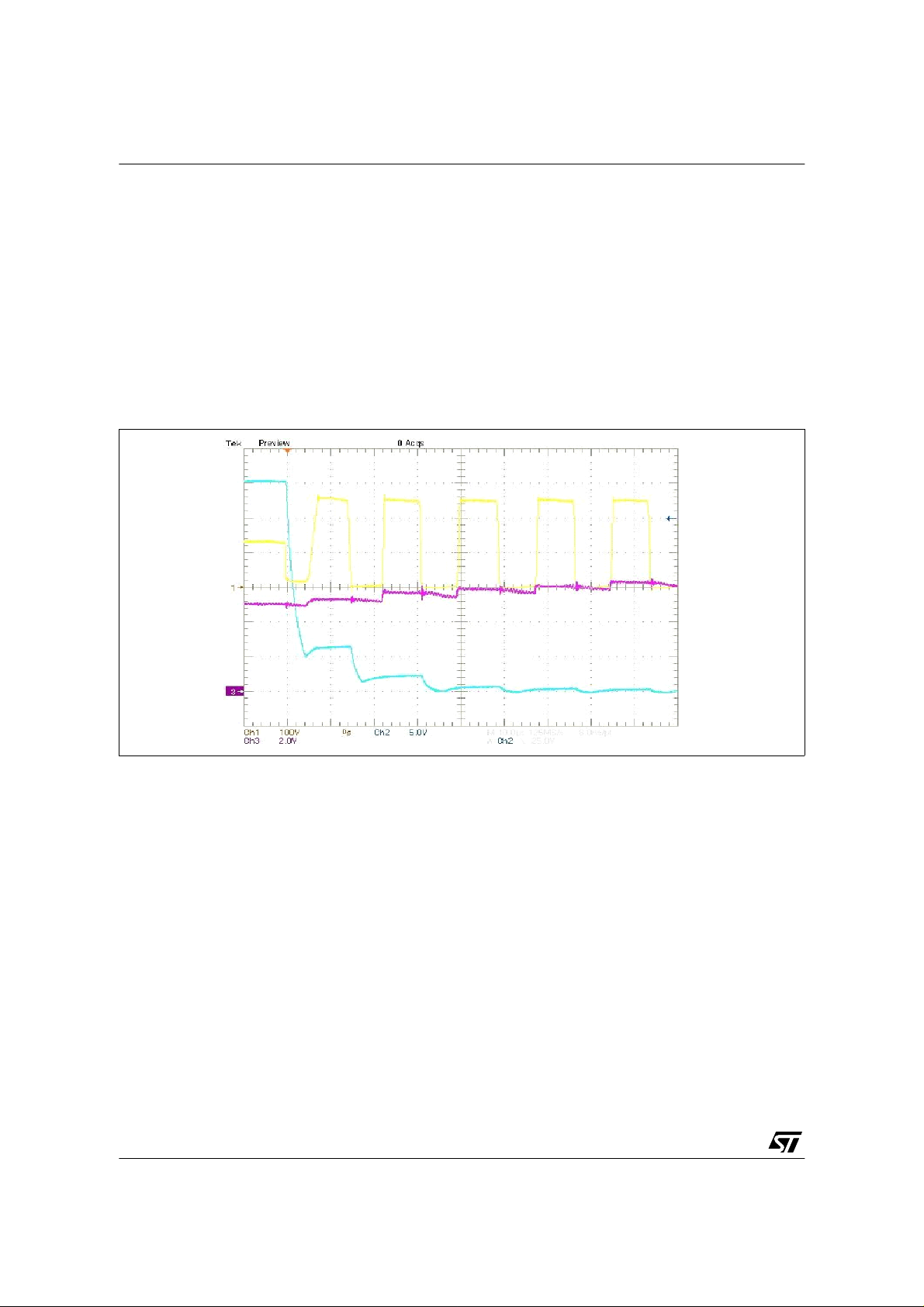
4.4.1 START-UP PHASE
In figure 25 the start-up phase is shown. The voltages on the low side (LS) VCC and diac pins are
reported.
It is possible to notice that th e VCC voltage reaches its cl amp value (~6.8V) before the dia c strike. In
figure 26 the first oscillation cycles after the diac strike are shown.
22/32

Obsolete Product(s) - Obsolete Product(s) Obsolete Product(s) - Obsolete Product(s)
Figure 25: Start-up phase
AN1902 - APPLICATION NOTE
LS DIAC pin voltage
LS VCC pin voltage
Figure 26: First oscillation cycles after the diac strike
LS colle ctor current
Mid point voltage
LS DIAC pin voltage
4.4.2 PRE-HEATING PHASE
The preheati ng frequen cy has to be fi xed in order to reach a cur rent le vel enough to h eat the catho des
without tube ignition. Figure 27 shows the main waveforms of the LS device.
LS VCC pin voltage
23/32

Obsolete Product(s) - Obsolete Product(s) Obsolete Product(s) - Obsolete Product(s)
Figure 27: Operation during the pre-heat
LS CAP1 pin voltage
AN1902 - APPLICATION NOTE
LS SEC pin voltage
The preheating frequency is ~59KHz with a peak current of ~800mA.
Being the reson ance capacitor C1= 8.2nF, d uring the preheat its voltage is lower th an the preheating
specification of a 58W T8 tube (350V peak).
Figure 28 shows the preheating timing. The choke current and the voltage on the CapPREH pin are
reported. The preheating duration is ~0.84s (C7=4.7uF)
Figure 28: Pre-heating phase timing
Choke current
Choke cu rrent
Mid point voltage
LS CapPREH pin voltage
24/32

Obsolete Product(s) - Obsolete Product(s) Obsolete Product(s) - Obsolete Product(s)
AN1902 - APPLICATION NOTE
4.4.3 IGNITION PHASE
Figure 29 shows the main waveform during the ignition phase. The peak current is limited to ~2A thanks
to the o vercur rent pr otec tion ne tw ork made by D1, Dz1 and R6 ( see figure s 19 and 20 ). In fact as soon
as the voltage on the sec pi n overcomes ~40V the frequen cy capacitors charge becomes faster (see
CAP1 waveform) anticipating the device switch-off.
Figure 29: Igni tion phase
LS CAP1 pin voltage
LS SEC pin voltage
Choke current
Mid point voltage
4.4.4 STEADY STATE
Figure 30 shows the steady state phase main waveforms. The working frequency is ~34KHz with a peak
current of ~700mA.
Figure 30: Steady state phase
LS CAP1 pin voltage
LS SEC pin voltage
Choke current
Mid point voltage
25/32

Obsolete Product(s) - Obsolete Product(s) Obsolete Product(s) - Obsolete Product(s)
4.5 PROTECTIONS
4.5.1 End of Life
In figure 31 the timing of the EoL protection is shown.
Figure 31: End Of Life timing
Choke cur ren t
AN1902 - APPLICATION NOTE
The system oper ates as follows: after the start-up, the prehe ating phase starts an d l asts ~0.84 s ec as in
the normal opera tion. After the prehe ating phase the system could perma nently work in free oscilla tion
condition due to the EoL state. The protection stops the oscillation after ~50msec.
Figure 32: EoL: device turn-off
Choke current
LS CapPREH pin voltage
Mid point voltage
26/32
Obsolete Product(s) - Obsolete Product(s) Obsolete Product(s) - Obsolete Product(s)
AN1902 - APPLICATION NOTE
Figure 32 shows the particular of the LS device turn-off when the voltage on the LS CapPREH pin
reaches the internal threshold.
4.6 THERMAL EVALUATION
The thermal analysis has been performed measuring the devices temperatures in the SMD version
demoboard. The heat sink copper area copper area is ~100mm2 for each device.
The temperature has been measured with K type thermocouples put on the top of the SO-16 packages.
The measurements have been performed at two different ambient temperatures: room temperature
(about 25°C) and 50°C. The results are summarized in table 3.
Table 3: Devices temperature
T
ambient
25ºC 90ºC
50ºC 115ºC
5. TUBE RECTIFICATION (not included in the reference demoboards)
Below, a network for the r ectification detec tion is described. Th e dimensioning is related to a 58W T 8
tube. This is an anomalous condition happening during the steady state phase causing lamp overvoltage
and not overcurrent, for this reasons it is not possible to detect it by the EoL protection.
The propos ed network realizes a lam p voltage sense. The timing and the device l atch is realiz ed using
the same internal EoL circuit.
The circuit used to simulate the rectification condition has been realized according to E DIN IEC 61347-23/A1 2002-02 standard (see figure 33).
T
case
Figure 33: Circuit for simulating the rectifying effects
C
R1
5.6
5W
5.6
R2
5W
E
The points C,D,E,F must be connect to the VK06 converter output terminals.
R1
100 10W
D2
2 x BYV228
D1
2 x BYV228
Tube T8 58W
D
F
In figure 34 the circuit used for the tube rectification detection is shown.
27/32

Obsolete Product(s) - Obsolete Product(s) Obsolete Product(s) - Obsolete Product(s)
Figure 34: Proposed circuit for detecting the rectifying effects
AN1902 - APPLICATION NOTE
EOL Pin
Mid Point
27k
C
E
T1
1.8mH
R
DZ
33V
D
0.2A, 75V
470 pF 630V
C
560k
R
R 180k
C2
100 nF
C1
8.2nF
D
DC Bus = 400V
F
The terminals C-E and D-F must be connected to the circuit of figure 33.
The rectification condition is detected monitoring the voltage across the 180kΩ resistor.
When the rectifying effects occur, the increase of the voltage across the lamp causes the increase of the
voltage across the resistor R= 180kΩ over the threshold fixed by the network D-Dz-R. At that moment the
EoL protection is activated.
During the preheating phase the voltage across the resistor R=180kΩ is higher than the steady state and
the protect ion can be activ ated. For this reason a further circuit is n eeded for disa bling the prote ction
during the preheat.
6. CONVERTER FREQUENCY TOLERANCE VS. FREQUENCY CAPACITOR TOLERANCE
Following a practical example showing the variation of converter frequency versus the frequency
capacitor tolerance.
The analysis has been performed in steady state condition but it is also applicable to the pre-heat.
A VK06TL based prototype board with the following setting has been used:
VDC bus= 350V
C
freqLS
= C
=C=1.22 nF (measured)
freqHS
Figure 35 shows the related steady state waveforms.
28/32

Obsolete Product(s) - Obsolete Product(s) Obsolete Product(s) - Obsolete Product(s)
AN1902 - APPLICATION NOTE
Figure 35: Test condition: C
LS collector current
Following the measured parameters:
f=52.2KHz
duty cycle ≈ 50%
P=45.5W
With:
t
= t
ONLS
t
storageLS
dv/dt=920ns
ONHS
= t
storageHS
= 8.36µs
=320ns
= C
freqLS
Mid point voltage
freqHS
HS colle c tor current
LS CAP1 pin vol tage
According to the theoretical relationship:
tON=K*C with K=6.7µs/nF (5% internal guaranteed) (1)
The expected tON is:
tON= 6.7*1.22=8.2µs (inside 5% device tolerance)
- Experiment 1
Only the frequency capacitors have been changed:
C
=C+6%
freqLS
C
Figure 2 shows the related waveforms.
freqHS
=C-6%
29/32

Obsolete Product(s) - Obsolete Product(s) Obsolete Product(s) - Obsolete Product(s)
Figure 36: Test condition: 6% opposite variation on Cfreq
AN1902 - APPLICATION NOTE
LS collector current
Mid point voltage
Following the measured parameters:
frequency f=52.12KHz
duty cycle ≈ 47.4%
P=45.5W
With:
t
=8.8µs (+6%)
ONLS
t
=7.72µs (-6%)
ONHS
t
storageLS
dv/dt=920ns
= t
storageHS
= 320ns
HS colle c tor current
LS CAP1 pin vol tage
It means tha t the opp osite va riation of the tON causes a distortion of the duty cycle without var iation on
the frequency and power.
- Experiment 2
C
=C+6%
freqLS
C
Figure 37 shows the related waveforms.
freqHS
=C+6%
30/32

Obsolete Product(s) - Obsolete Product(s) Obsolete Product(s) - Obsolete Product(s)
Figure 37: Test condition: +6% variation on Cfreq
AN1902 - APPLICATION NOTE
LS colle ctor current
Mid point voltage
Following the measured parameters:
f=49.8KHz
duty cycle ≈ 50%
P= 46.2W
With:
T
= T
onLS
T
storageLS
dv/dt=920ns
=8.8µs (+6%)
onHS
= t
storageHS
=320ns
HS colle ct or current
LS CAP1 pin voltage
The frequency variation respect to the initial condition (C
than the capacitor tolerance (6%). The power variation is instead ~1.6%.
According to the rel atio nshi p ( 1), the sa me results can be ob tained i f the tON variation is c au sed on l y by
VK06TL internal tolerance. The worst case frequency variation will be anyway less than 5%.
freqLS
= C
= 1.22 nF) is 4.6% and it is less
freqHS
31/32

Obsolete Product(s) - Obsolete Product(s) Obsolete Product(s) - Obsolete Product(s)
AN1902 - APPLICATION NOTE
Information furnished is believed to be accurate and r eliable. However, STMicroelect r onics assumes no responsibility for the consequences
of use of such information nor for any infringement of patents or other rights of third parties which may results from its use. No license is
granted by implication or otherwi s e under any patent or patent rights of STMicroel ec tronics. Specificat ions mentioned in this publication are
subject to c hange without notic e. This publicatio n s upersedes and rep lac es all information previously supplied. STMicroelec tronics products
are not authorized for use as critical components in life support devices or systems without express written approval of STMicroelectronics.
The ST logo is a tr ademark of STMicroelectronics.
All other names are the property of their r es pective owners
2004 STMicroelectronics - Prin ted in ITALY- All Rights Reserved.
Australia - B elgium - Brazil - Canada - China - Czech Republic - Finland - France - German y - Ho ng K ong - India - Israel - Ital y - Japan -
Malaysia - Malta - Morocco - Singapore - Spain - Sweden - Switzerland - United Kingdom - United States
STMicroelectronics GROUP OF COMPANIES
http://www.st.com
32/32
 Loading...