

Page 1
AN1900
Slave
Board
DALI
Master
Board
Ballast
DALI S
Software
s
Slave
Board
Ballast
DALI
Master
Application note
Hardware implementation for ST7DALI-EVAL
Introduction
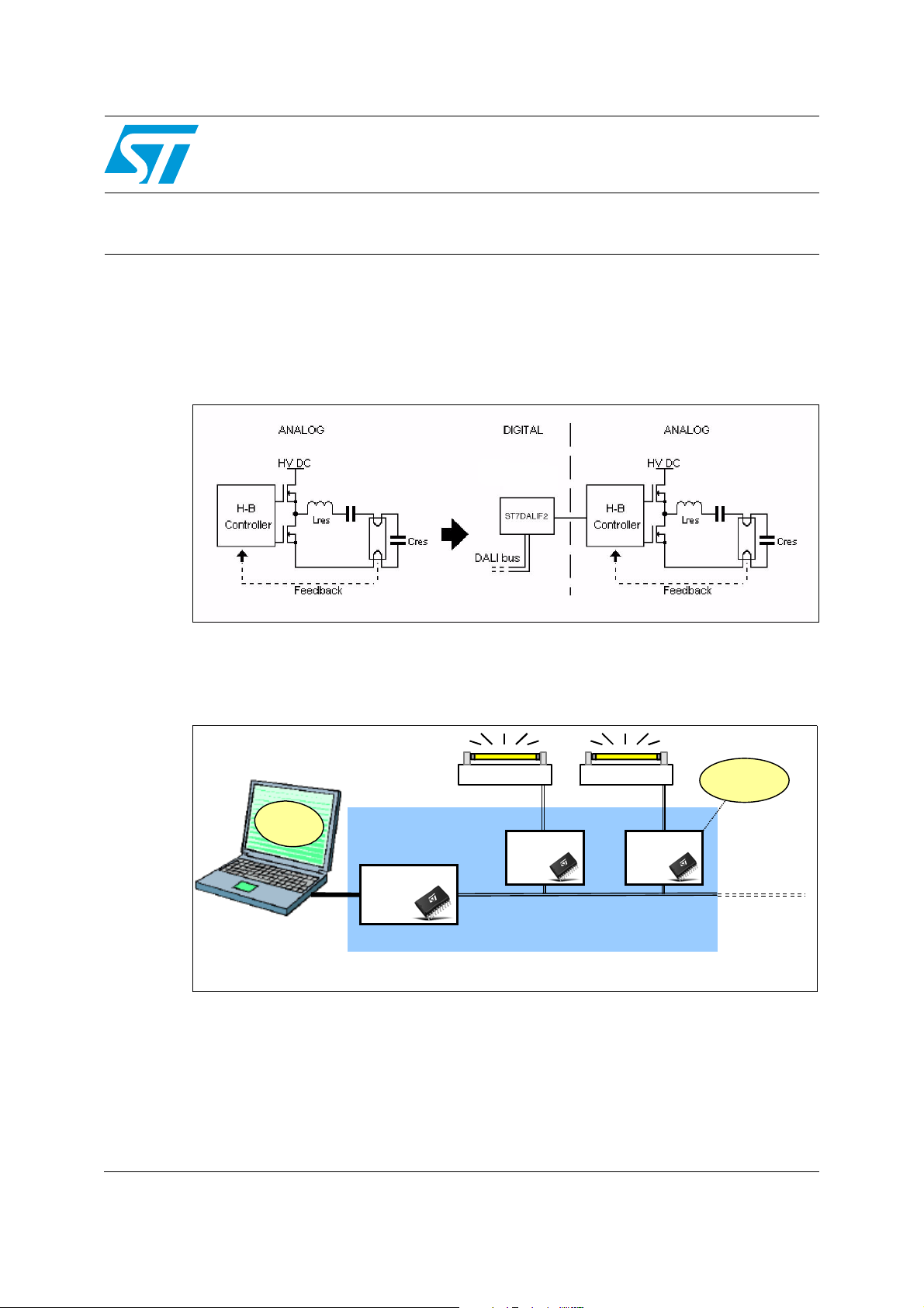
This application note describes how to implement a DALI (Digital Addressable Lighting
Interface) in an existing high-frequency dimmable tube-lamp ballast application.
Figure 1. Hardware overview with MCU handling only DALI communication
If necessary, please refer to Application Note AN1756 “Choosing a DALI implementation
Strategy with ST7DALIF2” for further background. This application note is issued with the
ST7DALI evaluation board which can be purchased with the sales type ST7DALI-EVAL.
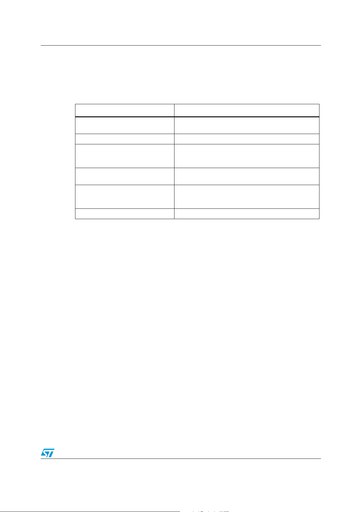
Figure 2. ST7DALI-EVAL principle
lave
1-10 V
DALI
1-10 V
DALI
Up to 64 slave
DALI Evaluation Kit
Please refer to the ST7DALI-EVAL Evaluation Kit user manual.
March 2009 Rev 2 1/11
www.st.com
Page 2

Contents AN1900
Contents
1 Hardware . . . . . . . . . . . . . . . . . . . . . . . . . . . . . . . . . . . . . . . . . . . . . . . . . . 3
1.1 ST7DALIF2 features . . . . . . . . . . . . . . . . . . . . . . . . . . . . . . . . . . . . . . . . . . 3
1.2 Interface between microcontroller and analog half-bridge controller . . . . . 3
1.3 Handling DALI reception and transmission with DCM peripheral . . . . . . . . 4
1.4 Power consumption considerations . . . . . . . . . . . . . . . . . . . . . . . . . . . . . . 4
2 Schematics and PCB . . . . . . . . . . . . . . . . . . . . . . . . . . . . . . . . . . . . . . . . 7
2.1 Schematics . . . . . . . . . . . . . . . . . . . . . . . . . . . . . . . . . . . . . . . . . . . . . . . . . 7
2.2 PCB . . . . . . . . . . . . . . . . . . . . . . . . . . . . . . . . . . . . . . . . . . . . . . . . . . . . . . 9
2.3 Bill of material . . . . . . . . . . . . . . . . . . . . . . . . . . . . . . . . . . . . . . . . . . . . . . . 9
3 Revision history . . . . . . . . . . . . . . . . . . . . . . . . . . . . . . . . . . . . . . . . . . . 10
2/11
Page 3
AN1900 Hardware
1 Hardware
1.1 ST7DALIF2 features
Table 1. List of requirements for the microcontroller
Minimum requirements ST7DALIF2 features
26 bytes of EEPROM, to save nonvolatile parameters
3 Kbytes program memory 8 Kbytes Flash program memory
A timer with Input Capture/Output
Compare capabilities to receive and
transmit DALI signals.
Low-consumption mode, to save
energy between commands.
I/Os and PWM outputs to perform the
interface with the ballast controller.
A clock source Internal 1% RC oscillator,
256 bytes data internal EEPROM
DALI communication module (DCM).
Halt power saving mode
Up to 15 multi-functional I/Os, one 12-bit Auto-reload
Timer with 4 PWM outputs, input capture and output
compare functions
In addition to DALI protocol handling, but without fully controlling the ballast, the
microcontroller can also monitor or customize some ballast parameters, for example for
easy calibration of various power levels in the factory, and/or act as a supervisor of the
complete ballast parameters.
1.2 Interface between microcontroller and analog half-bridge controller
A potential hardware problem is the interface between the microcontroller and the analog
half-bridge controller. One possibility is to use PWM outputs and to filter them to create
analog setpoints for the half-bridge controller. The 4 PWM outputs of the Autoreload timer
enable ST7DALIF2 to act on up to 4 different “external parameter” pins of the half-bridge
controller, for example L6574, without computation load (Please refer to AN993: L6574 &
Microcontroller in ballast applications). The designer is then in total control of the lamp.
Another easier solution is to keep the 1-10 V input widely used for dimming level control, and
use the microcontroller as a “gateway” or interface between the DALI bus and the analog
input of a conventional analog dimmable ballast. The microcontroller is then no longer in
direct connection with the analog ballast controller.
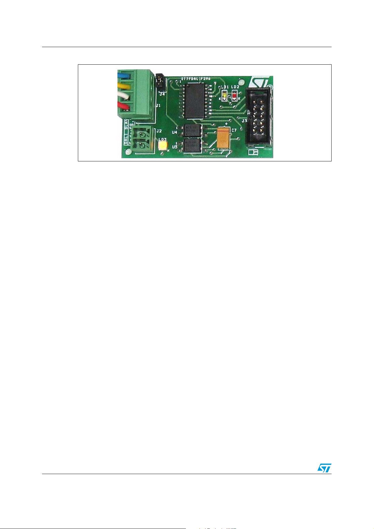
Based on this topology, a DALI master board based on the ST72F334J4 has been built and
a DALI slave board based on the ST7DALIF2 has been developed and can be seen in
Figure 3.
3/11
Page 4
Hardware AN1900
Figure 3. ST7DALI-EVAL DALI slave evaluation board
1.3 Handling DALI reception and transmission with DCM peripheral
The major embedded feature of the ST7DALIF2 microcontroller is the DALI Communication
Module (DCM). It allows decoding of the DALI forward frame and sending of the backward
frame, without any CPU overhead, or need for a timer with Input Capture or Output
Compare capabilities. It simplifies the software, saves processing time, and eases interrupt
management. The DCM drivers can be found in the ST7 Software Library or in the AN1601
Software Implementation for ST7DALI-EVAL.
1.4 Power consumption considerations
One of the biggest issues when designing a DALI ballast is the power supply of the
microcontroller when the lamp is off. When the lamp is on, supplying all devices can be quite
easily done via a charge pump taken from the middle point of the half-bridge. But in standby, the microcontroller should always be powered-on and ready to receive a DALI command.
This energy can only come from the mains. The current taken should then be as low as
possible to avoid constant dissipation. ST7DALIF2 has a power saving mode called “halt”,
using the smallest power consumption, since everything inside the MCU (core, peripherals
and clock source) is “frozen”. After entering this mode, only a reset or an external interrupt
can wake up the microcontroller. The interrupt can be triggered by the first (falling) edge of
the DALI frame. When this happens, Run mode is not immediately operational, mainly
because of the stabilization time of the clock source. This time has to be short enough to be
able to detect the second (rising) edge of a DALI frame. The first (falling) edge is not
significant but helps to wake up from Halt mode. Figure 4 shows, on channel 1, the DALI
frame on the DALI IN pin of the microcontroller, a pulse on channel 3 shows the beginning of
the run mode, and a high level on channel 4 shows that a proper DALI frame has been
received, and that the data is ready to be handled by the software.
4/11
Page 5

AN1900 Hardware
Figure 4. Overview of a forward frame reception
To better understand how the ST7DALIF2 can wake up fast enough, a zoom on the first
edge is needed, as shown in Figure 5.
Figure 5. Zoom on the first edges
When the first falling edge is detected, the microcontroller leaves Halt mode for a transition
period of 256 clock cycles. At 8 MHz, this means around 32 µs. Since the DCM starts
sampling 125 µs (worst case) after the falling edge, the microcontroller frequency can be
reduced to 4 MHz (i.e. 64 µs to wake up from halt). Although the software can work at 1 MHz
and still comply fully with DALI, it is then not possible to use Halt mode for additional power
saving at this frequency because the wake up is not fast enough to catch the beginning of
the incoming frame.
When the lamp is off, the microcontroller is not the only source of power dissipation. The
hardware interface between the DALI bus and the microcontroller also takes quite some
current, as shown in Figure 6.
5/11
Page 6

Hardware AN1900
Figure 6. DALI Bus- ST7DALIF2 interface
When the bus is high (steady state), 500 µA is always flowing through the resistor. Because
the microcontroller should always know if the bus is constantly low (bus failure), an
alternative and more power-saving topology is not possible. On the one hand, current in the
resistor should be as low as possible, but on the other hand it should not be so low that any
noise fools the microcontroller. When the transistor turns off, the current should be high
enough to evacuate the carriers within the right time frame. 10 kohms is a good trade-off
(please refer to the I/O ports section of the ST7DALIF2 data sheet).
Here is a summary, depending on the frequency chosen:
Table 2. Power consumption overview
Halt Mode Run Mode
(f
run=4 MHz) (f
CPU
Interface 500 µA 500 µA
ST7DALIF2 10 µA 2.7 mA
Total @5V 170 mW 890 mW
run=1 MHz)
CPU
Finally, the accuracy of the ST7DALIF2 ADC is directly proportional to the VDD regulation
accuracy. If the microcontroller supply is regulated with a standard zener diode for example,
the ADC precision would be around 10%. If precise measurements have to be performed,
then a voltage regulator with low quiescent current and high precision is needed, typically
from the LD2980 series.
6/11
Page 7

AN1900 Schematics and PCB
2 Schematics and PCB
2.1 Schematics
Aside from the ST7DALIF2 microcontroller itself, the ST7DALI-EVAL DALI Slave board has
four main sections: Power Supply, DALI Bus-ST7DALIF2 Interface, In-Circuit
Communication, 1-10 V Interface (see Figure 7).
The power supply section is very simple. A LD2980 provides an accurate 5V output, while
jumper 4 allows you to easily measure the current used by the power supply, the
microcontroller and the interface with the DALI Bus.
The bridge diode protects the DALI Bus-ST7DALIF2 interface against wrong polarity wiring
however it is not protected from over-voltage from accidental mains connection between the
control wires. For such protection, a high voltage switch is needed.
Since the DALI Protocol specifies that isolation is required, two optocouplers are needed:
one for transmission (U4) and one for the reception (U5). For cost reasons, the transmission
optocoupler cannot sustain the 250 mA required to pull the DALI bus down (it is high in
steady state), so a power stage has to be implemented via Q1. For the bus to be kept down
during transmission, capacitor C7 is used since a voltage must remain on the base of Q1. To
avoid a discharge of this capacitor via the optocoupler U5, the diode D6 is required.
Finally the zener diode D5 is used to ensure that the wide voltage specifications of the DALI
bus (High level: 9.5 to 22.5 V. Typical 16 V. Low level: -6.5 to +6.5 V. Typical 0 V) can be
fulfilled.
The ST7 In-Circuit Communication (ICC) allows In-Circuit Programming (ICP) and InApplication Programming (IAP). Please refer to the Flash program memory section of the
ST7DALIF2 datasheet.
A standard dimmable ballast can be easily driven through the evaluation board with the 110 V Interface. A PWM with programmable duty cycle is generated by the ST7DALIF2,
filtered to a DC value proportional to the duty cycle, and amplified from 0-5 V to 1-10 V
through to the operational amplifier U2A.
Regardless of whether a ballast is available or not, the LED LD3 gives an overview of the
light level.
7/11
Page 8

Schematics and PCB AN1900
Figure 7. ST7DALI-EVAL DALI slave schematic
8/11
Page 9

AN1900 Schematics and PCB
2.2 PCB
The PCB has been designed to look like the add-on to an existing ballast design (see
Figure 8). Gerber files are delivered with the ST7DALI-EVAL kit.
Figure 8. EVAL6574 and ST7DALI-EVAL evaluation boards together
2.3 Bill of material
Please refer to the ST7DALI-EVAL User Manual.
9/11
Page 10

Revision history AN1900
3 Revision history
Table 3. Document revision history
Date Revision Changes
31-May-2004 1 Initial release.
17-Mar-2009 2 Changed product references from ST7DALI to ST7DALIF2.
10/11
Page 11

AN1900
Please Read Carefully:
Information in this document is provided solely in connection with ST products. STMicroelectronics NV and its subsidiaries (“ST”) reserve the
right to make changes, corrections, modifications or improvements, to this document, and the products and services described herein at any
time, without notice.
All ST products are sold pursuant to ST’s terms and conditions of sale.
Purchasers are solely responsible for the choice, selection and use of the ST products and services described herein, and ST assumes no
liability whatsoever relating to the choice, selection or use of the ST products and services described herein.
No license, express or implied, by estoppel or otherwise, to any intellectual property rights is granted under this document. If any part of this
document refers to any third party products or services it shall not be deemed a license grant by ST for the use of such third party products
or services, or any intellectual property contained therein or considered as a warranty covering the use in any manner whatsoever of such
third party products or services or any intellectual property contained therein.
UNLESS OTHERWISE SET FORTH IN ST’S TERMS AND CONDITIONS OF SALE ST DISCLAIMS ANY EXPRESS OR IMPLIED
WARRANTY WITH RESPECT TO THE USE AND/OR SALE OF ST PRODUCTS INCLUDING WITHOUT LIMITATION IMPLIED
WARRANTIES OF MERCHANTABILITY, FITNESS FOR A PARTICULAR PURPOSE (AND THEIR EQUIVALENTS UNDER THE LAWS
OF ANY JURISDICTION), OR INFRINGEMENT OF ANY PATENT, COPYRIGHT OR OTHER INTELLECTUAL PROPERTY RIGHT.
UNLESS EXPRESSLY APPROVED IN WRITING BY AN AUTHORIZED ST REPRESENTATIVE, ST PRODUCTS ARE NOT
RECOMMENDED, AUTHORIZED OR WARRANTED FOR USE IN MILITARY, AIR CRAFT, SPACE, LIFE SAVING, OR LIFE SUSTAINING
APPLICATIONS, NOR IN PRODUCTS OR SYSTEMS WHERE FAILURE OR MALFUNCTION MAY RESULT IN PERSONAL INJURY,
DEATH, OR SEVERE PROPERTY OR ENVIRONMENTAL DAMAGE. ST PRODUCTS WHICH ARE NOT SPECIFIED AS "AUTOMOTIVE
GRADE" MAY ONLY BE USED IN AUTOMOTIVE APPLICATIONS AT USER’S OWN RISK.
Resale of ST products with provisions different from the statements and/or technical features set forth in this document shall immediately void
any warranty granted by ST for the ST product or service described herein and shall not create or extend in any manner whatsoever, any
liability of ST.
ST and the ST logo are trademarks or registered trademarks of ST in various countries.
Information in this document supersedes and replaces all information previously supplied.
The ST logo is a registered trademark of STMicroelectronics. All other names are the property of their respective owners.
© 2009 STMicroelectronics - All rights reserved
STMicroelectronics group of companies
Australia - Belgium - Brazil - Canada - China - Czech Republic - Finland - France - Germany - Hong Kong - India - Israel - Italy - Japan -
Malaysia - Malta - Morocco - Singapore - Spain - Sweden - Switzerland - United Kingdom - United States of America
www.st.com
11/11
 Loading...