

Page 1

AN1895
Application note
EVAL6562-375W Evaluation Board
L6562-based 375W FOT-controlled PFC Pre-regulator
Introduction
This application note describes a 375W evaluation board based on the L6562 Transitionmode Power Factor Correction (PFC) controller (order code: EVAL6562-375W).
The board implements a 375W, wide-range mains input, PFC pre-regulator that is suitable
for a 300/350W ATX12V power supply unit (PSU).
To enable the use of a low-cost device like the L6562 at a power level that is usually
prohibitive for this device, the chip operates with a Fixed-Off-Time (FOT) control system.
This allows Continuous Conduction Mode operation, normally achievable with more
expensive control chips and more complex control architectures.
EVAL6562-375W evaluation board
August 2006 Rev 3 1/16
www.st.com
Page 2

Contents AN1895
Contents
1 Board description . . . . . . . . . . . . . . . . . . . . . . . . . . . . . . . . . . . . . . . . . . . 3
2 Power stage design procedure . . . . . . . . . . . . . . . . . . . . . . . . . . . . . . . . 5
3 Setting up FOT control with the L6562 . . . . . . . . . . . . . . . . . . . . . . . . . . 7
4 Getting started with the evaluation board . . . . . . . . . . . . . . . . . . . . . . . 9
4.1 Testbench results and significant waveforms . . . . . . . . . . . . . . . . . . . . . . . 9
5 References . . . . . . . . . . . . . . . . . . . . . . . . . . . . . . . . . . . . . . . . . . . . . . . . 12
Appendix A Bill of materials . . . . . . . . . . . . . . . . . . . . . . . . . . . . . . . . . . . . . . . . . 13
Revision history . . . . . . . . . . . . . . . . . . . . . . . . . . . . . . . . . . . . . . . . . . . . . . . . . . . . 15
2/16
Page 3
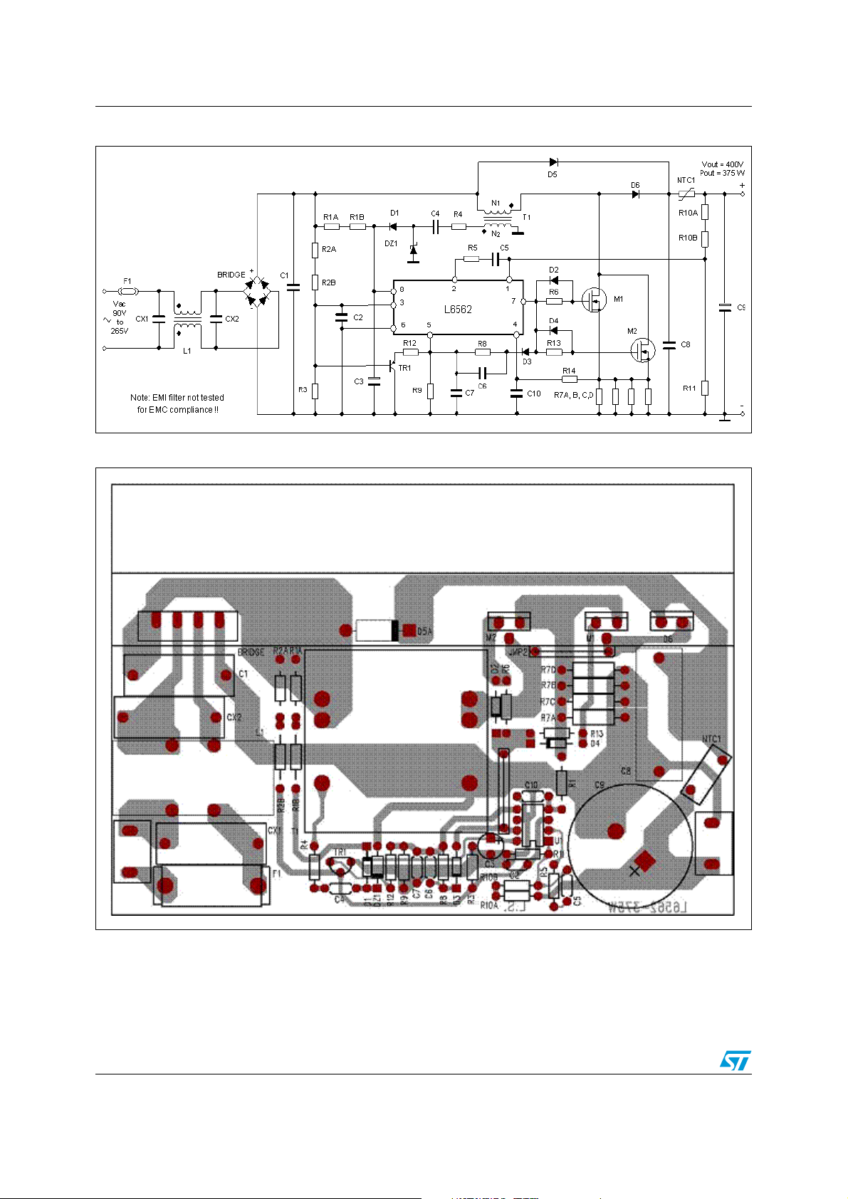
AN1895 Board description
1 Board description
The EVAL6562-375W evaluation board includes a Power Factor Correction (PFC) preregulator for a 300W ATX 12V power supply unit (PSU). It is able to deliver 375W continuous
power on a regulated 400V rail from a wide range of mains voltage. This rail will be the input
for the cascaded isolated DC-DC converter (typically a forward converter) that will provide
the output rails of the silver box. Although the ATX specification envisages air cooling,
typically realized with a fan capable of an airflow in the range of 25-35 CFM, this is not
allowed for in the design of this evaluation board. Enough heat sinking will be provided to
allow full-load operation in still air. With an appropriate airflow and without any change in the
circuit, the evaluation board can easily deliver up to 400-420W.
The L6562 controller chip is designed for Transition-Mode (TM) operation where the boost
inductor works next to the boundary between Continuous (CCM) and Discontinuous
Conduction Mode (DCM). However, with a slightly different usage, the chip can operate so
that the boost inductor works in CCM, hence surpassing the limitations of TM operation in
terms of power handling capability. The gate-drive capability of the L6562 (±0.8A min.) is
also adequate to drive the MOSFETs used at higher power levels.
This approach, which couples the simplicity and cost-effectiveness of TM operation with the
high-current capability of CCM operation, is the Fixed-Off-Time (FOT) control. The control
modulates the ON-time of the power switch, while its OFF-time is kept constant. More
precisely, it will be used the Line-Modulated FOT (LM-FOT) where the OFF-time of the
power switch is not rigorously constant but is modulated by the instantaneous mains
voltage. Please refer to [2] for a detailed description of this technique.
Ta bl e 1 summarizes the electrical specification of the application and Ta ble 3 lists
transformer specifications.
The electrical schematic is shown in Figure 1 and the PCB layout in Figure 2.
Appendix A lists the bill of materials.
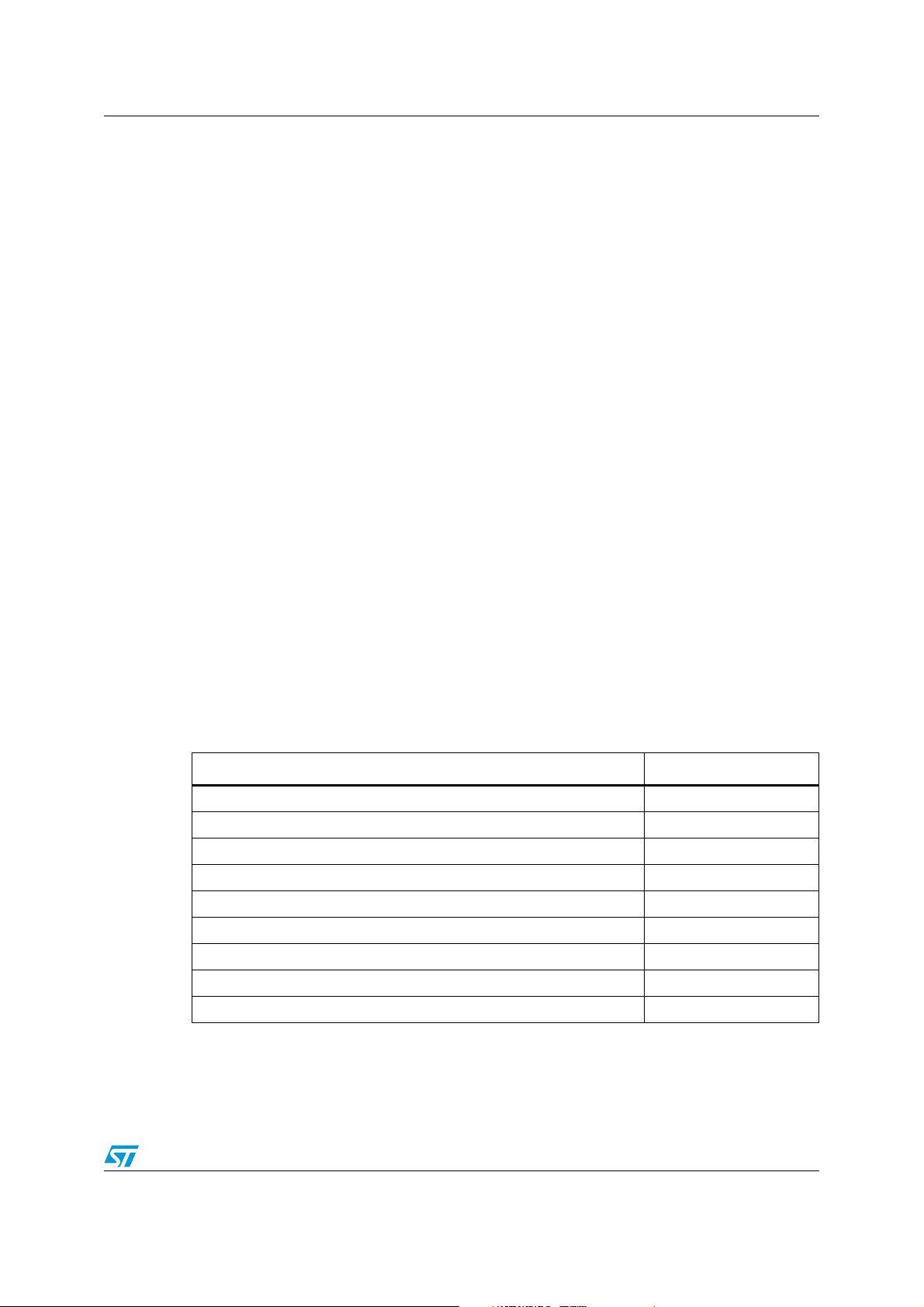
Table 1. Electrical specifications
Parameter Value
Line voltage range 90 to 265 V
Minimum line frequency (fL)47 Hz
Regulated output voltage 400 V
Rated output power 375 W
Maximum 2f
Hold-up time 17 ms
Maximum switching frequency (@ V
Minimum estimated efficiency (@ V
Maximum ambient temperature 50° C
output voltage ripple 20V pk-pk
L
= 90 VAC, P
IN
= 90 VAC, P
IN
= 375 W) 100 kHz
OUT
= 375W) 90%
OUT
AC
3/16
Page 4
Board description AN1895
Figure 1. Electrical schematic diagram
Figure 2. PCB layout, silk + bottom layer (top view) (150 x 81.5 mm)
4/16
Page 5

AN1895 Power stage design procedure
2 Power stage design procedure
The step-by-step procedure of an LM-FOT controlled PFC pre-regulator outlined in [2] will
be followed. The design will be done on the basis of a ripple factor (the ratio of the maximum
current ripple amplitude to the inductor peak current at minimum line voltage) Kr=0.3.
1. The range of k (k
Vin
k
min
---------------------------------- -
2
÷ k
min
(RMS)min
Vout
) associated to the line voltage range is:
max
2
90
--------- -
400
0.318, k
max
Vin
(RMS)max
------------------------------------
2
Vout
2
265
--------- -
400
0.937======
.
2. The required t
frequency (on the top of the line voltage sinusoid) f
3. The maximum expected input power Pin
Ipk
are:
max
Pin
is derived from the specification on the maximum switching
OFFmin
t
OFFmin
375
--------- - 417W; Ipk
0
0.9
k
min
-------------------
f
sw max
max
0.318
----------------------- - 3.18µs== =
⋅
100 10
= Pout0/η and the maximum line peak current,
0
2Pin
0
-------------------------
k
Vout
min
at minimum line voltage:
swmax
3
2417⋅
----------------------------- 6.56A== = = =
0.318 400⋅
.
4. The ripple amplitude on the top of the sinusoid at minimum line voltage, assuming it is
75% of the maximum specified, will be:
Lpk
------------------ -
83Kr–
Ipk
max
I
∆
6Kr
60.3⋅
-------------------------
830.3⋅–
6.56⋅ 1.66A== =
5. The required inductance L of the boost inductor is:
L1k
–()
min
Vout
------------- -
I
∆
Lpk
t
OFFmin
400
1 0.318–()
-----------
⋅⋅⋅ 523µH== =
1.66
3.18 10
6–
This value will be rounded up to 550 µH; the resulting value of Kr will be slightly smaller
than 0.3, but we will go on using the target value, this will give some additional margin.
6. The maximum inductor peak current, I
8
I
Lpkmax
------------------ -
83Kr–
lpk
max
, is calculated:
Lpkmax
-------------------------
830.3⋅–
8
6.56⋅ 7.39A== =
7. The maximum sense resistor R
R
sense max
sensemax
is:
1.6
-------------------- -
I
Lpkmax
1.6
----------- 0.216Ω===
7.39
(1.6V is the minimum value of the pulse-by-pulse current limiting threshold on the
current sense pin of the L6562). It will be realized with four 0.68Ω, 1W-rated paralleled
resistors, for a total resistance of 0.17Ω. This provides some extra power capability. The
inductor peak current that the inductor must be able to carry without saturating will be:
I
Lpksat
1.8
----------- 10.6A==
0.17
8. From the formulae in [2], table 4, the MOSFET RMS current is:
I
Qrms()
Pin
0
-------------------------
k
Vout
min
16k
min
2
------------------ -–
3 π⋅
417
-----------------------------
0.318 400⋅
16 0.318⋅
2
------------------------- -– 3.96A== =
3 π⋅
5/16
;
Page 6

Power stage design procedure AN1895
The diode RMS current is:
Pin
I
Qrms()
-------------------------
k
min
The dissipation on the sense resistor will be 0.17·3.96
0
Vout
16k
min
------------------ -
3 π⋅
417
-----------------------------
0.318 400⋅
16 0.318⋅
------------------------- - 2.41A== =
3 π⋅
2
=2.7W, which justifies the use of
four resistors; the selected MOSFET is the STP12NM50, a 0.3Ω/500V MDmesh™ type
from STMicroelectronics, housed in a TO220 package; two of them will be paralleled to
handle the rated power; the selected diode is an STTH806DTI, an 8A/600V Tandem
diode, again from STMicroelectronics, housed in a TO220 package. All of them must be
dissipated to keep their temperature within safe limits.
As for the inductor, the core size will be determined by saturation since the ripple is
relatively low. Assuming a peak flux density Bmax=0.3T, the minimum required AreaProduct is:
Pin
k
min
min
Kr–
Kr
0tOFF
------------------------ -
B
max
1k
⎛⎞
AP
min
--------------------------- -
186
≈ 186
⎜⎟
⎝⎠
An E42 core (AP = 3.15 cm
1.31
4
) has been chosen. See table 3 for the complete inductor
1 0.318 0.3⋅–
⎛⎞
------------------------------------ -
⎝⎠
0.318 0.3⋅
⋅⋅
417 3.18 10
------------------------------------------ -
0.3
6–
1.31
2.92 [cm
4
]==
spec.
The output capacitor is determined by the hold-up time requirement. Assuming a
minimum voltage of 300V after the line drop, a minimum of 180 µF is needed and a
220µF/450V capacitor will be used.
9. The peak multiplier bias voltage V
I
LpkmaxRsense
---------------------------------------- -
1.65
@90V mains must meet the condition:
MULT
V
in RMS()min
V
≤≤
MULTpk
---------------------------------- -
3
V
in RMS()max
,
where 1.65 is the minimum slope of the multiplier characteristic associated to the error
amplifier saturated high (see Figure 9 in [1]). With the selected value for Rsense
(0.17 Ω):
7.39 0.17⋅
--------------------------- 0.761 V
1.65
MULTpk
90
--------- -
3
⋅≤≤ 1.02==
265
Choosing the ratio of the resistor divider that biases the multiplier input (pin 3, MULT)
K
=8·10-3 lets the peak voltage on the multiplier pin will go from 1V to 3V, thus
P
meeting the above condition.
The high-side resistor of the output divider that sets the output voltage is chosen on the
basis of the maximum allowed overvoltage on the output. Considering 40V overvoltage,
the high-side resistor must be 1MΩ (see [3] for details, in this respect the L6561 and
the L6562 are exactly equal). The low-side resistor will then be 1MΩ · (400/2.5 - 1)
=6.29kΩ; the 6.34kΩ standard value will be used.
Based on the model given in [2], a compensation network made with an RC series
(R = 6.8 kΩ, C = 1 µF) guarantees a minimum of 25° phase margin (with 9 Hz bandwidth) at
minimum line and a bandwidth not exceeding 20 Hz (with 50° phase margin) at maximum
line.
6/16
Page 7
AN1895 Setting up FOT control with the L6562
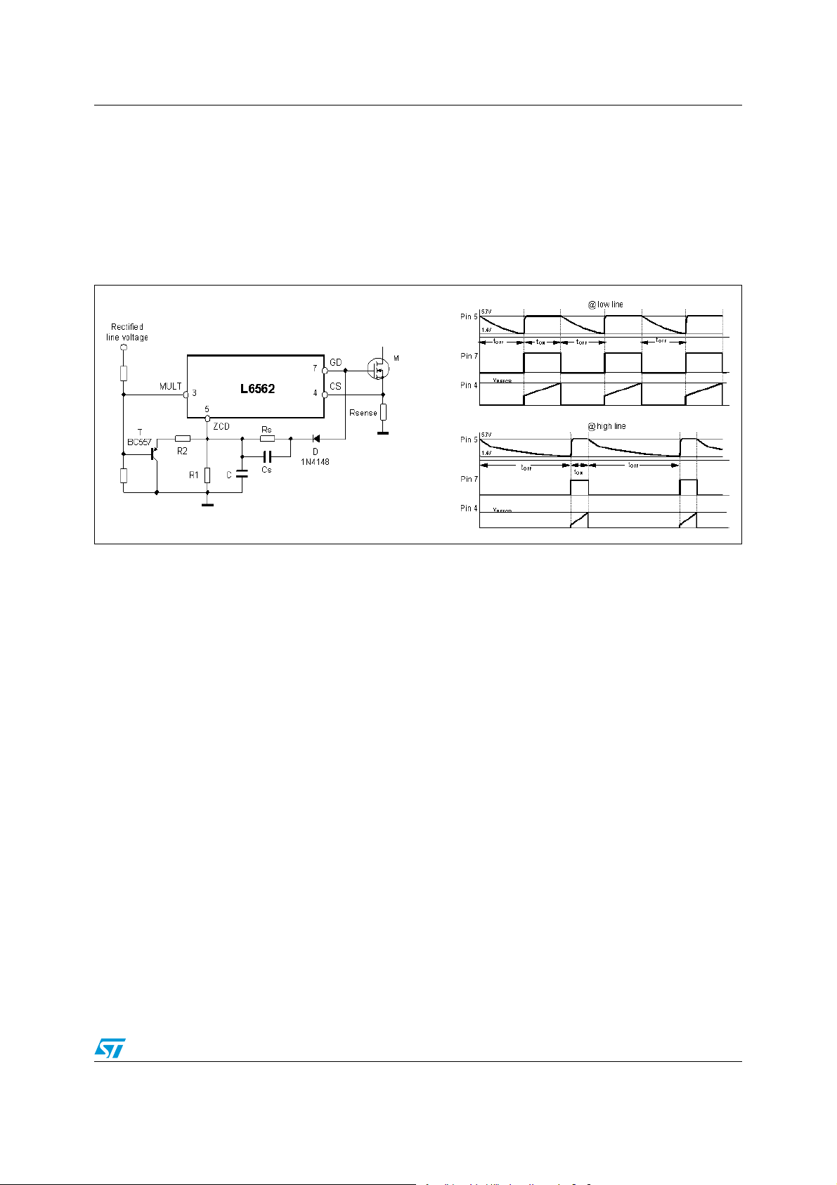
3 Setting up FOT control with the L6562
FOT control is implemented with the L6562 using the circuit shown in Figure 3, which shows
some significant waveforms as well. Before starting the design, the desired value of t
the maximum line voltage must be specified. Application note AN1792 shows that to reduce
high-voltage distortion, t
must be greater than 7µs, hence we choose t
OFF
OFF
= 8µs.
Figure 3. Circuit implementing FOT control with the L6562 and relevant timing waveforms.
OFF
at
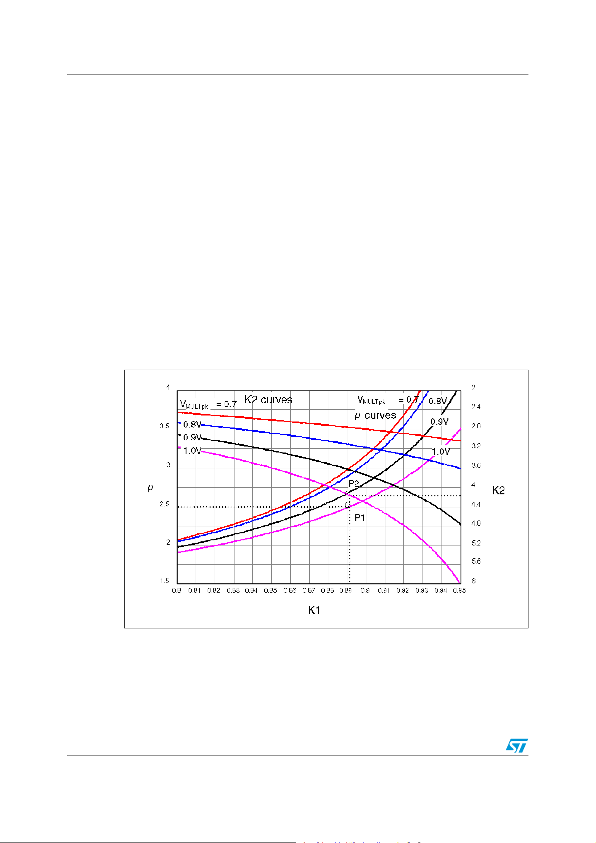
Following the design procedure given in AN1792, with the aid of the diagram of Figure 4:
1. The ratio of the maximum t
2. Consider the value of V
MULTpk
value to the minimum t
OFF
---------------------------- 2.52==
ρ
3.18 10
810
⋅
⋅
6–
6–
at minimum line voltage (V
OFF
MULTpk
value is:
= 1V), in Figure 4 draw
a horizontal line located at ρ = 2.52 (on the left vertical axis) as long as it intercepts the
ρ curve relevant to the value V
=1V in P1. The abscissa of P1 gives the value
MULTpk
K1=0.891.
3. From P1 draw a vertical line as long as it intercepts the K2 curve relevant to V
MULTpk
in P2. The ordinate of P2 (on the right vertical axis) gives the value K2=4.17.
4. The required time constant is:
τ
t
OFFmin
---------------------
K2
3.18 10
---------------------------- 0.76 106–s⋅== =
⋅
4.17
6–
.
5. A capacitor C = 560 pF is selected, then the associated resistance value will be:
R'
τ
0.76 10
--- -
----------------------------- 1357Ω== =
C
560 10
6–
⋅
12–
⋅
.
6. R1 and R2 will be respectively:
R1
R'
---------------- -
1K1–
1357
----------------------- - 12450 Ω== = R2
10.891–
R'
-------
K1
1357
-------------- - 1523Ω== =
0.891
the standard values R1 = 12kΩ and R2 = 1.5kΩ will be chosen.
=1
7/16
Page 8
Setting up FOT control with the L6562 AN1895
7. Assuming that the VCC voltage never falls below 14-15V, the limiting resistor Rs can be
selected according to:
– VF–
V
------------------------------------------------------------------------------------------------------------------------------------------------------------------------- -
Rs
>
I
ZCDx
V
ZCDclamp
--------------------------------------------------------------------------------------------------------------------------------------------------- -+
GDxVZCDclamp
R2 V
ZCDclampVMULTpkmaxVBE
R1R2
––()R1+
where V
5.7V is the clamp value of the ZCD pin voltage, V
diode, I
= 15V is the maximum clamp value of the gate drive voltage, V
GDx
= 10mA the maximum ZCD clamp current D and VBE ≈ 0.55V the emitter-
ZCDx
≈ 0.5V the forward drop on the
F
ZCDclamp
to-base forward drop of T. Substituting:
--------------------------------------------------------------------------------------------------------------------------- -
> 739Ω=
Rs
10 10
3–
5.7 1500 5.7 3– 0.55–()12000⋅+⋅
--------------------------------------------------------------------------------------------- -+⋅
15 5.7– 0.5–
1500 12000⋅
in this case a 1.5kΩ resistor will be chosen
8. Cs will be selected according to the relationship:
V
----------------------------------------------------------------
Cs C
< 560 10
V
ZCDclamp
– VF–
GDxVZCDclamp
12–
⋅ 363p F==
5.7
---------------------------------- -
15 5.7– 0.5–
;
a standard value Cs=330 pF will be used.
Figure 4. Diagrams for the design of the circuit of Figure 3 (valid for wide-range
mains operation).
≈
8/16
Page 9

AN1895 Getting started with the evaluation board
4 Getting started with the evaluation board
The AC voltage, generated by an AC source ranging from 90 to 265 VAC, will be applied to
the input connector, located close to the bottom left-hand corner.
The 400 V
to the load. If an electronic load is going to be used pay attention to the right polarity: the (+)
output terminal is that located closer to the corner.
output is located close to the bottom right-hand corner and will be connected
DC
Warning: Like in any offline circuit, extreme caution must be used
when working with the application board because it contains
dangerous and lethal potentials.
The application must be tested with an isolation transformer
connected between the AC mains and the input of the board
to avoid any risk of electrical shock.
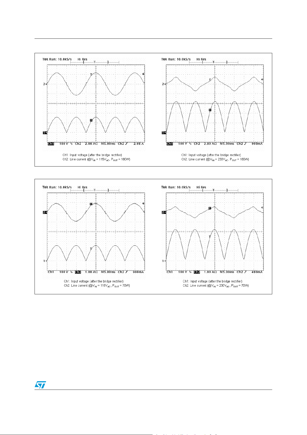
4.1 Testbench results and significant waveforms
The following diagrams summarize the results of certain testbench evaluations. A number of
waveforms under different load and line conditions are shown for user's reference.
Figure 5. Evaluation data
9/16
Page 10

Getting started with the evaluation board AN1895
Figure 6. Compliance with JEIDA-MITI & EN61000-3-2 standards
Figure 7. Harmonic emissions at light load (70W)
Figure 8. Line current waveforms @ P
10/16
OUT
= 375W
Page 11
AN1895 Getting started with the evaluation board
Figure 9. Line current waveforms @ P
Figure 10. Line current waveforms @ P
OUT
OUT
= 180W
= 70W
Note: 1 Note that input LC filter is provided only to clean the line current waveform enough to
prevent the measurement system from being misled by an excessive noise level. The filter is
not designed nor tested for EMI compliance.
2 The board, as is, is able to handle properly an output load as low as 15 W. With lower load
levels, the system will not start up correctly at low line because the OVP generated at startup lasts so long that the V
the system would stop for 600 ms @ V
to levels below 15W may cause the V
voltage drops below the UVLO of the L6562 (e.g. with 4W load
CC
= 90VAC). Load transients from the maximum load
IN
to be lost as well. If supplying the L6562 with an
CC
external source, the minimum load that can be handled properly drops to virtually zero.
11/16
Page 12

References AN1895
5 References
[1] "L6562 Power Factor Corrector" Datasheet.
[2] "Design of Fixed-Off-Time-Controlled PFC Pre-regulators with the L6562", AN1792.
[3] “L6561, Enhanced Transition-Mode Power Factor Corrector”, AN966.
12/16
Page 13

AN1895 Bill of materials
Appendix A Bill of materials
Table 2. Bill of material for EVAL6562-375W evaluation board
R7A, R7B, R7C and R7D 0.68 Ω Metal film, 1W
D1, D2, D3 and D4 1N4148 0.3A / 75V, glass case, Vishay or equivalent
Symbol Value Note
R1A and R1B 120 kΩ
R2A and R2B 620 kΩ
R3 10 kΩ
R4 47 Ω
R5 6.8 kΩ
R6 and R13 6.8 Ω
R8 and R12 1.5 kΩ
R9 12 kΩ
R10A and R10B 499 kΩ
R11 6.34 kΩ
R14 330 Ω
CX1 and CX2 330 nF EPCOS B81131 or equivalent
C1 1 µF 400V, EPCOS B32653 or equivalent
C2 and C4 10 nF
C3 47 µF 25V electrolytic
C5 1 µF
C6 and C10 330 pF
C7 560 pF
C8 470 nF 630V, EPCOS B32653 or equivalent
C9 220 µF 450V, Electrolytic Nichicon LS or equivalent
L1 TOR73 3.9 mH / 6A, supplied by ITACOIL s.r.l.
T1 E4218 Boost inductor. See spec on table 3. Supplied by ITACOIL s.r.l.
BRIDGE KBU8M 8A / 1000V, GI or equivalent
D5 1N5406 3A / 600V, D0201, ON Semiconductor or equivalent
D6 STTH806DTI 8A / 600V, Tandem Hyperfast, TO220, ST
DZ1 1N5248B 18V / 500mW Zener, ON Semiconductor or equivalent
U1 L6562 TM PFC controller, DIP8, ST
M1 and M2 STP12NM50FP 0.3 Ω / 500V, MDmesh
TR1 BC557 PNP, 0.1A / 45V, TO92, On Semiconductor or equivalent
NTC1 BS237 NTC 2.5 Ω, EPCOS or equivalent
F1 --- 8A, 250V
PCB --- FR-4, Cu single layer 35µm, 150 x 81.5 mm
Heat sink OS512 2.12 °C/W, Extrusion Profile, Aavid Thermalloy
TM
, TO220FP, ST
Note: If not otherwise specified, all resistors are 1%, ¼ W, all capacitors are ceramic or plastic
film.
The Bridge, M1, M2 and D6 all share the same heat sink.
13/16
Page 14

Bill of materials AN1895
Table 3. EVAL6562-375W: boost inductor specification (part# E4218, made by ITACOIL s.r.l.)
Core E42/21/7, N67 Material or equivalent
Bobbin Horizontal mounting, 10 pins
Air gap ≈ 1.9 mm for an inductance 1-10 of 550 µH
Windings
Spec &
Build
Pin
Start/End
1/10 Main 20xAWG32 58 (N1) Pins 1 & 2, pins 10 & 9 are shorted on the PCB
6/5 Aux AWG32 6 (N2) Evenly spaced
Winding Wire Turns Notes
14/16
Page 15

AN1895 Revision history
Revision history
Table 4. Document revision history
Date Revision Changes
20-May-2004 2 Initial release.
28-Aug-2006 3 Corrected Equation 1. on page 5. Minor editing changes.
15/16
Page 16

AN1895
Please Read Carefully:
Information in this document is provided solely in connection with ST products. STMicroelectronics NV and its subsidiaries (“ST”) reserve the
right to make changes, corrections, modifications or improvements, to this document, and the products and services described herein at any
time, without notice.
All ST products are sold pursuant to ST’s terms and conditions of sale.
Purchasers are solely responsible for the choice, selection and use of the ST products and services described herein, and ST assumes no
liability whatsoever relating to the choice, selection or use of the ST products and services described herein.
No license, express or implied, by estoppel or otherwise, to any intellectual property rights is granted under this document. If any part of this
document refers to any third party products or services it shall not be deemed a license grant by ST for the use of such third party products
or services, or any intellectual property contained therein or considered as a warranty covering the use in any manner whatsoever of such
third party products or services or any intellectual property contained therein.
UNLESS OTHERWISE SET FORTH IN ST’S TERMS AND CONDITIONS OF SALE ST DISCLAIMS ANY EXPRESS OR IMPLIED
WARRANTY WITH RESPECT TO THE USE AND/OR SALE OF ST PRODUCTS INCLUDING WITHOUT LIMITATION IMPLIED
WARRANTIES OF MERCHANTABILITY, FITNESS FOR A PARTICULAR PURPOSE (AND THEIR EQUIVALENTS UNDER THE LAWS
OF ANY JURISDICTION), OR INFRINGEMENT OF ANY PATENT, COPYRIGHT OR OTHER INTELLECTUAL PROPERTY RIGHT.
UNLESS EXPRESSLY APPROVED IN WRITING BY AN AUTHORIZED ST REPRESENTATIVE, ST PRODUCTS ARE NOT
RECOMMENDED, AUTHORIZED OR WARRANTED FOR USE IN MILITARY, AIR CRAFT, SPACE, LIFE SAVING, OR LIFE SUSTAINING
APPLICATIONS, NOR IN PRODUCTS OR SYSTEMS WHERE FAILURE OR MALFUNCTION MAY RESULT IN PERSONAL INJURY,
DEATH, OR SEVERE PROPERTY OR ENVIRONMENTAL DAMAGE. ST PRODUCTS WHICH ARE NOT SPECIFIED AS "AUTOMOTIVE
GRADE" MAY ONLY BE USED IN AUTOMOTIVE APPLICATIONS AT USER’S OWN RISK.
Resale of ST products with provisions different from the statements and/or technical features set forth in this document shall immediately void
any warranty granted by ST for the ST product or service described herein and shall not create or extend in any manner whatsoever, any
liability of ST.
ST and the ST logo are trademarks or registered trademarks of ST in various countries.
Information in this document supersedes and replaces all information previously supplied.
The ST logo is a registered trademark of STMicroelectronics. All other names are the property of their respective owners.
© 2006 STMicroelectronics - All rights reserved
STMicroelectronics group of companies
Australia - Belgium - Brazil - Canada - China - Czech Republic - Finland - France - Germany - Hong Kong - India - Israel - Italy - Japan -
Malaysia - Malta - Morocco - Singapore - Spain - Sweden - Switzerland - United Kingdom - United States of America
www.st.com
16/16
 Loading...