

Page 1

AN1894
®
- APPLICATION NOTE
VIPower: VI Per 12A NON ISOLATED BUCK AND
BUCK-BOOST CONVERTER REFERENCE BOARD
P. LIDAK - R. HAUSER
ABSTRACT
Presented circuit can be used to produce a single, non isolated positive or negative voltage. It is
dedicated for bu ildi ng an au xiliary pow er sup ply ba sed on the VIPer12A S mo nolithic d evice wi th rath er
low output power required.
1. INTRODUCTION
There are some appli cat io ns, wher e an off- line pow e r supp l y wit hout is o lati on be tween i n put an d out put
can be tolerated a nd rather l ow output current is required. I n this case the converter s hould be sim ple
and low cost. These requirements can be satisfied by a step-down converter based on monolithic device
VIPer12AS that inco rporates the PWM contro ller together w ith the Vertical power MOSFET switch in a
SO8 package. Th e presen ted pow er supply has two var iants. The f irst is a bu ck (ste p-down) co nvert er
with a positive output voltage refer enced to the common grou nd. The second one with negati ve output
voltage is a buck-boost converter. The presented reference board incorporates both variants by different
assembly options.
2. CIRCUIT DESCRIPT ION
2.1 Buck Converter +15V/100mA, +5V/60mA or 20mA (Variant 1)
2.1.1 Operating Cond itio ns
Input Voltage range
Input Voltage Freq uency rang e
Main Output
Second O utput (thr ough linear r egulator)
Total Maximum Output Powe r
2.1.2 Circuit Operation
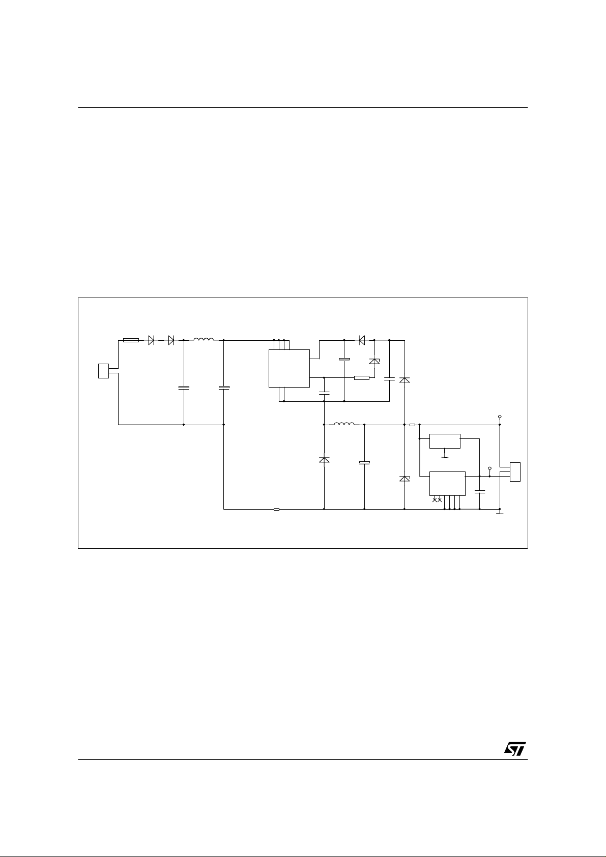
The total schema tic of the power supply can be seen in Figure 1. The output of the conver ter is not
isolated from inpu t. F or t hi s re ason the r efer enc e grou nd is c omm on f or a n inp ut and output conne ct ion
terminal. The inp ut capacitor C1 is charg ed from line via one w ay rectifier co nsisting of diodes D1 and
D2. Two diodes in series are used for EMI reasons to sustain bur st pulses of 2kV. The capacitor C1
together with capacitor C2 and ind uctor L1 for ms an EMI filter. The DC voltage at C2 is then app lied to
the VIPer12 that works as a high side switch . It means the IC and correspon ding supply and feedback
loop circuitry is floating. The IC supply circuit consists of the high voltage diode D4, ceramic capacitor C7
low voltage D7 and capacitor C4. T he voltage feedback loop is provided via z ener diode D3 , resistor R 3
and capacitor C6.
The diode D7 between capacito r C7 and C 4 ensure s the prop er s tart-u p of the conve rter. Thanks to this
diode the feedback loop circu it is separated fr om supply ci rcuit. The internal start-u p current sourc e of
the VIPer12 charges the IC supply capacitor C4 to a specified start-up threshold voltage of about 16V.
March 20 04 1/14
90-264 VAC
50/60 Hz
15V / 100mA
5V / 60 or 20mA
1.6W
Page 2
AN1894 - APPLICATION NOTE
As soon as C4 voltage rea ches th e start- up t hreshold the inter nal 6 0 kHz o scillator se ts the inte rnal flipflop and th rough output driver tur ns-on the inter nal high vo ltage power M OSFET. Th e power M OSFET
applies the bulk capacitor C1 and C2 high voltage to the cathode of the power diode and to one terminal
of the inductor. Since the voltage at the out put capac itor C3 co nnecte d to the induc tor’s second terminal
is much lower than input bulk capacitor voltage the inductor current will ramp-up. As soon as the inductor
current ra mp reache s the VIPer ’s inter nal set -point defi ned b y feedback loop, t he int ernal pow er swi tch
turns off. The inductor keeps the direct ion of the curren t flowing and it reverses th e voltage at C3. The
inductor current then flows through the forward biased D5 diode and charges the output capacitor C3. In
this switch -off phase the sou rce termi nal of the V IPer1 2 sees a negat ive lev el of the forwa rd biase d D5
(when refere nced to ground) so i t can be considered a s grounded. This all ows the inductor cur rent to
flow also through D4 and supply the VIPer12 and give the feedback information about output voltage.
Figur e 1: Schematic diagram of non isolated buck converter with positive output voltage
D1
90...264V~
L
N
clamp
CON1
D2
L1
1.5mH 100mA
C1
+
4.7uF
400V
KMG
BC
8
U1
C4
10uF
4
VDD
Drain15Drain26Drain37Drain4
C2
+
4.7uF
400V
KMG
2
Source11Source2
VIPer12AS
50V
KME
3
FB
R1
10R
GL1M
1000V
1A
GL1M
1000V
1A
3W
L
1
2
N
VDD
C6
22nF
D7
LL4148
+
D3
ZMM13
R3
1k
C7
100nF
D4
RGL34J
600V
0.5A
+15V
CON2
3
+5V
2
C8
100nF
1
clamp
1
Layout Hints: C4, C6 have
to be close to VIPer12A
Assembly options:
(1a): +5V/60mA, +15V/100mA
(1b): +5V/20mA, +15V/100mA
note: all voltages refer to neutral
note: sum of currents is 100mA max.
R6
D6
ZMM18
0R
U3 L78M05CDT (1a)
VIN VOUT
GND
(1b)
U2 L78L05CD
VIN8VOUT
GND36GND47GND23GND12NC25NC1
4
L2
1mH
200mA
D5
RGL34J
600V
0.5A
R5
0R
LBC
C3
+
56uF
35V
LXY
The output voltage of the convert er at the 1 5V term inal is de termin ed by the vo ltage dro p across zener
diode D3 togeth er with voltage dr op across the re sistor R3 and FB pin voltage. Resistor R3 limits the
feedback current to a safe value lower than the maximum rating specified in the data sheet. Capacitor C6
protects the FB input against EMI. One has to take into account the slight variation of the output voltage
with the load. It is because the feedback current reacts to the output load change to adopt switching duty
cycle. The variable feedback current creates different FB voltage, different voltage drop across the
resistor R3 and D3 zener voltage. The feedback current c an change from 0mA (ful l output power) to
about 0.9mA a t no outpu t load. The R3 voltage vari atio n i s 0.9 V a nd F B pi n voltage about 1.2V. The D3
voltage variation depends on the diode V-I characteristics. Diode D6 limits the output voltage at light load
condition and it also protects the U2 voltage re gulator. Regulator U2 a ccommodated in DPAK or SO-8
package is optional and can be assembled if the power supply for a microcontroller or logic part is
required. The DPAK package version of U2 is dedicated for 60mA output current option while U3 in SO-8
can provide max. 20mA.
2/14
Page 3
AN1894 - APPLICATION NOTE
2.1.3 Bill of Materials
The bill of material that corresponds to the Figure 1 can be seen in Table 1.
Table 1: Bill of Material for Non Iso lated Buck Converter with Positive Output Voltage
Ref. Q.ty Value Description
CON1 1 WECO 10.877.002 - clamp, 2 pole, horizontal, type 94 380V 15A
CON2 1 WECO 10.877.003 - clamp, 3 pole, horizontal, type 94 380V 15A
C1, C2 2 4.7uF Nippon Chemi-Con K M G 400 VB 4R7 M Electrolytic capacitor KMG 400V 20%
C3 1 56uF Nippon Chemi-Con LXY 35 VB 56 M F11 Electrolytic capacitor LXY 35V 273mA
0.35R 20 % -
C4 1 10uF Nippon Chemi-Con KM E 50 VB 10 M Electrolytic capacitor KME 50V 20%
C6 1 22nF Ceramic capacitor X7R 50V 10%
C7 1 100nF Ceramic capacitor X7R 50V 10%
C8 1 100nF Ceramic capacitor X7R 50V 10%
D1, D2 2 GL1 M Diotec GL1M d iode, trr=1.5us 1000V 1A
D3 1 ZMM13 Zener diode 13V 0.5W 5%
D4, D5 2 RGL34J Diotec RGL34J Fast recovery diode trr=250ns 600V 0.5A
D6 1 ZMM18 Zener diode 18V 0.5W 5%
D7 1 LL414 8 L L4148 diode 75V 200mA
L1 1 1.5mH EPCOS B78108-S1155-J inductor, bobbin core BC 100mA 23R 10%
L2 1 1mH EPCOS B82144-A2105-J in ductor, large bobbin core LBC 200mA 3.8R 10%
R1 1 10R Yageo 254-0 10R 5% 1J resistor, wirewound, fusible, TK120 CRF 254-4 3W 5%
R3 1 1k resistor, metal film 100V 0.125W 1%
R5 1 0R resistor, metal film
R6 1 0R resistor, metal film
U1 1 VIPer12AS STMicr oelectroni cs VIPer12AS Off-line SMPS Primary IC 730V 0.4A 27R
U2 1 L78L05CD STMicroelectronics L78L05CD positive voltage regulator 5V 100mA 10%, for
variant 1b
U3 1 L78M05CDT STMicr oelectroni cs L78M05CDT positive voltage regulator 5V 0.5A 5%, for
variant 1a
3/14
Page 4
AN1894 - APPLICATION NOTE
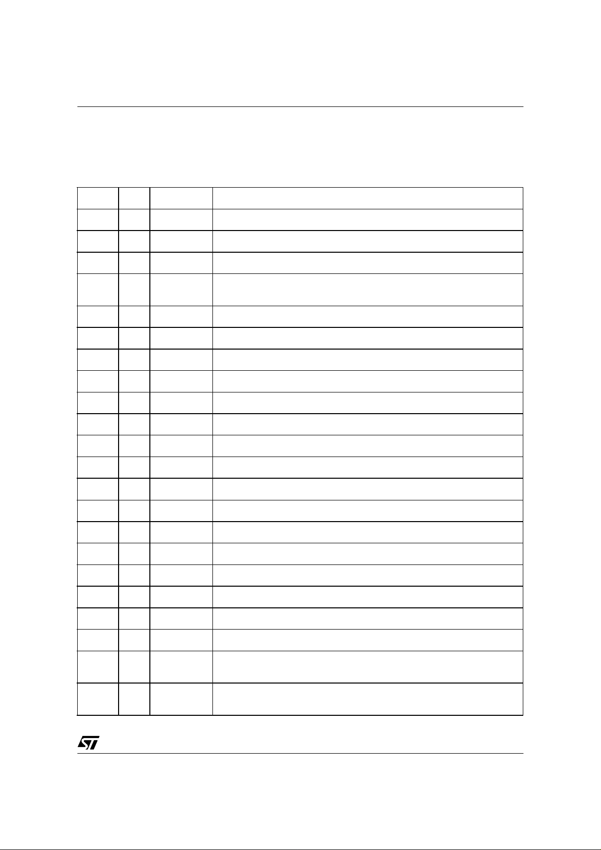
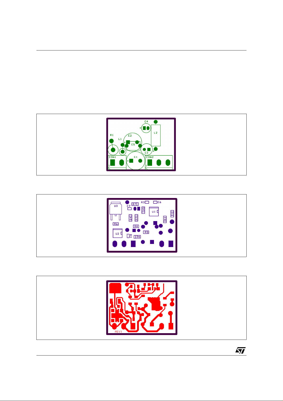
2.1.4 PCB Layout
The PCB is designed as single sided board made of FR-4 material with 35mm copper plating with solder
and silk screen mask. The assembled board co ntains both SMD and through h ole components. The
board incor porates both a buck and buck-boost variant of the converter. The outline dimensions are
38x29mm. Assem bly top side (trough-hole components ) and solder botto m (S MD compon ents) sid e can
be seen in Figure 2 and Figure 3.
Figur e 2: Assembly T op (not in scale)
Figur e 3: Assembly Solder Side (not in scale)
Figur e 4: PCB Layout (not in scale)
4/14
Page 5
AN1894 - APPLICATION NOTE
The PCB layout of the copper connections is depicted in Figure 4. The holes for through-hole
components are not seen in the picture.
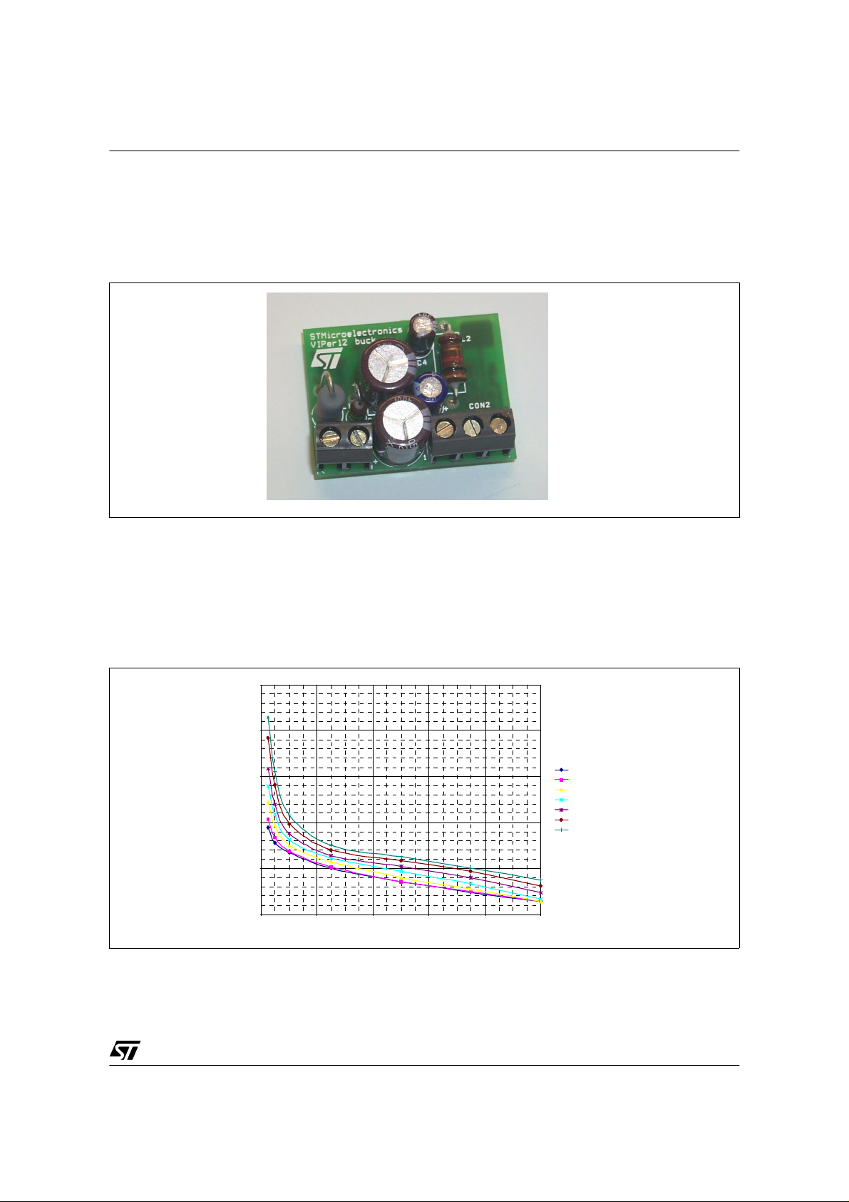
The physical appearance of the converter can be observed from Figure 5.
Figur e 5: Picture of the Converter
2.1.5 Buck Converter Evaluation and Measurements
The output regulation characteristics can be seen in Figure 6. It shows the variation of the output voltage
with output current at specific DC input voltage. The zener diode D6 was not connected during the
measurements
Figur e 6: Output Regulation Characteristics (Parameter is Vin)
19
18
17
16
Output Voltage [V]
15
14
0 0.020.040.060.080.1
Out put Current [A]
125VDC
150VDC
200VDC
250VDC
300VDC
350VDC
375VDC
Using the sam e me asure d v alues, Figure 6 can be redrawn using a different par ameter. Figure 7 shows
the variatio n of the outpu t voltage with inpu t DC voltage change. The output curr ent is the par ameter in
this case.
5/14
Page 6

AN1894 - APPLICATION NOTE
]
Figur e 7: Output Regulation Characteristics (Parameter is I
19
18
17
16
Output Voltage [V]
15
14
125 175 225 2 75 325 375
Input Voltage [V]
out
)
100mA
75mA
50mA
25mA
10mA
5mA
2.5mA
One of the most important and observed characteristics is the converter’s efficiency. Figure 8 depicts the
dependency of the effi cienc y on the inpu t vo ltage (parame ter i s outpu t curren t ) whil e Figur e 9 sh ows the
dependency on the output current (parameter is input voltage).
Figur e 8: Efficiency variation with input voltage (Parameter is I
80
75
70
65
60
E ffi ci en c y [%
55
50
45
40
125 175 225 275 325 375
6/14
Input Voltage [V]
out
)
100mA
75mA
50mA
25mA
10mA
5mA
Page 7

Figur e 9: Efficiency variation with output current (Parameter is Vin)
]
80
75
70
AN1894 - APPLICATION NOTE
65
60
E ffi ci en c y [%
55
50
45
40
0 0.02 0.04 0.06 0.08 0.1
Output Cu rre nt [A]
125VDC
150VDC
200VDC
250VDC
300VDC
350VDC
375VDC
Following pictures starting from Figure 10 to Figure 17 show the most important voltage or current
waveforms at different input and output conditions. Channel 1 (pink) is the power MOSFET Source
terminal voltage of the VIPer12. Channel 4 (red) shows the inductor current. The purpose of those
pictures is to demonstrate the skippi ng cycle function at li ght or no-load condi tion and cycle-by-cycle
primary current limitation at overload or output shorted condition.
Figure 10: Vin=127VDC, I
=100mA Figure 11 : Vin= 127VDC, I
out
= 50mA
out
7/14
Page 8

AN1894 - APPLICATION NOTE
Figur e 12 : Vin= 373VDC, I
= 100mA Figure 13 : Vin= 373VDC, I
out
= 50mA
out
Figur e 14 : Vin= 373VDC, no-load Figure 15: Vin= 127VDC, no-load
Figure 16: Vin= 127VDC, output shorted Figure 17: Vin= 127VDC, output shorted, burst
magnified
8/14
Page 9

AN1894 - APPLICATION NOTE
Furthermore conducted emissions were measured in neutral and line wire using peak or average
detector. The measurements were performed at 230VAC input voltage and the 15V output was fully
loaded by 100mA load. The presented results depicted from Figure 18 to Figure 21 show the results. For
compliance with the EN 55014 standa rd, a small input fil ter ( X-capacitor, commo n mode choke) sho uld
be added, if there is no EMI filter for the complete system. Alternatively, a double sided pcb can be used.
Figure 18: Phase L, average detector Figure 19: Phase L, peak detector
Figure 20: Phase N, average detector Figure 21: Phase N, peak detector
2.2 Inverting Converter -15V/100mA (Variant 2)
2.2.1 Operating Conditions
Input Voltage range
Input Voltage Frequency range
Output
Total Maximum Output Powe r
90-264 VAC
50/60 Hz
-15V / 100mA
1.5W
9/14
Page 10

AN1894 - APPLICATION NOTE
2.2.2 Circuit Operation
The total sc hematic of the power su pply can be seen in Figure 22. The output current flowing to t he
output capacitor C3 is discontinuous for the buck-boost converter (unlike the above described buck
converter). Du ring p ri mar y swit ch ON -time the in ductor curr ent flows through th e indu c tor to gro und a nd
not to the output capacitor as for buck converter. As soon as the primary switch is turned off, the inductor
reverses the voltage between its terminals and current starts to flow through the forward biased D5 diode
and charges the outp ut capacitor C3. In this switc h-off phase the source termina l of the VIPer12 sees
negative level of forward biased D5 and negative output voltage (when referenced to ground). The
converter is called inverting. It i s because the output vo ltage is negative co mpared to the input v oltage
referred to the s ame common ground. B y removin g the jumper R5 an d placeme nt of the ju mper R4 the
buck converter can be easily changed to the inverting buck-boost converter.
Figure 22: Schematic Diagram of Non Isolated Buck-Boost Converter with Negative Output Voltage
D1
90...264V~
CON1
L
N
clamp
D2
L1
R1
10R
GL1M
1000V
1A
GL1M
1000V
1A
3W
L
1
2
N
BC
1.5mH 100mA
C1
+
4.7uF
400V
KMG
8
C2
+
4.7uF
400V
KMG
2
U1
VDD
Drain15Drain26Drain37Drain4
FB
Source11Source2
VIPer12AS
VDD
C4
4
10uF
50V
KME
3
C6
220pF
D7
LL4148
+
D3
ZMM13
R3
1k
C7
100nF
D4
RGL34J
600V
0.5A
R6
Layout Hints: C4, C6 have
to be close to VIPer12A
R4
0R
L2
1mH
200mA
D5
RGL34J
600V
0.5A
LBC
C3
+
56uF
35V
LXY
0R
CON2
3
2
1
clamp
-15V
2.2.3 Buck-Boost Converter Evaluation and Measurements
The output regulation characteristics can be seen in Figure 23. It shows the variation of the output
voltage with output c urrent at specific DC input v oltage. The zener diod e D6 was not connected duri ng
the measurements.
10/14
Page 11

Figure 23: Output Regulation Characteristics (Parameter is Vin)
17
AN1894 - APPLICATION NOTE
16
Output Voltage [V]
15
14
0 0.02 0.04 0.06 0.08 0.1
Output Current [A ]
125VDC
150VDC
200VDC
250VDC
300VDC
350VDC
375VDC
Using the same measured values, Figur e 23 can be redrawn using a different param eter. Figu re 24
shows the variation of the output voltage with input DC voltage change. The output current is the
parameter in this case.
Figure 24: Output Regulation Characteristics (Parameter is I
17
out
)
16
Output Voltage [V]
15
14
125 175 225 275 325 375
Input Voltage [V]
100mA
75mA
50mA
25mA
10mA
5mA
2.5mA
11/14
Page 12

AN1894 - APPLICATION NOTE
]
]
Figure 25 d epicts the dependency of the efficiency on the inp ut voltage (parameter is out put current)
while Figure 26 shows the dependency on the output current (parameter is input voltage).
Figure 25: Efficiency variation with input voltage (Parameter is I
80
75
70
65
60
55
E ffi ci en c y [%
50
45
40
35
125 175 225 275 325 375
I nput Voltage [V]
out
Figure 26: Efficiency variation with output current (Parameter is Vin)
)
10 0m A
75 mA
50 mA
25 mA
10 mA
5mA
12/14
80
75
70
65
60
E ffi ci en c y [%
55
50
45
40
0 0. 02 0.0 4 0.06 0. 0 8 0.1
Output C urrent [A]
125VDC
150VDC
200VDC
250VDC
300VDC
350VDC
375VDC
Page 13

AN1894 - APPLICATION NOTE
Following pictures starting from Figure 27 to Figure 34 show the most important voltage or current
waveforms at d ifferent in put a nd output conditio ns. The ch annel 1 (pink ) is the p ower M OSFET Sour ce
terminal vo ltage of the VIPer12. The channel 4 (red) sho ws the inducto r current. The pur pose of those
pictures is to demonstrate the skippi ng cycle function at li ght or no-load condi tion and cycle-by-cycle
primary current limitation at overload or output shorted condition.
Figure 27: Vin= 127VDC, I
Figure 29: Vin= 373VDC, I
= 100mA Figure 28: Vin= 127VDC, I
out
= 100mA Figure 30: Vin= 373VDC, I
out
= 50mA
out
= 50mA
out
Figure 31: Vin= 373VDC, no-load Figure 32: Vin= 127VDC, no-load
13/14
Page 14

AN1894 - APPLICATION NOTE
Figure 33: Vin= 127VDC, output shorted Figure 34: Vin= 127VDC, output shorted, burst
magnified
Waveforms look very simi lar to th ose p resented f or the b uck con verter. One shou ld notice the neg ative
voltage pres en t o n t he VIP er 12 source after internal swit ch t urn- off. T he lev el of thi s n egati ve vol tage is
equal to the output voltage level.
3. CONCLUSION
A reference board w ith the monol ithic sw itcher V IPer1 2AS was presente d. The way, how the refere nce
board can be easi ly s witc hed between tw o basi c non- iso lated top ol ogies bu c k and buck - boost conv erte r
was described. Depi cted output regulation and over all converter efficiency charact eristics measured at
different working conditions show good performance of this simple VIPer12AS application in such difficult
working environment. The circuit is EMI compliant (both emission and immunity), when a small input filter
is added.
Information furnished is believed to be accurate and r eliable. However, STMicroelect r onics assumes no responsibility for the consequences
of use of such information nor for any infringement of patents or other rights of third parties which may results from its use. No license is
granted by implication or otherwi s e under any patent or patent rights of STMicroel ec tronics. Specificat ions mentioned in this publication are
subject to c hange without notic e. This publicatio n s upersedes and rep lac es all information previously supplied. STMicroelec tronics products
are not authorized for use as critical components in life support devices or systems without express written approval of STMicroelectronics.
Australia - Brazil - Canada - China - Finland - France - Germany - Ho ng K ong - India - Israel - It aly - J apan - Malaysia -
Malta - Moro c c o - S ingapore - Spain - Sweden - Switzerland - Unite d K ingdom - U.S.A.
The ST logo is a trademark of STMicroelectronics
2004 STMicroelectronics - Prin ted in ITALY- All Rights Reserved.
STMicroelectronics GROUP OF COMPANIES
http://www.st.com
14/14
 Loading...