

Page 1

AN1893
Application note
Designing with L6925D, high-efficiency monolithic
synchronous step-down regulator
Introduction
This application note details the main features and application advantages of
STMicroelectronics’ new synchronous step-down regulator. After describing how the device
works and the main features, a step-by-step design section is provided in order to help with
the selection of the external components and the evaluation of the losses. The device
performances are shown in terms of efficiency and thermal results. In conclusion, some
application ideas are proposed.
This new product, realized in BCDV technology, is a high-efficiency monolithic synchronous
step-down regulator capable of delivering up to 800 mA of continuous output current and
regulating the output voltage from 0.6 V up to V
capability. The input voltage ranges from 2.7 V to 5.5 V. The control loop architecture is
based on a constant frequency peak current mode, while high efficiency at light loads is
achieved by a low consumption functionality. The very low quiescent current (25 µA) and
shutdown current (0.2 µA) make the device very suitable to supply battery-powered
equipment (particularly suitable for 1 Li-ion cell) like PDAs and hand-held terminals, DSCs
(digital still cameras) and cellular phones. The switching frequency is internally set at 600
kHz but the device can be externally synchronized up to 1.4 MHz. An internal reference
voltage of 0.6 V (typ), allows the device to regulate minimum output voltage of the same low
value. The low MOSFETs R
interesting features are: hysteretic UVLO, OVP, constant current short-circuit protection,
PGOOD and thermal shutdown. The MSOP8 package allows saving significant board
space.
ensures high efficiency at high output current. Additional
DS(on)
thanks to the 100% duty cycle operation
IN
Figure 1. Application test circuit
February 2009 Rev 3 1/29
www.st.com
Page 2

Contents AN1893
Contents
1 Pin functions . . . . . . . . . . . . . . . . . . . . . . . . . . . . . . . . . . . . . . . . . . . . . . . 5
2 Block diagram . . . . . . . . . . . . . . . . . . . . . . . . . . . . . . . . . . . . . . . . . . . . . . 6
3 Functional description . . . . . . . . . . . . . . . . . . . . . . . . . . . . . . . . . . . . . . . 7
3.1 LBI (low battery input)/LBO (low battery output) . . . . . . . . . . . . . . . . . . . . 7
3.2 UVLO (undervoltage lockout) operation . . . . . . . . . . . . . . . . . . . . . . . . . . . 7
3.3 Modes of operation . . . . . . . . . . . . . . . . . . . . . . . . . . . . . . . . . . . . . . . . . . . 7
3.3.1 Low consumption mode . . . . . . . . . . . . . . . . . . . . . . . . . . . . . . . . . . . . . . 7
3.3.2 Low noise mode . . . . . . . . . . . . . . . . . . . . . . . . . . . . . . . . . . . . . . . . . . . . 8
3.4 System stability . . . . . . . . . . . . . . . . . . . . . . . . . . . . . . . . . . . . . . . . . . . . . 9
3.4.1 Current loop compensation . . . . . . . . . . . . . . . . . . . . . . . . . . . . . . . . . . . 9
3.4.2 Voltage loop compensation . . . . . . . . . . . . . . . . . . . . . . . . . . . . . . . . . . 10
4 Short-circuit protection . . . . . . . . . . . . . . . . . . . . . . . . . . . . . . . . . . . . . 12
4.1 Synchronization . . . . . . . . . . . . . . . . . . . . . . . . . . . . . . . . . . . . . . . . . . . . 13
4.2 DROPOUT operation . . . . . . . . . . . . . . . . . . . . . . . . . . . . . . . . . . . . . . . . 14
4.3 Adjustable output voltage . . . . . . . . . . . . . . . . . . . . . . . . . . . . . . . . . . . . . 14
4.4 OVP (overvoltage protection) . . . . . . . . . . . . . . . . . . . . . . . . . . . . . . . . . . 14
4.5 Hysteretic thermal shutdown . . . . . . . . . . . . . . . . . . . . . . . . . . . . . . . . . . 14
5 Application information . . . . . . . . . . . . . . . . . . . . . . . . . . . . . . . . . . . . . 15
5.1 External component selection . . . . . . . . . . . . . . . . . . . . . . . . . . . . . . . . . 15
5.1.1 Input capacitor . . . . . . . . . . . . . . . . . . . . . . . . . . . . . . . . . . . . . . . . . . . . 15
5.1.2 Output capacitor . . . . . . . . . . . . . . . . . . . . . . . . . . . . . . . . . . . . . . . . . . 15
5.1.3 Inductor . . . . . . . . . . . . . . . . . . . . . . . . . . . . . . . . . . . . . . . . . . . . . . . . . 16
5.1.4 Compensation network (R
5.2 Losses and efficiency . . . . . . . . . . . . . . . . . . . . . . . . . . . . . . . . . . . . . . . . 17
5.2.1 Conduction losses . . . . . . . . . . . . . . . . . . . . . . . . . . . . . . . . . . . . . . . . . 17
5.2.2 Switching losses . . . . . . . . . . . . . . . . . . . . . . . . . . . . . . . . . . . . . . . . . . 18
5.2.3 Gate charge losses . . . . . . . . . . . . . . . . . . . . . . . . . . . . . . . . . . . . . . . . 18
) . . . . . . . . . . . . . . . . . . . . . . . . . . . . . . . 17
1C3
6 Thermal considerations . . . . . . . . . . . . . . . . . . . . . . . . . . . . . . . . . . . . . 19
2/29
Page 3

AN1893 Contents
7 Application board . . . . . . . . . . . . . . . . . . . . . . . . . . . . . . . . . . . . . . . . . . 20
8 Efficiency results . . . . . . . . . . . . . . . . . . . . . . . . . . . . . . . . . . . . . . . . . . . 23
9 Application ideas . . . . . . . . . . . . . . . . . . . . . . . . . . . . . . . . . . . . . . . . . . . 24
9.1 Buck boost topology . . . . . . . . . . . . . . . . . . . . . . . . . . . . . . . . . . . . . . . . . 24
9.2 White LEDs . . . . . . . . . . . . . . . . . . . . . . . . . . . . . . . . . . . . . . . . . . . . . . . 24
9.2.1 Driving white LEDs: buck topology . . . . . . . . . . . . . . . . . . . . . . . . . . . . 25
9.2.2 Driving white LEDs: boost topology . . . . . . . . . . . . . . . . . . . . . . . . . . . . 25
9.2.3 Driving white LEDs: buck-boost topology . . . . . . . . . . . . . . . . . . . . . . . 26
10 Revision history . . . . . . . . . . . . . . . . . . . . . . . . . . . . . . . . . . . . . . . . . . . 28
3/29
Page 4

List of figures AN1893
List of figures
Figure 1. Application test circuit . . . . . . . . . . . . . . . . . . . . . . . . . . . . . . . . . . . . . . . . . . . . . . . . . . . . . . 1
Figure 2. Pin connections . . . . . . . . . . . . . . . . . . . . . . . . . . . . . . . . . . . . . . . . . . . . . . . . . . . . . . . . . . 5
Figure 3. MSOP8 package. . . . . . . . . . . . . . . . . . . . . . . . . . . . . . . . . . . . . . . . . . . . . . . . . . . . . . . . . . 5
Figure 4. Block diagram . . . . . . . . . . . . . . . . . . . . . . . . . . . . . . . . . . . . . . . . . . . . . . . . . . . . . . . . . . . . 6
Figure 5. Low consumption mode . . . . . . . . . . . . . . . . . . . . . . . . . . . . . . . . . . . . . . . . . . . . . . . . . . . . 8
Figure 6. Low noise mode . . . . . . . . . . . . . . . . . . . . . . . . . . . . . . . . . . . . . . . . . . . . . . . . . . . . . . . . . . 8
Figure 7. Slope compensation . . . . . . . . . . . . . . . . . . . . . . . . . . . . . . . . . . . . . . . . . . . . . . . . . . . . . . . 9
Figure 8. Equivalent circuit for the voltage loop analysis . . . . . . . . . . . . . . . . . . . . . . . . . . . . . . . . . . 10
Figure 9. Equivalent circuits during the ON time . . . . . . . . . . . . . . . . . . . . . . . . . . . . . . . . . . . . . . . . 12
Figure 10. Equivalent circuit during the OFF time . . . . . . . . . . . . . . . . . . . . . . . . . . . . . . . . . . . . . . . . 12
Figure 11. Valley current limit protection . . . . . . . . . . . . . . . . . . . . . . . . . . . . . . . . . . . . . . . . . . . . . . . 13
Figure 12. Thermal performance results: V
Figure 13. RDS(on) vs. temperature . . . . . . . . . . . . . . . . . . . . . . . . . . . . . . . . . . . . . . . . . . . . . . . . . . 19
Figure 14. Application board . . . . . . . . . . . . . . . . . . . . . . . . . . . . . . . . . . . . . . . . . . . . . . . . . . . . . . . . 20
Figure 15. Component placement . . . . . . . . . . . . . . . . . . . . . . . . . . . . . . . . . . . . . . . . . . . . . . . . . . . . 20
Figure 16. Top side view . . . . . . . . . . . . . . . . . . . . . . . . . . . . . . . . . . . . . . . . . . . . . . . . . . . . . . . . . . . 20
Figure 17. Bottom side view. . . . . . . . . . . . . . . . . . . . . . . . . . . . . . . . . . . . . . . . . . . . . . . . . . . . . . . . . 21
Figure 18. Schematic demonstration board . . . . . . . . . . . . . . . . . . . . . . . . . . . . . . . . . . . . . . . . . . . . . 21
Figure 19. Low noises vs. low consumption efficiencies . . . . . . . . . . . . . . . . . . . . . . . . . . . . . . . . . . . 22
Figure 20. Efficiency vs. output current . . . . . . . . . . . . . . . . . . . . . . . . . . . . . . . . . . . . . . . . . . . . . . . . 23
Figure 21. Efficiency vs. output current . . . . . . . . . . . . . . . . . . . . . . . . . . . . . . . . . . . . . . . . . . . . . . . . 23
Figure 22. Efficiency vs. output current . . . . . . . . . . . . . . . . . . . . . . . . . . . . . . . . . . . . . . . . . . . . . . . . 23
Figure 23. Positive buck boost application. 1 Li-Ion cell to 3.3 V at 0.25 A . . . . . . . . . . . . . . . . . . . . . 24
Figure 24. Buck topology schematic . . . . . . . . . . . . . . . . . . . . . . . . . . . . . . . . . . . . . . . . . . . . . . . . . . 25
Figure 25. Boost topology schematic . . . . . . . . . . . . . . . . . . . . . . . . . . . . . . . . . . . . . . . . . . . . . . . . . . 25
Figure 26. Buck-boost topology schematic . . . . . . . . . . . . . . . . . . . . . . . . . . . . . . . . . . . . . . . . . . . . . 26
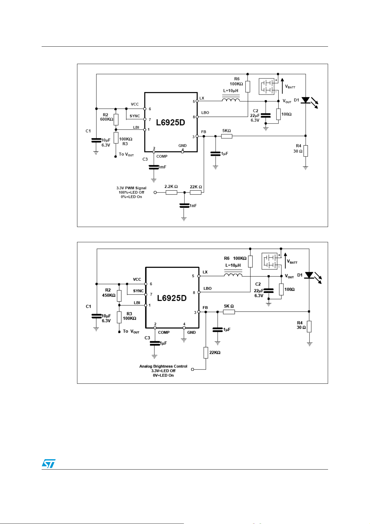
Figure 27. PWM brightness control . . . . . . . . . . . . . . . . . . . . . . . . . . . . . . . . . . . . . . . . . . . . . . . . . . . 27
Figure 28. Analog brightness control . . . . . . . . . . . . . . . . . . . . . . . . . . . . . . . . . . . . . . . . . . . . . . . . . . 27
= 3.7 V V
IN
OUT
= 1.8 V I
= 800 mA . . . . . . . . . . . . . . 19
OUT
4/29
Page 5
AN1893 Pin functions
1 Pin functions
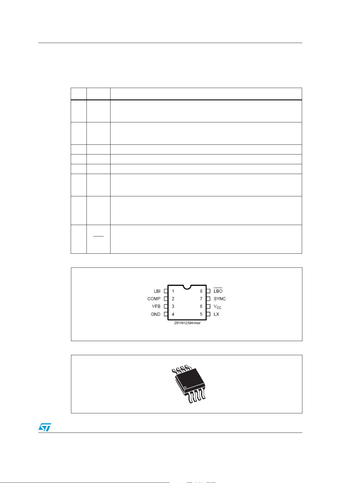
Table 1. Pin description
N. Name Description
Battery low voltage detector input. The internal threshold is set at 0.6 V. The
1 LBI
2 COMP
3 VFB Error amplifier inverting external divider.
4 GND Ground.
5 LX Switches output node. Common point between high side and low side MOSFETs
6
VCC
7 SYNC
8 LBO
external threshold can be adjusted by using an external resistor divider (see
Section 3.1). If not used, the pin can be left floating.
Error amplifier output. A compensation network has to be connected to this pin.
Usually a 220 pF capacitor is enough to guarantee the loop stability (see
Section 3.3.1).
Input voltage. The startup input voltage is 2.8 V (typ) while the operating input
voltage range is from 2.7 V to 5.5 V. An internal UVLO circuit realizes a 200 mV
(typ) hysteresis.
Operating mode selector input. Low consumption mode when connected to a
higher voltage than 1.3 V (up to VCC). Low noise mode when connected to a lower
than 0.5 V (down to GND). Synchronization mode when connected to an external
appropriate clock generator. This pin must not be left floating.
Battery low voltage detector output. If the voltage at the LBI pin drops below the
internal threshold, the LBO pin goes low. The LBO pin is an open drain output. A
pull-up resistor should be connected between the pin and the output voltage. If not
used, the pin can be left floating.
Figure 2. Pin connections
Figure 3. MSOP8 package
5/29
Page 6

Block diagram AN1893
2 Block diagram
Figure 4. Block diagram
6/29
Page 7

AN1893 Functional description
3 Functional description
The main loop uses constant frequency peak current mode architecture. Each cycle, the
high side MOSFET is turned on, triggered by the oscillator, so that the current flowing
through it increases with a slope fixed by the operating conditions. When the sensed current
(a part of the high side current) reaches the output value of the error amplifier E/A, COMP
pin, the internal logic turns off the high side MOSFET and turns on the low side one until the
next clock cycle begins or the current flowing through it goes down to zero (ZERO-
CROSSING comparator). During the load transients, the voltage control loop keeps the
output voltage in regulation changing the COMP pin value, fixing a new turnoff threshold.
Moreover, during these dynamic conditions the choke must not saturate and the inductor
peak current must never exceed the maximum value. This value is in function of the internal
slope compensation (see Section 3.4.1).
3.1 LBI (low battery input)/LBO (low battery output)
A low battery input pin is available. The pin is internally connected to a comparator with a
threshold of 0.6 V. By using an external resistor divider connected between the battery
voltage and the ground it is possible to fix a threshold for the battery voltage. When the
voltage at the LBI pin goes lower than 0.6 V, the LBO pin is forced low. This feature can be
useful for example to have a warning signal when the battery is quite discharged.
3.2 UVLO (undervoltage lockout) operation
The device is particularly designed for equipment powered by a Li-ion battery. These types
of batteries are almost fully discharged when their voltage goes lower than approximately 3
V. For this reason, a UVLO is internally set at 2.8 V, with a hysteresis of 200 mV. Thanks to
this feature, when the battery is fully discharged, the device automatically turns off.
3.3 Modes of operation
3.3.1 Low consumption mode
At light load, the device operates in burst mode in order to keep the efficiency very high also
in these conditions.
While the device is not switching the load discharges the output capacitor and the output
voltage goes down. The COMP pin, due to the feedback loop, increases and when a fixed
internal threshold is reached, the device starts to switch again. In this condition the peak
current limit is set approximately in the range of 200 mA-400 mA, depending on the slope
compensation (see Section 3.4.1). Once the device starts to switch the output capacitor is
recharged. The repetition time of the bursts depend on parameters like input and output
voltages, load, inductor and output capacitors.
Between two bursts, most of the internal circuitries are off, thus reducing the device
consumption down to a typical value of 25 µA. During the burst, the frequency of the pulses
is equal to the internal frequency.
7/29
Page 8
Functional description AN1893
3.3.2 Low noise mode
In case the very low frequencies generated by the low consumption mode are undesirable,
the low noise mode can be selected. The efficiency is a little bit lower compared with the low
consumption mode conditions when working close to zero loads, while the trend is to reach
the efficiency of low consumption mode for intermediate light loads.
The device could skip some cycles in order to keep the output voltage in regulation. In
Figure 5 and 6 the LCM and LNM typical waveforms are shown.
Figure 5. Low consumption mode
Figure 6. Low noise mode
Measurement conditions: V
C
= 22 µF; RC = 40 kΩ; CC = 330 pF
OUT
= 4.2 V; V
IN
= 1.5 V; I
OUT
= 30 mA; L = 6.8 µH; CIN = 10 µF;
OUT
Figure 19 shows a comparison between the efficiency in low noise mode and the efficiency
in low consumption mode.
8/29
Page 9
AN1893 Functional description
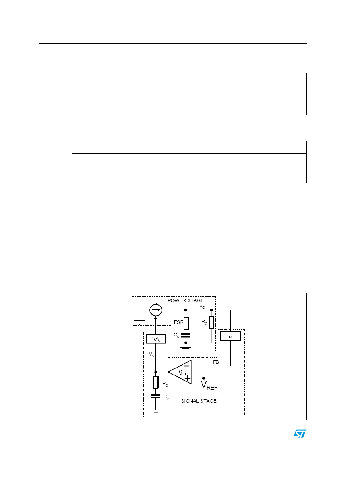
3.4 System stability
Since the device operates with constant frequency peak current mode architecture, the
voltage loop stability is usually not a big issue. For most of the applications a 220 pF
connected between the COMP pin and ground is enough to guarantee the stability. In case
very low ESR capacitors are used for the output filter, such as multilayer ceramic capacitors,
the zero introduced by the capacitor itself can be shifted at a frequency well above the
resonance frequency of the L-C filter and the loop stability could be affected.
Adding a series resistor to the 220 pF capacitor can solve this problem. The right value for
the resistor can be determined by checking the load transient response voltage waveforms.
The current mode stability can be studied in two consecutive steps; first the inner loop is
closed (current loop) and then the second loop stability is considered (voltage loop).
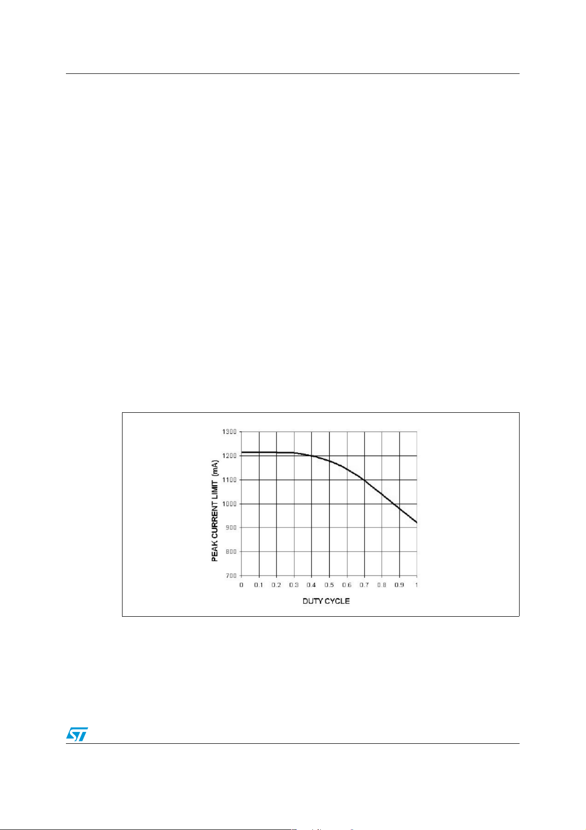
3.4.1 Current loop compensation
The selected control architecture brings many advantages: easy compensation with ceramic
capacitors, fast transient response and intrinsic peak current measurement that simplify the
current limit protection. A known drawback, however, is that the current loop becomes
unstable when the duty cycle exceeds 50%.
This phenomenon is known as "sub-harmonic oscillation" and can be avoided by adding a
slope compensation signal. Due to this fact, the current limit of the device decreases when
the slope compensation signal is applied. The slope compensation is internally implemented
from a duty around 30% and Figure 7 shows how the slope compensation affects the device
current limit.
Figure 7. Slope compensation
The amount of slope compensation depends on the inductor current slope during the OFF
time. This slope, for a given duty cycle, is inversely proportional to the inductor value. Since
the device can be synchronized at a higher frequency, it is reasonable to calculate the
inductor value in terms of it. Finally, the input voltage affects the OFF time slope as well.
This is obvious because, for a given duty cycle, the output voltage (and so the OFF time
inductor current slope) is directly proportional to the input one. In order to better manage
these issues, the amount of slope compensation depends not only on the duty cycle but also
on the switching frequency and the input voltage.
9/29
Page 10
Functional description AN1893
Table 2. Suggested inductor values for different switching frequencies, at V
3.6 V and V
FSW [kHz] Minimum inductor value [∝H]
600 6.8
1000 3.6
1400 2.7
OUT
=1.8 V.
Table 3. Suggested inductor values for different switching frequencies, at
V
= 5 V and V
IN
F
[kHz] Minimum inductor value [µH]
SW
600 8.2
1000 5.6
1400 3.6
OUT
=3.3 V
Ta bl e 2 and 3 indicate the minimum inductor values that ensure the current loop stability
with an input voltage of 3.6 V and 5 V. Also there is a maximum inductor value above which
the loop can become unstable. For example, if the inductor is too high the LC double pole
returns to the bandwidth.
3.4.2 Voltage loop compensation
=
IN
Ideally in a current mode control, after closing the current loop, the pole splitting effect
separates the complex double pole due to the inductor and the output capacitor in 2 different
poles. The pole due to the inductor shifts out of system bandwidth (i.e. the inductor ideally
acts like a current source), while the pole due to the output capacitor remains inside the
bandwidth. Figure 8 shows the equivalent circuit used to study the voltage loop
compensation:
Figure 8. Equivalent circuit for the voltage loop analysis
10/29
Page 11

AN1893 Functional description
In Equation 1 the power stage transfer function is shown:
Equation 1
s()
Hs()
V
O
--------------- -
I
L
sCOESR 1+()R
----------------------------------------------------- -==
s()
sCOESR RO+()1+
O
where R
is the output equivalent resistor load (VO/IO) and ESR is the series resistance of
O
the output capacitors. It can be seen that the pole due to the output capacitor shifts in
frequency based on the load value.
In order to have zero DC error in the voltage regulation, the feedback voltage loop is
implemented with an integrator stage. The transfer function of the signal stage is shown in
Equation 2.
Equation 2
sC
where g
α
g
m
-----------
Gs()
is the integrator transconductance (250 µS). The total gain loop is:
m
A
V
---------------------------- -
⋅=
CRC
sC
1+
C
Equation 3
R
α 1sESRC
+()sCCRC1+()
A
1sCOESR RO+()+()
VsCC
O
where A
(R
/(R2+R3).
2
Ogm
G
LOOP
is the current loop factor (1Ω typ.) and α is the feedback resistor divider ratio
V
s()
--------------------------------------------------------------------------------------------- -=
Once the gain loop is known the system is stabilized with the compensation network as
shown in Section 5.1.4.
11/29
Page 12

Short-circuit protection AN1893
4 Short-circuit protection
The device is provided with two limiting current circuitries, one on the high side and a
second on the low side MOSFET.
Due to the peak current mode architecture, the peak current flowing through the high side
switch is accurately sensed. When this current reaches the peak current limit threshold, the
internal high side MOSFET is turned off. In this way, the ON time, T
output voltage decreases. The minimum T
can be around 200 nsec (T
ON
short-circuit, the peak current could further increase because the intervention of the high
side limiting current is not fast enough. In this case, the valley current limits eliminate the
risks of device failure. To better understand this concept, it's useful to read the below
considerations on the current variation through the inductor during the ON and OFF time.
Equation 4
VINV
–()
∆I
ON
----------------------------------
OUT
⋅=
L
T
ON
(ON time slope)
Equation 5
V
OUT
∆I
OFF
--------------
L
T
⋅=
(OFF time slope)
OFF
, is reduced and the
ON
). In case of
MIN
When V
= 0 V, it can be seen that the inductor current doesn't decrease during the OFF
OUT
time. Therefore the current increases step by step during each cycle. In order to understand
when this phenomenon ends, some real parameters must be considered.
Figure 9. Equivalent circuits during the ON time
Figure 10. Equivalent circuit during the OFF time
12/29
Page 13
AN1893 Short-circuit protection
Considering Figure 9 and 10, in particular during the OFF time, despite the output voltage of
zero, the output current generates on the parasitic resistances the voltage drop necessary
to produce a negative slope. So, the higher the output current is, the higher the negative
slope during the OFF time. In this way, the inductor current finds a stable value. This value
is given by:
Equation 6
I
LIM
----------------------------------------------------------------------------------------------------------------------------------------------------- -=
+()1T
R
NRL
VINT
⋅–()RPRL+()T
MINFSW
⋅()⋅
MINFSW
⋅()⋅+⋅[]
MINFSW
where T
resistance of the low side and high side MOSFETs respectively, R
resistance and R
conditions, the maximum current value depends both on the application conditions (like V
and F
is the minimum ON time, FSW is the switching frequency, RN and RP are the ON
MIN
is the equivalent output resistance. As it can be seen, in these extreme
O
), the inductor parasitic resistor RL, and the MOSFETS R
SW
is the inductor series
L
DS(on) RN
and RP . It does
IN
not depend on the peak current limit at all. In order to limit the output current to a safe value
even in extreme short-circuit conditions, a current limit has also been introduced on the low
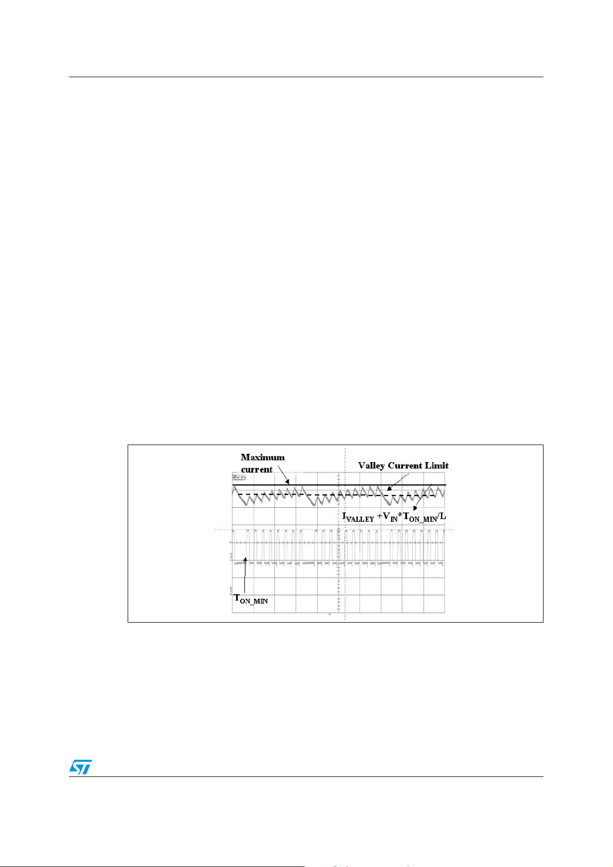
side MOSFET: this operates as a valley current limit, as shown in Figure 11. The high side
MOSFET does not turn on until the inductor current exceeds the valley current limit. This
implies that, depending on the over current conditions, the device skips some cycles, thus
reducing the equivalent switching frequency in order to limit the output current. With this
approach, the maximum peak current is definitively limited to:
Equation 7
VINT
I
LIMIVALLEY
MIN
----------------------+=
L
Figure 11. Valley current limit protection
4.1 Synchronization
The device can be synchronized with an external signal from 500 kHz up to 1.4 MHz through
the internal PLL. When the device is locked, the external signal and the high side turn-on
rising edges are aligned. In this case the low noise mode is automatically selected. The
device eventually skips some cycles in very light load conditions depending also on the
input/output conditions. The internal synchronization circuit is inhibited in short-circuit and
13/29
Page 14

Short-circuit protection AN1893
overvoltage conditions in order to keep the involved protections effective. The
synchronization signal amplitude can range typically from 1 V to V
and the duty factor can
CC
range typically from 20% to 80%. Sometimes, if the synchronization signal duty cycle is very
similar to the application duty factor, noise can be detected on the LX pin. In this case some
practical solutions are:
1. Change the synchronization signal duty factor
2. Decrease the synchronization signal amplitude
3. Add 20 pF capacitor between the Comp pin and ground.
The device switches at 600 kHz (typ.) if no synchronization signal is applied.
4.2 DROPOUT operation
When the input voltage is a Li-Ion battery, the voltage ranges from a minimum of 3 V or less
to 4.1 V - 4.2 V (depending on the anode material). In case the regulated output voltage is
from 2.5 V and 3.3 V, the device can work in linear mode or dropout operation. The minimum
input voltage necessary to ensure output regulation can be calculated as:
Equation 8
V
INMIN
---
VOIOR
DS on()HSMAXRL
+()⋅+=
where R
DS(on)_HS_MAX
is the maximum high side resistance and RL is the series inductor
resistance.
4.3 Adjustable output voltage
The output voltage can be adjusted by an external resistor network from a minimum value of
0.6 V up to the V
. The output voltage value is given by:
IN
Equation 9
V
OUT
Thanks to the very low FB leakage current (typ. 25 nA), high R3, R2 values can be chosen in
hundreds of kΩ increasing the system efficiency also at very low load.
4.4 OVP (overvoltage protection)
The device has an internal output overvoltage protection. If the output voltage goes higher
than 10% of its nominal value, the low side MOSFET is turned on until the output voltage
returns inside the nominal value tolerances. During the overvoltage circuit intervention, the
zero-crossing comparator is disabled so that the device is also able to sink current.
⎛⎞
0.6 1
⋅=
⎝⎠
R
3
------ -+
R
2
4.5 Hysteretic thermal shutdown
The device has also a thermal shutdown protection activated when the junction temperature
rises above 150°C. In this case both the high side MOSFET and the low side one are turned
off. Once the junction temperature falls back to about 95 °C, the device restarts normal
operation.
14/29
Page 15
AN1893 Application information
5 Application information
5.1 External component selection
5.1.1 Input capacitor
The input capacitor must be able to support the maximum input operating voltage and the
maximum RMS input current. Since step-down converters draw current from the input in
pulses, the input current is squared and the height of each pulse is equal to the output
current, neglecting the ripple across the inductor.
The RMS input current (flowing through the input capacitor) is:
Equation 10
I
RMSIO
2D2⋅
D
-------------- -–
η
2
D
------ -+⋅=
2
η
Where η is the expected system efficiency, D is the duty cycle and I
the output DC current.
O
Supposing η =1 this function reaches its maximum value at D = 0.5 and the equivalent RMS
current is equal to I
/2.
O
The maximum and minimum duty cycles are:
Equation 11
V
D
MAX
------------------=
V
INMIN
O
Equation 12
MIN
------------------- -=
V
INMAX
D
V
O
Depending on the output voltage value the worst case can be with the maximum or
minimum input battery voltage. Usually the best choice for the input capacitor is the MLCC
(multi layer ceramic capacitor) thanks to its very small size and very low ESR. Ta bl e 4
provides a list of some MLCC manufacturers.
Table 4. Recommended input capacitors
Manufacturer Series Cap value (µF) Rated voltage (V) ESR at 600 kHz (m.)
PANASONIC ECJ 10 to 22 6.3 10
TAIYO YUDEN JMK 10 to 22 6.3 10
5.1.2 Output capacitor
The output capacitor is very important to satisfy the output voltage ripple requirement. Very
small inductor values reduce size and cost of the application but increase the current ripple.
This ripple, multiplied by the ESR of the output capacitor, is the output voltage ripple.
Tantalum and ceramic capacitors are usually good for this use. Ceramic capacitors have the
lowest ESR for a given size so, for very compact applications they are the best choice.
POSCAP capacitors from Sanyo are also a good choice for the output filter.
15/29
Page 16
Application information AN1893
Ta bl e 5 gives a list of some capacitor manufacturers.
Table 5. Recommended output capacitors
Manufacturer Series Cap value (µF) Rated voltage (V) ESR (m.)
PANASONIC ECJ 10 to 47 6.3 10
PANASONIC EEF 22 to 47 6.3 60 to 90
TAIYO YUDEN JMK 10 to 47 6.3 10
SANYO POSCAP TPA 47 to 100 6.3 80 to 100
5.1.3 Inductor
The inductor value fixes the ripple current flowing through the output capacitor. The ripple
current is usually fixed at 20% - 30% of the output current and is approximately obtained by
the following formula:
Equation 13
–()
V
INVOUT
----------------------------------
L
⋅=
T
I∆
ON
For example, with V
and I
= 600 mA and ∆I = 200 mA, the inductor value is about 6 µH. The peak current
O
= 3.3 V, VIN = 4.2 V (Li-ion battery fully charged), FSW = 600 kHz
OUT
through the inductor is given by:
Equation 14
I
PKIO
I∆
---- -+=
2
It can be seen that if the inductor value decreases, the peak current (that has to be lower
than the current limit of the device) increases. This peak current must be lower than the
saturation current of the choke.
This is particularly important when using ferrite cores because they can hardly saturate (the
inductance value decreases abruptly when the saturation threshold is exceeded thus
causing an abrupt increase of the current flowing through it). The inductor should be
selected also considering the system stability, (see Section 3.4.1). Moreover the inductor
selection should be made, taking into account the inductor parasitic resistance because a
value that is too high can decrease the efficiency. Ta bl e 6 lists some inductor manufacturers.
Table 6. Recommended inductors
Manufacturer Series Inductor value (µH) Saturation current (A)
DO1607C 6.8 to 15 0.72 to 0.96
Coilcraft
DT1608C 6.8 to 15 0.6 to 1
LPO1704 6.8 to 10 0.8 to 0.9
DO1606T 6.8 to 10 1 to 1.1
Panasonic
16/29
ELL6RH 6.2 to 22 0.7 to 1.4
ELL6GM 6.8 to 10 0.93 to 1.1
Page 17

AN1893 Application information
Table 6. Recommended inductors (continued)
Manufacturer Series Inductor value (µH) Saturation current (A)
To ko
D62CB 10 to 22 0.71 to 1.07
D62C 10 to 22 0.63 to 0.99
5.1.4 Compensation network (R1C3)
As shown in Section 3.4 the system stability can be studied with the loop transfer function
given by Equation 3. If the output capacitor is a ceramic type, the zero due to the ESR
generally is out of the system bandwidth, so the stability of the system is ensured by the
cancellation between the pole due to the output capacitor and the equivalent load and the
R
zero. In Equation 15, a simplified gain loop expression, valid around the transition
1C3
frequency f
Equation 15
Supposing C
system bandwidth), and the output voltage equal to 1.8 V, the R
Equation 16
The nearest standard E12 series value is R
The higher the bandwidth is, the faster the transient response but the bandwidth (and so the
R
value) must be lower than fSW/10 to avoid the effect due to the sampling effect poles as
1
mentioned in Section 3.2. The zero due to the compensation network must be at least 5
times lower than the frequency transition, so the C
is given by:
T
G
= 22 µF, the transition frequency at 0 dB equal to 30 kHz (fT is equal to the
2
R
1
LOOP s()
2π fTC
-------------------
gmα
= 47 kΩ .
1
gmR1α
------------------ -=
sC
2
2
48k Ω==
value:
3
value can be calculated as:
1
Equation 17
The nearest standard value is C
ESR zero is in the system bandwidth and it can be used to stabilize the system so the zero
due to the compensation network is useless (the C
5.2 Losses and efficiency
There are losses affecting the efficiency of the application. Some of these losses are related
to the device and others are related to the external components. The most important losses
are explained in the following paragraphs.
5.2.1 Conduction losses
These losses are basically due to the non-negligible resistances of the internal switches and
the external inductor. Usually the current ripple across the inductor is negligible and in order
to estimate the conduction losses of the inductor, the average output current can be
C
3
2π f
= 470 pF. If the output capacitors are tantalum type the
3
17/29
TR1
500pF==
is necessary to the integrator function).
3
5
-------------------
Page 18

Application information AN1893
considered. The conduction losses of the switches depend also on the duty cycle of the
application. The RMS current flowing through the high side MOSFET is (I
RMS current flowing through the low side MOSFET is (I
)2 · (1-D). So, the total conduction
O
)2 · D while the
O
losses are:
Equation 18
P
MOSIO
2
RPD() RN1D–()RL+⋅+⋅()⋅=
where R
respectively and R
and RN are the series resistance of the high side and low side MOSFETs
P
the series resistance of the inductor. The conduction losses due to the
L
ESR of the input and output capacitors are usually negligible, particularly when using
ceramic caps (very low ESR). Anyway, in case of high ESR values for these caps, their
conduction losses are:
Equation 19
P
where ∆I is the current ripple flowing through the choke and D is the duty cycle of the
application. The conduction losses are particularly important at high current because they
depend on its squared value.
5.2.2 Switching losses
The switching losses are due to the turn on and off of the internal high side MOSFET.
Equation 20
where T
are approximately in the range of 15 ns to 20 ns.This loss is important at high frequency.
ON
and T
OFF
2
CIN COUT,
I
O
P
SWITCHINGVINIOFSW
D1D–()⋅()ESR
⋅⋅ ⋅=
I2∆
------- -
⋅+⋅⋅=
CIN
T
ONTOFF
----------------------------------- -
ESR
12
+()
2
COUT
are the turn-on and turnoff times of the internal high side switch. These
5.2.3 Gate charge losses
The gate charge losses derive from switching the gate capacitance of the internal
MOSFETs. The gate capacitances (C
MOSFETs) are charged and discharged with the input voltage at the switching frequency.
Equation 21
P
GATECHARGEVINCHCL
These losses are also directly proportional to the switching frequency and input voltage but
are usually negligible compared with the conduction and switching losses.
18/29
H
-
for the high side MOSFETs and CL for the low side
+()F
⋅⋅=
SW
Page 19

AN1893 Thermal considerations
6 Thermal considerations
Depending on the electrical application conditions (input voltage, switching frequency, and
output current) and ambient temperature, the heat produced by device losses could
increase the junction temperature over its absolute maximum rating. The following relation
can be used to estimate the junction temperature of the device:
Equation 22
TJTAR
where T
is the ambient temperature of the application, R
A
junction to ambient of the package and P
R
equal to 180 °C/W. P
depends a little bit on the application board but it can be considered approximately
TH_JA
is given by:
TOT
Equation 23
P
TOTPMOSPSWITCHINGPGATECHARGE
++=
TOT
⋅+=
THJAPTOT
is the thermal resistance
TH_JA
is the overall power dissipated by the device.
-
Figure 12. Thermal performance results: V
Figure 13. R
vs. temperature
DS(on)
= 3.7 V V
IN
OUT
= 1.8 V I
= 800 mA
OUT
For a better estimation of the power dissipated, it can be useful to consider the MOSFET’s
R
variation with the temperature, as shown in Figure 13.
DS(on)
19/29
Page 20

Application board AN1893
7 Application board
Figure 14. Application board
Demonstration board layout
In the figures below the demonstration board layout is shown.
Figure 15. Component placement
Figure 16. Top side view
20/29
Page 21

AN1893 Application board
Figure 17. Bottom side view
Demonstration board schematic
The very small package and high switching frequency allows a very compact application.
The demonstration board circuit is shown in Figure 18:
Figure 18. Schematic demonstration board
Table 7. Bill of material
Reference Part number Description Manufacturer
C1 ECJ3XBOJ106K 10 µF 6.3 V Panasonic
C2 ECJ4XBOJ226M 22 µF 6.3 V Panasonic
C3 C0406C221J5GAC 220 pF, 5% 50 V Kemet
R1 10 kΩ 1% 0402 Neohm
R2 450 kΩ 1% 0402 Neohm
R3 100 kΩ 1% 0402 Neohm
21/29
Page 22

Application board AN1893
Table 7. Bill of material (continued)
Reference Part number Description Manufacturer
R4 100 kΩ 1% 0402 Neohm
R5 200 kΩ 1% 0402 Neohm
R6 100 kΩ 1% 0402 Neohm
L1 ELL6GM100M 10 µH 0.9 A Panasonic
Figure 19. Low noises vs. low consumption efficiencies
22/29
Page 23

AN1893 Efficiency results
8 Efficiency results
Some efficiency results are shown below in Figure 20, 21, and 22.
Figure 20. Efficiency vs. output current
Figure 21. Efficiency vs. output current
Figure 22. Efficiency vs. output current
23/29
Page 24

Application ideas AN1893
9 Application ideas
9.1 Buck boost topology
In portable applications, the input voltage changes a lot due to the battery discharge profile
that often depends on many parameters like temperature, discharge rate, battery ageing,
etc… Moreover, in particular applications, the output voltage requirements can also change.
This could imply that is not possible to provide the desired regulated output voltage by using
simple buck topology. This problem is often present, for example, in systems using a single
Li-Ion cell, whose voltage profile changes from 4.2 V down to 2.7 V or less. In fact, in these
systems, a 3.3 V output is normally required to power processor I/O, memory and logic.
Adopting buck topology, the 3.3 V output can be regulated until the battery voltage is
approximately 3.4 V, also depending on the minimum dropout of the regulator. Depending
on the battery type and conditions, this would leave unused some 20% - 30% of its capacity.
Another application, even more critical, is the power management of 3G phones, where a
3.7 V or more can be required to power the RF power amplifier (PA).
In order to use the full battery capacity also in these applications, a positive buck_boost
topology can be used. Figure 22 shows how to implement it. This topology can be more
suitable, compared to a standard buck, depending on the battery discharge profile and the
load conditions. In fact, the efficiency loss of the buck-boost topology can be translated into
an equivalent loss in battery capacity. This can then be compared with the gain in battery
capacity due to the fact that it is used over the full voltage range.
Figure 23. Positive buck boost application. 1 Li-Ion cell to 3.3 V at 0.25 A
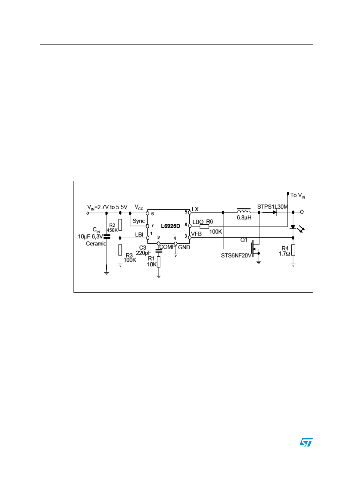
9.2 White LEDs
White LEDs are now widely used both for LCD backlighting and for illumination. Since their
brightness is proportional to the current flowing through them, a current control loop must be
implemented instead of a voltage one. The device can be used in current control
architecture by simply inserting a sense resistor between the FB and GND pins and
connecting the LED in series with it. The loop sets 0.6 V across the sense resistor, and thus,
a constant current flowing through the LED. The current, and by consequence, the
brightness, can be adjusted by changing the resistor value or the voltage across it (by
24/29
Page 25

AN1893 Application ideas
partitioning the FB pin voltage). The forward voltage across a white LED is approximately
3.6 V and so, depending on the input source, appropriate topologies must be used.
9.2.1 Driving white LEDs: buck topology
The simple buck topology can be used when the input voltage source is higher than
approximately 4.5 V which is the case, for example, with the USB bus.
Figure 24. Buck topology schematic
In this case, the maximum device current (800 mA, continuous) can be delivered to the LED.
Moreover, in this topology, the efficiency is maximized.
9.2.2 Driving white LEDs: boost topology
When the input voltage source is always lower than 3 V (which is the case, for example, of 2
cells of a NiMH battery) a boost topology must be implemented, as shown in Figure 25.
Figure 25. Boost topology schematic
25/29
Page 26
Application ideas AN1893
In this case, according to the boost topology, the maximum current that can be delivered
depends on the duty cycle. The relation between the output current and the internal switch
current (assuming a negligible current ripple and 100% efficiency) is given in Equation 24:
Equation 24
I
OUTISWITCH
1D–()=
This topology is possible because the input source is a battery, and so it must not be
referred to ground. A drawback of this approach, intrinsic in the boost topology, is that a path
between the input and output is always present. This does not allow an effective short circuit
protection and can generate a battery discharge also when the device is turned off.
9.2.3 Driving white LEDs: buck-boost topology
In case a single Li-Ion cell is used at the input, a buck-boost topology can be used, as
shown in Figure 26.
Figure 26. Buck-boost topology schematic
The relation from the output current and the switch current is the same as the boost
topology. An advantage of this topology compared with boost topology, is that when the
device is turned off, there is no current path between the input and the output. This allows
an effective short-circuit protection and minimizes the current drawn from the battery when
the device is turned off.
A dimming control can be developed by turning on and off the device with a frequency
around 100-200 Hz in order to avoid LED flickering. Another way to implement the LED
dimming is to reduce the voltage drop across the resistor in series to the LED to a partition
of the FB voltage. Figure 27 and 28 show the relative circuits.
26/29
Page 27
AN1893 Application ideas
Figure 27. PWM brightness control
Figure 28. Analog brightness control
Note: The present application note which is for guidance only, aims at providing customers with
information regarding their products in order for them to save time. As a result,
STMicroelectronics shall not be held liable for any direct, indirect or consequential damages
with respect to any claims arising from the content of such a note and/or the use made by
customers of the information contained herein in connection with their products.
27/29
Page 28

Revision history AN1893
10 Revision history
Table 8. Document revision history
Date Revision Changes
03-Nov-2007 1 Initial release
17-Apr-2008 2
26-Feb-2009 3 Modified: Section 5.1.1
– Document reformatted. No content change
– Changed: Figure 13.
28/29
Page 29

AN1893
Please Read Carefully:
Information in this document is provided solely in connection with ST products. STMicroelectronics NV and its subsidiaries (“ST”) reserve the
right to make changes, corrections, modifications or improvements, to this document, and the products and services described herein at any
time, without notice.
All ST products are sold pursuant to ST’s terms and conditions of sale.
Purchasers are solely responsible for the choice, selection and use of the ST products and services described herein, and ST assumes no
liability whatsoever relating to the choice, selection or use of the ST products and services described herein.
No license, express or implied, by estoppel or otherwise, to any intellectual property rights is granted under this document. If any part of this
document refers to any third party products or services it shall not be deemed a license grant by ST for the use of such third party products
or services, or any intellectual property contained therein or considered as a warranty covering the use in any manner whatsoever of such
third party products or services or any intellectual property contained therein.
UNLESS OTHERWISE SET FORTH IN ST’S TERMS AND CONDITIONS OF SALE ST DISCLAIMS ANY EXPRESS OR IMPLIED
WARRANTY WITH RESPECT TO THE USE AND/OR SALE OF ST PRODUCTS INCLUDING WITHOUT LIMITATION IMPLIED
WARRANTIES OF MERCHANTABILITY, FITNESS FOR A PARTICULAR PURPOSE (AND THEIR EQUIVALENTS UNDER THE LAWS
OF ANY JURISDICTION), OR INFRINGEMENT OF ANY PATENT, COPYRIGHT OR OTHER INTELLECTUAL PROPERTY RIGHT.
UNLESS EXPRESSLY APPROVED IN WRITING BY AN AUTHORIZED ST REPRESENTATIVE, ST PRODUCTS ARE NOT
RECOMMENDED, AUTHORIZED OR WARRANTED FOR USE IN MILITARY, AIR CRAFT, SPACE, LIFE SAVING, OR LIFE SUSTAINING
APPLICATIONS, NOR IN PRODUCTS OR SYSTEMS WHERE FAILURE OR MALFUNCTION MAY RESULT IN PERSONAL INJURY,
DEATH, OR SEVERE PROPERTY OR ENVIRONMENTAL DAMAGE. ST PRODUCTS WHICH ARE NOT SPECIFIED AS "AUTOMOTIVE
GRADE" MAY ONLY BE USED IN AUTOMOTIVE APPLICATIONS AT USER’S OWN RISK.
Resale of ST products with provisions different from the statements and/or technical features set forth in this document shall immediately void
any warranty granted by ST for the ST product or service described herein and shall not create or extend in any manner whatsoever, any
liability of ST.
ST and the ST logo are trademarks or registered trademarks of ST in various countries.
Information in this document supersedes and replaces all information previously supplied.
The ST logo is a registered trademark of STMicroelectronics. All other names are the property of their respective owners.
© 2009 STMicroelectronics - All rights reserved
STMicroelectronics group of companies
Australia - Belgium - Brazil - Canada - China - Czech Republic - Finland - France - Germany - Hong Kong - India - Israel - Italy - Japan -
Malaysia - Malta - Morocco - Singapore - Spain - Sweden - Switzerland - United Kingdom - United States of America
www.st.com
29/29
 Loading...