

Page 1

AN1891
APPLICATION NOTE
APPLICATION IDEAS: DRIVING LEDS USING L497X, L597X,
L692X DC- D C CONVERT ERS FAMILIES
This application note, describes th e m ai n applications and dr i ving m et hods for LEDs. After
this, several appli cat io n ide as usi ng ST D C-DC converters are shown.
1 SUMMARY
1 SUMMARY....................................................................................................................... 1
2 INTRODUCTION..............................................................................................................2
3 DRIVING LEDS ................................................................................................................ 2
4 APPLICATION IDEAS ......................................................................................................4
4.1 DC BUS SUPPLY.................................................................................................... 4
4.1.1 L5970D APPLICATION IDEA.............................................................................5
4.1.2 L4973D APPLICATION IDEA.............................................................................6
4.1.3 L6902D APPLICATION IDEA.............................................................................6
4.2 BATTERY POWERED APPLICATION ...................................................................7
4.2.1 L6920D APPLICATION IDEA.............................................................................7
4.2.2 L6926D BOOST TOPOLOGY APPLICATION IDEA....................... .. ................ .8
4.2.3 L6926D BUCK-BOOST TOPOLOGY APPLICATION IDEA...............................9
4.2.4 L6926D BUCK TOPOLOGY APPLICATION IDEA...................... ................ .. ..10
5 CONCLUSION ...............................................................................................................10
AN1891/0604
REV. 2
1/11
Page 2

AN1891 APPLICATION NOTE
2 INTRODUCTION
LED (Light Emitting Diode) is a Light Emitted p-n junction Diode, under forward bias. If a forward bias is app lied between t he p -n la yers, elect ron s and hol es are meet ing i n the ac tive la yer, and recombine the ms elves, emitting photons. If a reverse bias i s applied, they don't move
in the active layer , and c onse quenti ally , no l ight is emit ted. LEDs gener at e pract ical ly a monochromatic light, with a focused beam of a single wavelength. Therefore, there is not wasted
energy, and no filt ers are re qui red to obt ain dif fere nt color s. The emitt ed radiat ion wavel en gth
depends on the dopants. Due to their construction technology, LEDs are not subjected to
shock, vibrations and heat, and this makes their life very long, measured in order of years
(Typically 100.000 hours with an operating temperature comprised between -40°C and
+85°C). Thanks to all these characteristics, LEDs are widely used in particular color-specific,
power-crucial and high reliability application:
■ Mobile appliances
● Mobile phone screen and keyboard backlight
● PDAs, MP3 players and digital camera backlight
■ Signs and displays
● Advertising signs
● Traffic variable messages signs
■ Automotive applications
● Interior appli cation: lights fo r instrumental panel and dashboard
● Exterior lighti ng stop/turn/tail li ghts
■ Signals
● Traffic signals
● Arrows and pedestrian signals
■ Illumination
● Flashlights
● Architectural and design lighting
● Emergency lighting
● Water features and pools
3 DRIVING LEDS
LEDs are devices where the light intensity (brightness), measured in millicandelas, or in Lumens, is proport ional to t he f orwar d curr ent fl owing through th em. Ther e are t wo main c ate gories of LEDs: the white-blue LEDs, with a typical voltage drop of 3-4V, and the green-redyellow ones, wit h a typical voltag e drop, which is about 2V. It is possible to make another di stinction based on th e forward current:
■ Low current LEDs, fr om 15mA to 50mA, mai nly used in th e portable market for backl ight and
signaling applications.
■ High current LEDs, with forward current between 350mA to 1000mA, typically used in
lighting applicat ions.
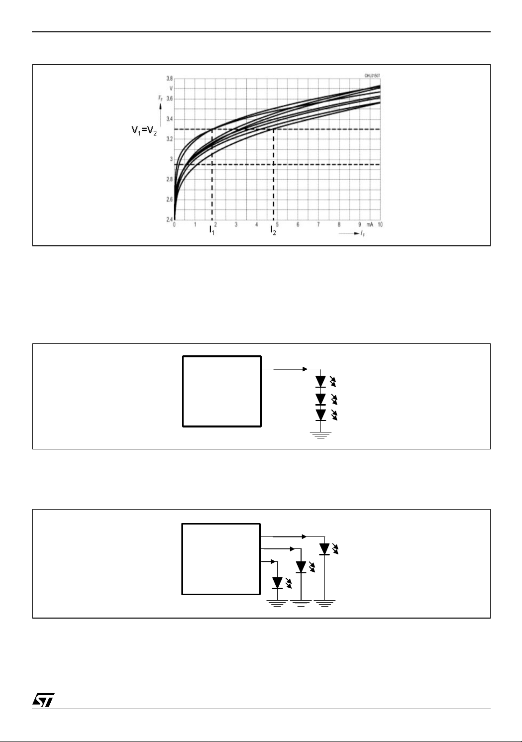
Moreover, applying the same forward voltage to different LEDs of the same type, the current
flowing through them can change significantly. This can be seen in Figure 1, showing the V-I
characteristic of different LEDs of the same type.
2/11
Page 3
AN1891 APPLICATION NOTE
Figure 1. V-I chara cteristic of 8 white LEDs of the same type
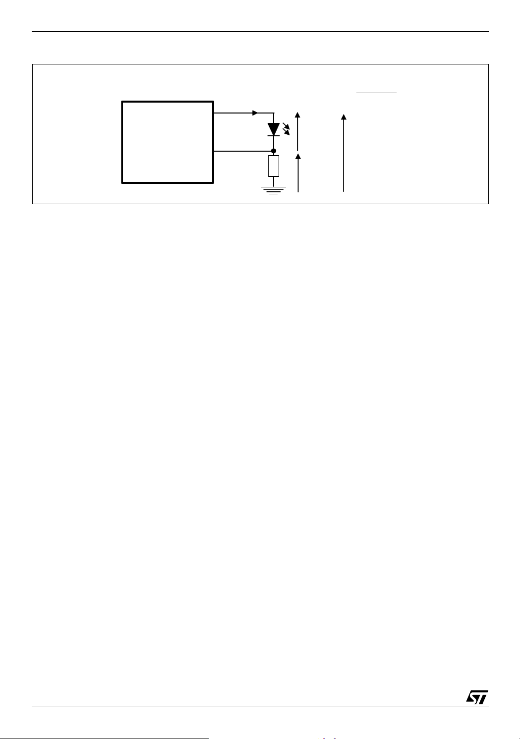
This is why, in order to have a bri ghtness mat ching betwee n differ ent LEDs, the y must be driven by matched constant current sources. Based on these considerations, it is clear that, in
principle, the easiest and cheapest way to drive LEDs is to connect them in series as shown
in Figure 2. However, this implies that the LED driver must provide an output voltage that is
the sum of the LEDs forward volta ge.
Figure 2. Basic schematic of series driven LEDs
I
LED
Constant
Current
Source
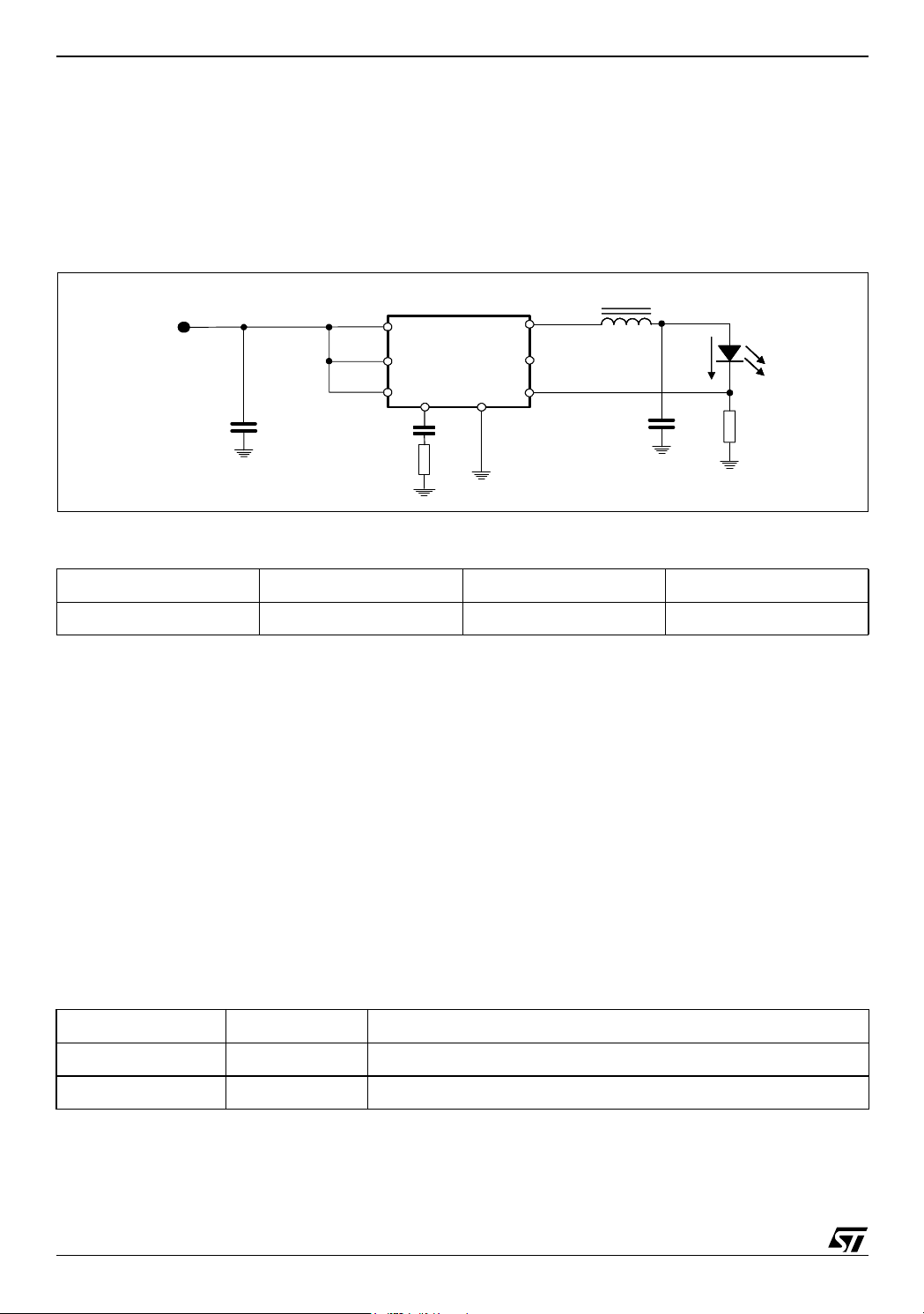
So, in other cases, the preferred solution is to drive LEDs in parallel, matching the different
current sourc es, as shown in Figure 3.
Figure 3. Basic schematic of parallel driven LEDs
I
LED1
Constant
Current
Sources
I
LED3
I
LED2
A typical way to rea li ze a constant current source to drive LEDs is t o use a DC-DC converter,
as shown in Fi gure 4. Since the voltage control loop of the device regulates the voltage at the
FB pin, a constant current source can be obtained simply connecting a resistor between this
pin and GND.
3/11
Page 4
AN1891 APPLICATION NOTE
FB
SENS
Figure 4. Basic schematic of a DC-DC driving LEDs
I
LED
I
LED
=
V
R
E
DC-DC
Driver
FB
R
V
V
OUT
V
The efficiency of the system is given by the general formula:
P
Eff
out
-----------=
P
in
Eq 1
In case of LEDs, the useful power (that is POUT), is the LEDs power, given by:
n
P
LED
V
=
∑
i1=
⋅
LEDiILEDi
Eq 2
So, the efficiency of the system is:
P
--------------=
LED
P
Eq 3
IN
Eff
The power dissipated on the RSENSE resistor is obviously not contributing to the output power and
so it should be minimized. This impl ie s tha t t he FB pin voltage should be as low as possib le.
4 APPLICATION IDEAS
The best device for a particular application can be selected based on its input voltage range,
output current capabil ity , outpu t voltage r ang e, as in standar d DC-DC choi ce. Howev er, some
particularity of the application emphasizes the importance of other parameters. For example,
a very low FB volt age, in or der to minimi ze the p ower di ssipat ion by the sens e resi stor, is ve ry
important. Besi de thi s, the poss ibil ity to change the volta ge acros s th e sense r esist or, in or der
to easily adjust the LEDs brightness, is often required. The following paragraphs show some
LEDs driving solutions, distinguishing two main application classes:
– DC bus supplied applic ati ons
– Battery powered app li cations
4.1 DC BUS SUPPLY
Most of automotive and lig hti ng applications belo ng to this category. The most common in put
voltages are 12V, 18V, 24V and 4 8V. For these applica tions L497 xD, L597xD and t he L6902 D
families of step-down monolithic DC-DC converters are suggested. Table 1, summarizes the
devices charac ter istics (devices are grouped by family and sor ted by output current):
4/11
Page 5

AN1891 APPLICATION NOTE
Table 1. DC-DC converters with DC bus supply
Device
L4976D 1 0.5 to 50 8 to 55 Up to 300 5.1V Vref Minidip/SO16W
L4971D 1.5 3.3 to 50 8 to 55 Up to 300 Minidip/SO16W
L4978D 2 3.3 to 50 8 to 55 Up to 300 Minidip/SO16W
L4973Dx3.3 3.5 0.5 to 50 8 to 55 Up to 300 5.1V Vref DIP18/SO20
L4973Dx5.1 3.5 5.1 to 50 8 to 55 Up to 300 DIP18/SO20
L6902D 1 0.5 to 35 8 to 36 250 Constant current control, 3.3V
L5970D 1 0.5 to 35 4.4 to 36 250 3.3V Vref SO8
L5972D 1.5 1.23 to 35 4.4 to 36 250 SO8
L5973AD 1.5 0.5 to 35 4.4 to 36 500 3.3V Vref HSOP8
L5973D 2 0.5 to 35 4.4 to 36 250 3.3V Vref HSOP8
Iout
(A)
Vout (V) Vin (V) Fsw (KHz)
Additional
Features
Vref
Packages
SO8
4.1.1 L5970D APPLICATION IDEA
The L5970D is a monolithic step-down power switchin g regulator, capable to deli ver up to 1A
of continuous output curre nt. The input voltage range is comprised between 4.4V to 36V. The
feedback voltage is 1.23V, but with a resistor divider connected with the internal reference of
3.3V, is possi ble to re duce the sen se resi stor volt age. This h elps in or der to r educe the was ted
power and to adjust the LEDs brightness.
Figure 5. L5970D driving up to 6 high current white LEDs
VIN
12V to 24V
10µF
25V
220pF
22nF
4.7KΩ
VCC
COMP
L5970D
GND
INH
OUT
VREF
FB
Vref-Vfb
40KΩ
I
=350 mA
LED
15KΩ
R1
Vfb -Vsense
STPS2L25U
R2
Figure 5 shows how to drive 6 LEDs in series.
The V
SENSE
is reduced down to 0.45V, in order to minimize the wasted power. The formula
used to reduce it is:
V
V
SENSE
V
FB
------------------------------------
–=
–()
REFVFB
R
1
R
⋅
15 µH
2
I
LED
330µF
25V
Rsense
Up to
6 LEDs
1.3Ω
Vled
Vsense
=0.45V
Eq 4
The table below shows the ef fi ciency of the applicat ion.
5/11
Page 6

AN1891 APPLICATION NOTE
e
Table 2. Efficiency results of the L5970D driving series LEDs
Efficiency 1 LED 2 LEDs 3 LEDS 4 LEDs 5LEDS 6LEDs
Vin=12V
Iout=350mA 76% 89% 93.5%
Vin=18V
Iout=350mA 83.5% 90% 95% 90%
Vin=24V
Iout=350mA 86.5% 90% 94.5% 97.5%
4.1.2 L4973D APPLICATION IDEA
This application is really closed to the previous one. The substantial different is in the input
voltage, up to 55V. The device can deliver up to 3.5A of continuous output current. Thus, it is
possible to drive more white LEDs connected in series. Figure 6 shown the schematic circuit
of L4973D supplied with a 48V bus. It is driving up t o 12 high current white LEDs. Even in th is
case, the voltage drop across the sense resistor is minimized for efficiency reasons, by the
same trick used for the L5970D.
Figure 6. L4973D driving up to 12 high current white LEDs
16
5.1V
4,5,6
13,14,15
GND
Vref-Vfb
50KΩ
12
Vfb
9
Boot
2.3
Out
R1
220nF
63V
D1
Vfb-Vsense
78KΩ
R2
150µH
Iled
3x100µF
40V
Up to
12
LEDs
Vled
Vin=48V
220nF
63V
20KΩ
2.7nF
470nF
220nF
Osc
SS
7,8
Vcc
1
17
Comp
18
Sync
L4973V3.3
10
11
INH
9.1KΩ
22nF
Iled=350mA
Rsense
1.4Ω
Vsens
0.5V
The efficiency of this application is given by the following table.
Table 3. Efficiency of L4973D driving up to 12 LEDs
Efficiency 8 LEDs 10 LEDs 12 LEDs
Vin=48V
Iout=350mA 95% 96% 98%
4.1.3 L6902D APPLICATION IDEA
The L6902D is a simple and complete step down switching regulator, with adjustable current
limit. This device is a good solution for LEDs lighting applications, thanks to its inner current
loop that allo ws regulating a cons tant current at the output wit h a minimum voltage dro p across
the external sense re si stor ( 100mV). Fi gure 7 shows a sche mati c appli cati on of L6902D, driving up to 6 high current white LEDs. The device works in current limit mode, set to 350mA;
each LED current is 350mA. The losses on RSENSE are only 70mW.
6/11
Page 7

Figure 7. L6902D driving up to 6 high current white LEDs
µ
µ
AN1891 APPLICATION NOTE
VIN
12V-24V
10
25v
100mV
H
22
Vcc
OUT
COMP
22nF
L6902D
F
220pF
5.1K
GND
Vref
CS+
CS-
FB
STPS340U
100 µF
25v
Up to
6 LEDs
R1
R2
The additional benefit of thi s device is that its v oltage loop can be used to pe rform an over vo ltage protection as in dicated in figure 7.
The table 4 indicate s the efficiency values of this application.
Table 4. Efficiency of L6902D driving up to 6 LEDs
Efficiency 1 LED 2 LEDs 3 LEDS 4 LEDs 5LEDS 6LEDs
Vin=12V
Iout=350mA 75% 89%
Vin=18V
Iout=350mA 86% 89% 96.5%
Vin=24V
Iout=350mA 84% 88% 90% 94% 97.5%
4.2 BATTERY POWERED APPLICATION
Battery powered applications are characterized by lower input voltages compared to the applications shown in the previous pages. In these applications, the input voltage changes with
the battery disch arge profile. The battery types for this kind of applications are:
– Li-Ion cell, with the vol tage range comprised between 4.2V and 2.7V or less;
– Ni-MH cell, with the voltage range between 1.5V to 0.9V.
As a consequence, the Buck topology is not the commonest one. Boost or Buck-Boost topologies are often required. We will focus our application examples on L692xD family, including
a step-up converter (L6920D) and step-down converters (L6925D-L6926D) that can be used
in both Boost a nd i n Buck- Boos t top ology. Some appli catio n ideas are s how b elow, in ord er to
explain how to use these devices in LEDs applications, using external references and dimming.
Table 5. DC-DC converters for battery powered applications
Device Iout (A) Vout (V) Vin (V) Fsw (KHz)
L6920D 1 2 to 5.2 0.6 to 5.5 Not fixed 1.23 TSSOP8
L6925D 0.8 0.6 to Vin 2.7 to 5.5 Up to1400 0.6 MSOP8
L6926D 0.8 0.6 to Vin 2 to 5.5 Up to 1400 0.6 MSOP8
Vfb
Additional Features Packages
(V)
4.2.1 L6920D APPLICATION IDEA
The L6920D is a high efficiency Step-up converter. The start up is guaranteed at 1V, but the
operating input voltage can goes down to 0.6V. With a maximum voltage of 5.5V the device
7/11
Page 8

AN1891 APPLICATION NOTE
can be supplied with many battery types: from 1 Li-Ion cell, or 1 to 3 Ni-MH-Alkaline cells. In
figure 8 is shown the typical application schematic of the device. The voltage Feedback is
1.23V. With the resistor divider, connected to the external reference, it is possible to reduce
the sense voltage down to 0.4V, or less, in order to maximize the efficiency. In table 6 are reported the effic iency result of this appl ication.
Figure 8. L6920D with external reference
100nF
LBI
GND
VREF
Lx
7
2 8
6
L6920D
4 5
1
FB
12.5K Ω
R1
Vext -Vfb
VOUT
____
LBO
3
______
SHDN
1µF
L3.3 µH
R2
5K Ω
Vfb-Vsense
External
Reference
3.3V
10µF
D1
R sense
Iout=350mA
1.15 Ω
Table 6. Efficiency of L6920D driving a 350mA LED
Vin (V) 2 2.5 3 3.5 3.7
Eff (%) 88 88 90 86 84
47µF
Vsense=
0.4V
4.2.2 L6926D BOOST TOPOLOGY APPLICATION IDEA
The L6926D is a h igh efficiency monolithic synchr onous Step-down regulator, with a n operating input voltage ran ge comprised bet ween 2V to 5.5V. The feedback voltage is equal to 0. 6V;
this allows low l osse s on the s ense r esist or. T he dev ice can be use d in di ffer ent top ologi es. In
particular when the input voltage is l ower than the typical LED voltage drop, a Boost topology
can be impl emented, as shown i n Figure 9. This topology i s possible only because the supply
is a battery, not referred to Ground. As typical in Boost topology, this configuration doesn't
have an effe cti ve short cir cuit protection. A battery discharge ca n be generated, when the device is turned o ff. The br ightness c ontrol c an be done by usi ng a PWM sign al. Varying t he duty
cycle of the sign al is possible to change the medium curr ent val ue, in order to adju st the brightness. In this case, the maximum intensity is achieved when the duty cycle of the PWM signal
is equal to 0%. The minimum intensit y is when the duty cycle reaches the 100% .
8/11
Page 9

AN1891 APPLICATION NOTE
Figure 9. L6926D in boost topology with digital adjustable brightness control
10µF
6.3V
Sync
Vcc
RUN
7
6
1
L6926D
2
COMP
1µF
4
GND
5
PGOOD
8
3
LX
VFB
1K
L=10 µH
22µF
5K
1µF
6.3V
+
Vbatt
-
100
Iled
350mA
D1
1.7
3.3V PWM Signal
100%=LED Off
0%=LED On
2.2K
22K
1nF
Table 7. L6926D in boost topology with digital adjustable brightness control
Vin (V) 2.1 2.2 2.3 2.4 2.5 2.6 2.7 2.8 2.9 3.0 3.1 3.2 3.3 3.4
Eff (%) 76 79 80 82 83 85 86 86 87 88 89 89 90 91
4.2.3 L6926D BUCK-BOOST TOPOLOGY APPLICATION IDEA
If a single Li -Ion ce ll i s used t o supp ly the device , the Buc k- Boost t opology is usual ly r equir ed.
In fact, the voltage drop across a white LED is comparable with the Li-Ion cell voltage. The
advantage of this application is that the input voltage range can be higher or lower than the
output ones and so the battery can be used over the full load range. Moreover, when the device is turned off, there isn't current flowing from the input to the output. An actual shutdown
and short circuit protection are allowed. The typical application schematic is shown in figure
10.
Figure 10. L6926D in Buck-Boost topology
VIN=2.7V – 4.2V
C1
10uF
6.3V
Ceramic
Sync
Vcc
RUN
7
6
1
330pF
L6926D
2
COMP
4
GND
LX
5
PGOOD
8
VFB
3
4.7uH
STT5NF20V
STPS1L30M
C2
1uF
6.3V
Iled 350mA
1.7Ω
The efficiency of thi s system is reported in the table below:
Table 8. Efficiency of L6926D driving a 350mA LED in Buck-Boost topology
Vin (V) 2.9 3.0 3.1 3.2 3.3 3.4 3.5 3.6 3.7 3.8 3.9 4.0 4.1 4.2
Eff (%) 58 59 60 61 61 62 62 63 63 64 64 64 64 65
9/11
Page 10
AN1891 APPLICATION NOTE
4.2.4 L6926D BUCK TOPOLOGY APPLICATION IDEA
An USB port give s a volt age ra nge be tween 4. 75V t o 5.25V, and pr ovides a maxi mum curr ent
of 500mA. This is a good solution to drive a single high current white LED, in Buck topology.
Infact, the USB voltag e is al ways hi gher t han the o utp ut vol tage r equire d dr ivin g the LED. The
output voltage is given by the sum of the LED drop and the feedback voltage. The Figure 11
shows the applicati on schematic while the Table 9 reports the efficiency results.
Figure 11. L6926D supplied by USB port
Vin=5V
10µF
6.3V
Sync
Vcc
Vcc
RUN
RUN
C3
220pF
R1
10K
7
7
6
6
1
1
L6926D
L6926D
2
2
COMP
4
4
GND
5
5
PGOOD
PGOOD
8
8
3
3
LX
LX
VFB
L=6.8 µH
Iled
350mA
10µF
6.3V
1.7 Ω
Table 9. Efficiency of L6926D driving a 350mA LED in Buck topology
Vin (V) 5 5.5 5.96
Eff (%) 85 84 84
All the battery p owered ap plication i deas shown i n this pa per, are pe rformed wi th a white LED,
which has a voltage drop of approximately 3.3V, and a forward current of 350mA.
5 CONCLUSION
The aim of this pape r is to sho w how monolit hic DC-DC conver ters can b e used to dri ve LEDs.
The right choice between all the ICs belonging to L497xD, L597xD and L692xD families depends on the final application requirements (power source, number of LEDs, additional functions etc...).
This paper shows only few application ideas about LEDs driving: it is possible to find much
more details o n the speci fic IC s in the dedicated Datasheet and Applic ation Not es availabl e on
ST web site.
Table 10. Revision History
Date Revision Description of Changes
March 2004 1 First Issue
June 2004 2 Add. summary, changed any textes, changed style look.
10/11
Page 11

AN1891 APPLICATION NOTE
The present note which is for guidance only, aims at providing customers with information regarding their products in
order for them to save time. As a result, STMicroelectronics shall not be held liable for any direct, indirect or
consequential damages with respect to any claims arising from the content of such a note and/or the use made by
customers of the information contained herein in connection with their products.
Information furnished is believed to be accurate and reliable. However, STMicroelectronics assumes no responsibility for the consequences
of use of such inf orma tio n nor for any i nfr inge ment of pa tent s or oth er ri ght s of thi rd pa rti es wh ich m ay re sul t fr om it s use . No li cense is granted
by implica tio n o r ot he rw is e un d er a ny pa te nt o r pa te nt righ ts of S TM ic ro el ec tro nic s. Sp ec ific at io ns m e nt ion ed in this pu bl ica tion are subject
to change without notice. This publication supersedes and replaces all information previously supplied. STMicroelectronics products are not
authorized for use as critical components in life support devices or systems without express written approval of STMicroelectronics.
The ST logo is a registered trademark of STMicroelectronics.
All other names are the property of their respective owners
© 2004 STMicroelectronics - All rights reserved
Australia - Belgium - Brazil - Canada - China - Czech Republic - Finland - France - Germany - Hong Kong - India - Israel - Italy - Japan -
Malaysia - Malta - Morocco - Singapore - Spain - Sweden - Switzerland - United Kingdom - United States
STMicr oe le ct ron ic s GR O U P OF CO MP A NI ES
www.st.com
11/11
 Loading...