

Page 1

AN1889
Application note
ESBT
STC03DE170HV in 3-phase auxiliary power supply
Introduction
The need to choose a high value of the fly-back voltage is well known to power supply
designers when efficiency and high duty cycle become important requirements. Threephase auxiliary power supplies, starting from a bulk voltage of 750 V, require theoretically
power transistors with a block voltage capability higher than 1200 V. Practical considerations
linked to better efficiency and safe margin may impose to choose devices with even higher
breakdown voltage (i.e. 1500 V, 1700 V). Looking at the power switches currently available,
while power bipolar transistors are strongly limited in switching frequency operation, Power
MOSFETs show a much lower current capability, which may limit their use to low power
applications. Recently available in the market, the ESBTs (Emitter Switched Bipolar
Transistors) represent a valuable and cost effective alternative for all those applications
where high voltage and high switching frequencies are a must.
This application note describes the realization of a 50 W 3-phase auxiliary power supply by
using the STC03DE170HV as main switch for the fly-back converter. Particular attention has
been given to the transformer design as well as to the ESBT driving circuit requirements.
August 2007 Rev 3 1/33
www.st.com
Page 2

Contents AN1889
Contents
1 ESBT: theory and evolution . . . . . . . . . . . . . . . . . . . . . . . . . . . . . . . . . . . 4
2 Application description . . . . . . . . . . . . . . . . . . . . . . . . . . . . . . . . . . . . . . 7
2.1 Pre-design requisite . . . . . . . . . . . . . . . . . . . . . . . . . . . . . . . . . . . . . . . . . . 8
2.2 Fly-back transformer design . . . . . . . . . . . . . . . . . . . . . . . . . . . . . . . . . . . 11
3 Output circuit . . . . . . . . . . . . . . . . . . . . . . . . . . . . . . . . . . . . . . . . . . . . . . 14
4 Clamping circuit . . . . . . . . . . . . . . . . . . . . . . . . . . . . . . . . . . . . . . . . . . . 15
5 ESBT driving circuit . . . . . . . . . . . . . . . . . . . . . . . . . . . . . . . . . . . . . . . . 16
6 Current transformer core selection . . . . . . . . . . . . . . . . . . . . . . . . . . . . 19
7 PWM driver . . . . . . . . . . . . . . . . . . . . . . . . . . . . . . . . . . . . . . . . . . . . . . . . 22
7.1 Primary side regulation . . . . . . . . . . . . . . . . . . . . . . . . . . . . . . . . . . . . . . 22
7.2 Control loop compensation . . . . . . . . . . . . . . . . . . . . . . . . . . . . . . . . . . . . 22
7.3 Switching frequency and max duty cycle setting . . . . . . . . . . . . . . . . . . . 22
7.4 Current sensing and limiting . . . . . . . . . . . . . . . . . . . . . . . . . . . . . . . . . . . 22
7.5 ESBT gate drive . . . . . . . . . . . . . . . . . . . . . . . . . . . . . . . . . . . . . . . . . . . . 23
8 Start-up network . . . . . . . . . . . . . . . . . . . . . . . . . . . . . . . . . . . . . . . . . . . 24
9 Experimental results . . . . . . . . . . . . . . . . . . . . . . . . . . . . . . . . . . . . . . . . 25
10 PCB layout and list of materials . . . . . . . . . . . . . . . . . . . . . . . . . . . . . . 30
11 Revision history . . . . . . . . . . . . . . . . . . . . . . . . . . . . . . . . . . . . . . . . . . . 32
2/33
Page 3

AN1889 List of figures
List of figures
Figure 1. ESBT symbol and equivalent circuit . . . . . . . . . . . . . . . . . . . . . . . . . . . . . . . . . . . . . . . . . . . 4
Figure 2. ESBT switching operation. . . . . . . . . . . . . . . . . . . . . . . . . . . . . . . . . . . . . . . . . . . . . . . . . . . 5
Figure 3. ESBT cross section . . . . . . . . . . . . . . . . . . . . . . . . . . . . . . . . . . . . . . . . . . . . . . . . . . . . . . . 5
Figure 4. SMPS simplified block schematic diagram . . . . . . . . . . . . . . . . . . . . . . . . . . . . . . . . . . . . . . 7
Figure 5. Simplified fly-back schematic diagram . . . . . . . . . . . . . . . . . . . . . . . . . . . . . . . . . . . . . . . . . 8
Figure 6. ESBT driving circuit and relevant waveforms . . . . . . . . . . . . . . . . . . . . . . . . . . . . . . . . . . . 16
Figure 7. ESBT proportional driving circuit . . . . . . . . . . . . . . . . . . . . . . . . . . . . . . . . . . . . . . . . . . . . 17
Figure 8. ESBT proportional waveforms . . . . . . . . . . . . . . . . . . . . . . . . . . . . . . . . . . . . . . . . . . . . . . 18
Figure 9. ESBT current transformer driver. . . . . . . . . . . . . . . . . . . . . . . . . . . . . . . . . . . . . . . . . . . . . 20
Figure 10. ESBT equivalent circuit. . . . . . . . . . . . . . . . . . . . . . . . . . . . . . . . . . . . . . . . . . . . . . . . . . . . 20
Figure 11. ESBT fly-back schematic diagram . . . . . . . . . . . . . . . . . . . . . . . . . . . . . . . . . . . . . . . . . . . 23
Figure 12. Steady state . . . . . . . . . . . . . . . . . . . . . . . . . . . . . . . . . . . . . . . . . . . . . . . . . . . . . . . . . . . . 25
Figure 13. Turn-on behavior . . . . . . . . . . . . . . . . . . . . . . . . . . . . . . . . . . . . . . . . . . . . . . . . . . . . . . . . 25
Figure 14. Turn-off behavior . . . . . . . . . . . . . . . . . . . . . . . . . . . . . . . . . . . . . . . . . . . . . . . . . . . . . . . . 26
Figure 15. Turn-off losses . . . . . . . . . . . . . . . . . . . . . . . . . . . . . . . . . . . . . . . . . . . . . . . . . . . . . . . . . . 26
Figure 16. Steady state . . . . . . . . . . . . . . . . . . . . . . . . . . . . . . . . . . . . . . . . . . . . . . . . . . . . . . . . . . . . 27
Figure 17. Turn-on behavior . . . . . . . . . . . . . . . . . . . . . . . . . . . . . . . . . . . . . . . . . . . . . . . . . . . . . . . . 27
Figure 18. Turn-off behavior . . . . . . . . . . . . . . . . . . . . . . . . . . . . . . . . . . . . . . . . . . . . . . . . . . . . . . . . 28
Figure 19. Turn-off losses . . . . . . . . . . . . . . . . . . . . . . . . . . . . . . . . . . . . . . . . . . . . . . . . . . . . . . . . . . 28
Figure 20. Steady state at minimum voltage . . . . . . . . . . . . . . . . . . . . . . . . . . . . . . . . . . . . . . . . . . . . 29
Figure 21. Steady state at maximum voltage. . . . . . . . . . . . . . . . . . . . . . . . . . . . . . . . . . . . . . . . . . . . 29
Figure 22. PCB layout . . . . . . . . . . . . . . . . . . . . . . . . . . . . . . . . . . . . . . . . . . . . . . . . . . . . . . . . . . . . . 30
3/33
Page 4
ESBT: theory and evolution AN1889
CBG
1 ESBT: theory and evolution
The "emitter switching" concept was widely investigated a few decades ago with the aim of
improving the trade-off between switching and conduction losses mainly in high voltage
applications.
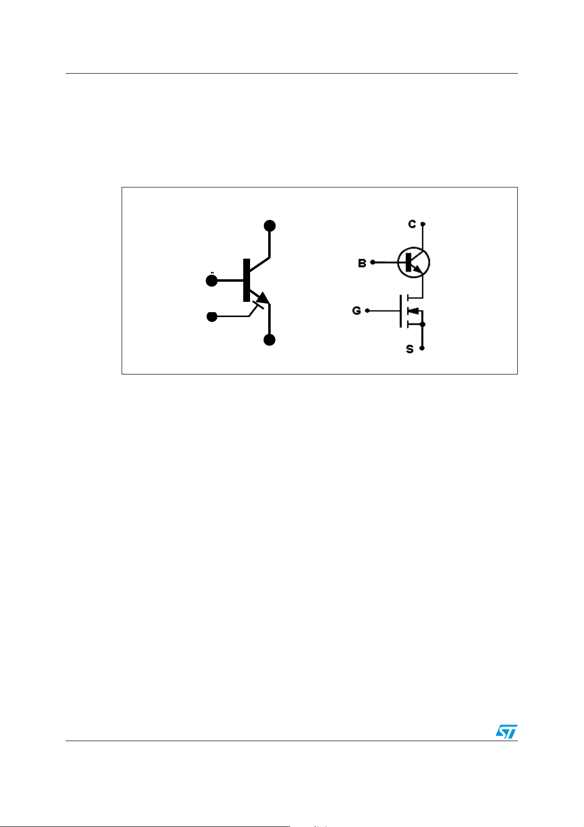
Figure 1. ESBT symbol and equivalent circuit
S
The configuration can be easily implemented by using discrete components and basically
consists in a high voltage Power Bipolar Transistor driven by a low voltage Power MOSFET,
the two devices result connected in cascade configuration, as shown in fig.1. It is clear that
the structure requires two supplying sources: one to ensure the necessary current to the
base of the power bipolar transistor and the second to drive the gate of the Power MOSFET.
Practically, the Power Bipolar Transistor is biased with a constant voltage source between its
base and ground while a PWM controller could directly drive the gate of the Power
MOSFET.
The On condition is guaranteed just by switching on the Power MOSFET. Being the On
voltage drop on the Power MOSFETs negligible compared the V
of the power bipolar
CE(sat)
transistor, we can consider as a first approach the emitter of the power bipolar transistor
grounded.
The driving circuit associated to the base supplies the current needed to saturate the power
bipolar transistor, so that the main conduction losses are those related to the V
CE(sat)
plus
the losses on the input of the power bipolar transistor itself. As a figure of merit, for devices
rated at 1200V we can note that the current density (and consequently in reverse
proportionality the output voltage drop) on Power Bipolar Transistor is 10 times bigger than
that of an equivalent high voltage Power MOSFET.
Starting from the ON-state and switching off the Power MOSFET, the drain current falls
instantaneously down to zero, so that the output current changes its path to the ground
through the base of the transistor itself.
4/33
Page 5
AN1889 ESBT: theory and evolution
V
V
V
V
Figure 2. ESBT switching operation
[V]
GATE
TH
t
[µs]
ESBT equivalent switching-on circuit
[V]
TH
GATE
t [µs]
ESBT equivalent switching-off circuit
Being the negative base current equal to the collector current, the resulting turn-off time is
by far lower than any traditional power bipolar transistor and comparable with that of a high
voltage Power MOSFET. In fact, thanks to the floating emitter configuration, the high value of
the reverse base current results in a fast removal of the charges stored in the base,
achieving both reduced storage time and, most important, the structure results virtually free
of that tail current that characterizes all power bipolar based devices. It is worth to be noted
that the configuration gives an extra safety margin in reverse safe operating area, by
increasing the ruggedness versus the secondary breakdown, in fact since the emitter is
open the phenomenon of crowding current under the emitter finger (with possible creation of
hot spot) is practically absent. Cascade configuration can be implemented in a single four or
five pins package either as hybrid or as a monolithic single chip solution that combines a
vertical NPN Power transistor and a low voltage standard MOSFET. The choice of a suitable
value of thickness and resistivity for the collector drift layer coupled with the most
appropriate edge termination allows in principle to design devices with blocking voltage up
to 3.5 KV. The integration of a low voltage Power MOSFET inside the monolithic structure
had represented the main challenge in designing the ESBT. In particular the power
MOSFET has been integrated inside the emitter region of the Power bipolar stage realizing
a sort of a sandwich structure: thanks to the adopted solution the silicon area depends only
by the BJT size in spite the whole switch is formed by the series connection of the two
devices.
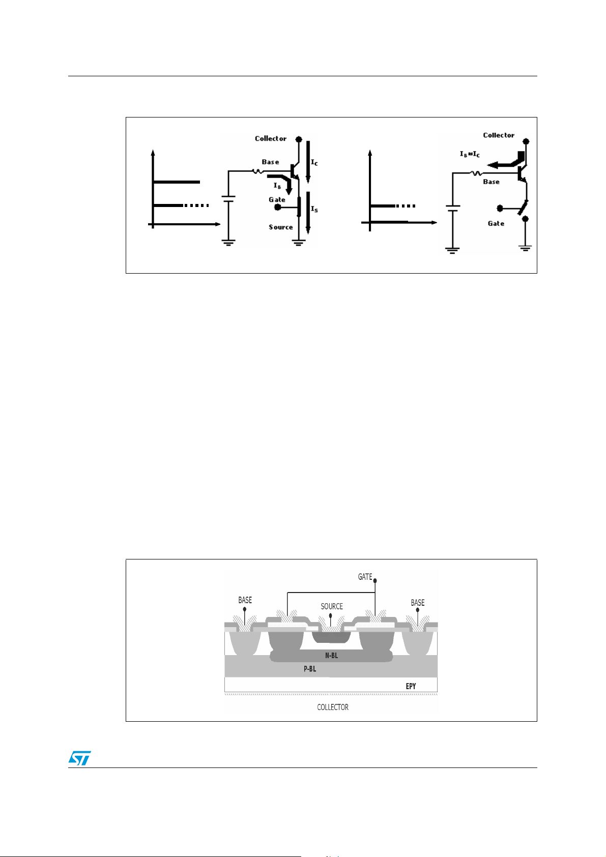
Figure 3. ESBT cross section
5/33
Page 6

ESBT: theory and evolution AN1889
As shown in Figure 3, a DMOS structure is diffused on a higher resistivity layer overlaying
the highly doped emitter region (NBL in the cross section). In terms of diffused and
deposited layers the DMOS structure is quite similar to that of a standard low voltage power
MOSFET even if, of course, its layout is arranged to match the emitter geometry of the BJT
stage. Finally the base contact are placed on a diffused layer deep enough to reach the
base buried layer (PBL).
As previously mentioned to switch-on the ESBT it is necessary to positively bias the gate
with a voltage higher than its threshold (typically 3.5 V for the device in subject), this will
generate, like in all voltage driven transistors, the inversion of the portion of the body region
under the gate oxide of the vertical n-channel MOSFET, so that the emitter results
connected to the ground. In the mean time the base driver supplies the current needed to
saturate the BJT stage leading the ESBT to a high on-state current density due to the high
injection of electrons from the N+ emitter region, similarly to the case of pure power bipolar
transistors. The On-voltage drop is represented by the Collector-Source saturation voltage,
say the V
, and it is consequently given by the contribution of the V
CS(sat)
of the bipolar
CE(sat)
stage plus the small voltage drop of the low voltage MOSFET. Being the bipolar behavior
predominant, the voltage drop results not very sensitive to the temperature variations.
With zero bias in the gate and with grounded base the device behaves like a reverse biased
diode during the off state. The switching-off behavior had already been deeply analyzed at
the beginning of this chapter. It is important to add that the sandwich structure gives an
uniformity of the current density across the whole area of the device. In fact the MOSFET
placed over the BJT (in series with its emitter) acts as a sort of "ideal ballast emitter resistor"
for all of the elementary cells that form the whole transistor. This gives to the device not only
excellent power dissipation but also the suitability to be paralleled with similar devices.
6/33
Page 7
AN1889 Application description
r
2 Application description
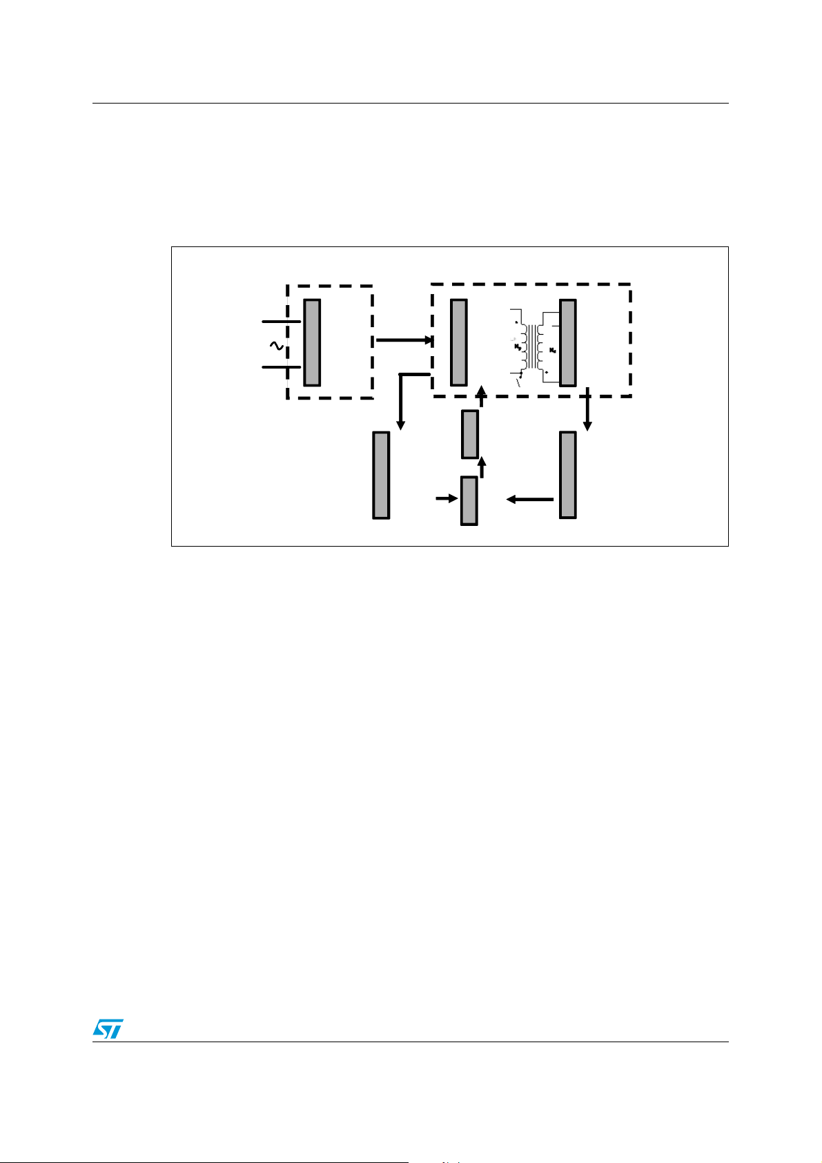
An auxiliary power supply can be schematized in its main functional parts as illustrated in
the simplified block schematic diagram shown in Figure 4.
Figure 4. SMPS simplified block schematic diagram
INPUT
Bridge
+
filter
Feedback
TRANSFORMER + INPUT/OUTPUT
Input
Powe
switch
Input
Driver
CIRCUIT
Output
Output
Feedback
Basically the input voltage is rectified and filtered first, then transferred to the primary side of
the transformer directly through the input circuit of the transformer. This part of the power
supply fixes the voltage clamping at the desired value, the start-up network is also present in
this block to ensure the functionality of the converter during the first pulses. The blocks
power switch and driver, by converting the waveforms from continuous state into alternated
high frequency, allow the transformer, generally operating in discontinuous fly-back mode, to
transfer the stored energy to its secondary side and then to the load through the output
circuit. This basically consists in an ultrafast p-n diode (or Shottky diode) + bulk output
capacitor fixing the maximum acceptable output ripple. When necessary, for a more precise
and lower ripple level, an additional LRC block, working as output post filter network, can be
added.
Power regulation can be achieved through the blocks input feedback (primary regulation) or
output feedback (secondary regulation). By giving to the driver information on the load
requirement, they adapt the input power varying the duty cycle accordingly.
This application note illustrates all design steps needed for the project of a 50W 3-phase flyback converter in discontinuous mode using an ESBT as primary switch.
In this application note the bridge diode + filtering will not be analyzed while the output
circuit will be just mentioned. Most of the attention has been focused on the transformer
design and on the optimization of the driving circuit of the ESBT to allow better performance
in practical applications.
Theoretical results had been validated through a realization of a demo board, its electrical
parameters and component will be shown step by step in the next paragraphs and summed
up at the end of the present note.
7/33
Page 8
Application description AN1889
l
l
ppi
i
g
g
g
g
g
g
2.1 Pre-design requisite
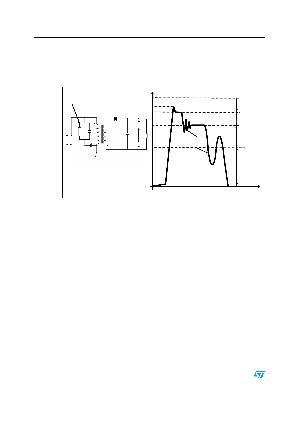
Figure 5 below reported shows the simplified fly-back schematic plus the voltage qualitative
behavior (not in scale) that the switch has to sustain during turn-off operation (point T in the
figure).
Figure 5. Simplified fly-back schematic diagram
Clamping ci rc ui t
Main switch
V
is the maximum input rectified voltage that in 3-phase auxiliary power supplies can be
IN
V
V
r
n
MMaar
iin
OOvveerrvvoollttaaggee
VVoollttaaggee
n
rriin
OOffff
n
iin
V
V
S
S
kkee
V
V
f
f
V
V
IINN
t
t
as high as 750 V.
V
is the reflected fly-back voltage; this is one of the most important parameter in the
fl
transformer design since the input-to-output turn ratio strongly depends on it. The voltage
ringing across V
is generated by the primary inductance that resonates with the equivalent
IN
capacitance at the point T in the figure. This capacitance is mainly due to parasitic
capacitances of the transformer and main switch.
V
is the voltage generated by the leakage inductance of the transformer at primary side.
spike
It must be noted that the energy generated by the mutual inductance at the primary of the
transformer cannot be transferred to the secondary until the leakage inductance is fully
demagnetized. It is the clamping circuit that fixes the value of the voltage at which the
demagnetization process occurs. The voltage ringing in the figure across V
the leakage inductance that resonates with the equivalent capacitance at point T mentioned
before.
The highest overvoltage peak is due to the delay of the diode in the clamping circuit. A good
safety margin must take care of this overvoltage and some transient spikes at start-up.
Transformer design is the major part in a power supply project. A few degrees of freedom
are available to the designer starting from the target data, and most of them are linked each
other so that the final project is often achieved through a re-iteration process.
The table below lists the converter specification data and the first parameters that a
designer has to fix from scratch when a new project of a fly-back converter is going to be
approached. In the last column the values chosen for the present board are reported.
8/33
is generated by
fl
Page 9

AN1889 Application description
Table 1. Converter specification data and fixed parameters
Symbol Description Values
V
V
inmin
V
V
out
AUX
P
out
in
Rectified minimum Input voltage 250
Rectified maximum Input voltage 750
Output voltage 24
Auxiliary output voltage 15
Maximum output power 48
η Converter efficiency 80%
F Switching frequency 50 kHz
V
flyback
V
spike
Reflected fly back voltage 500 V
Max over voltage limited by clamping circuit 200 V
The first choice to be made is the transformer turn ratio NP / NS, where NP and NS are
respectively the number of primary and secondary windings. The calculation of turn ratio is
correlated to the maximum voltage rating of the transistor to be used as primary switch. In
fact looking at the below formula for fly-back operation, the voltage at the point T in Figure 5
is given by:
Equation 1
N
P
VTV
dcmax
-------
N
V0V
S
+()V
Fdiode,
Spike
minarg+++=
obviously
Equation 2
N
P
where V
-------
+()V
V
0VFdiode,
N
S
= the over voltage limited by the clamping circuit.
spike
= the fly-back voltage
=
1
Must be chosen from the designer taking care that the total voltage at point T in Figure 5
does not exceed the maximum breakdown voltage of the device chosen as power switch
according to the Equation 1.
Once fixed the V
, the choice of the designer is limited to fix the fly-back voltage taking
spike
into account the voltage capabilities offered by the standard transistors available. It is worth
noticing that the higher the fly-back voltage the higher the max duty cycle acceptable: higher
duty cycle at fixed output power, leads to lower IRMS with a consequent overall better
efficiency at primary side and an easier design of wide input range converter.
In this case the use of ESBT, having devices with breakdown voltage capability as high as
1700 V can help in that. For the realized demo board with STC03DE170HV we can fix:
● Margin=250 V
● V
while V
=200 V
Spike
, diode being lower than 1 V can be neglected, so that Vfl results being 500 V. From
F
Equation 1 we can now easily calculate the transformer turn ratio:
9/33
Page 10

Application description AN1889
p
Equation 3
BV V
N
-------
N
P
S
– V
---------------------------------------------------------------------------------- -
dcmax
V
0VFdiode,
– minarg–
Spike
+
1700 750– 200– 250–
------------------------------------------------------------ -
24 1+
20===
The second step is to ensure that the converter operates in discontinuous mode, the below
formula will guarantee that the energy on the primary coil will be completely transferred to
the secondary before the next cycle occurs:
Equation 4
N
P
•
V
dcminTonmax
-------
N
V0V
S
+()T
F diode,
resetVflTreset
•==
The next formula, giving a safe margin, guarantees the complete demagnetization of the
primary side.
Equation 5
T
onmaxTreset
=+
0.8T
S
Where T
transformer inductance and T
Combining Equation 4 and Equation 5 T
is the maximum on time, T
onmax
is the time needed to demagnetize the
is the switching time.
S
reset
results being:
onmax
Equation 6
Vfl0.8T
T
onmax
------------------------------ -
V
S
+
dcminVfl
10.66µs≅=
The next step is to calculate the peak current. Fixed the output power to 48 W and the
desiderated efficiency (80% in this case), we have also the freedom to choose the switching
frequency. At this purpose, 50 kHz has been selected. The first step is to calculate the
primary inductance. By using an approximated formula that does not take into account the
losses on the power switch, on the input bridge and on the rectified network, we have:
Equation 7
1
-- -
2
P
1.25P
IN
OUT
-----------------------
2
1
S
pIp
-- -
2
---------------------------------------------------- -===
•
L
T
V
dcmin
2
•
TS•
L
T
onmax
2
hence
Equation 8
2
V
dcmin
L
------------------------------------------------ -= 2.95m H=
P
2.5T
•
SPOUT
T
onmax
2
From here now we can calculate the peak current on primary
Equation 9
V
-------------------------------------------
I
P
It is important also to determine the maximum value of I
of the primary turns as shown in the next section.
10/33
•
dcminTonmax
L
P
0.9A==
primary current to fix the number
rms
Page 11

AN1889 Application description
Equation 10
I
T
P
onmax
I
ms primary()
-------
------------------ - 0.38A==
T
3
S
2.2 Fly-back transformer design
Once defined the turn ratio, the needed primary inductance and the peak current, to
complete the design of the transformer we still need to determine the magnetic core
material, its geometry, and the exact number of primary turns. The choice of correct size
and material of transformer is often an iterative process that may require several try and
error steps before finding the optimal choice. Standard soft ferrite with gaped core and Etype geometry is a common choice for fly-back operation. The calculation of the product of
the areas AP (cross sectional active area of the core multiplied by window area available for
winding) shown in the formula below can help find the dimension of the core:
Equation 11
LPI
3
ms primary()
AP10
------------------------------------ -
1
-- -
2
∆T
KuB
Where ∆T is the maximum temperature variation with respect to the ambient temperature,
KU is the utilization factor of the window (say the portion of the window used for winding that
generally ranges between 0.4 and 0.7), and B
max
By the way all ferrite manufacturers report tables with the suggested core type and size for
given output power and frequency.
1.316
cm4][=
max
is the maximum flux in the core.
For our project the type ED2924-PC40 ferrite material from TDK has been chosen. Next
step is to determine the air gap length (l
(A
) needed to calculate the exact number of primary turns.
L
) of the core and the inductance of a single turn
g
The core must not saturate even at high temperature and in overload conditions (like startup or secondary short circuit), the level of this current in the present project can reach 1.6 A.
By imposing the I
=1.8 A for safety margin, ferrite's manufacturer supplies the
DCmax
following values for the selected ED2924-PC40 core:
● l
= 0.8 [mm]
g
● A
By knowing A
= 0.13 [mH]
L
, the exact number of both primary and secondary turns can be easily
L
calculated.
In fact, being the primary inductance:
Equation 12
LPN2ALNP150=⇒=
Finally from
The closest higher integer has been chosen for the demo board: N
Equation 3: N
=7.5
S
=8
S
At this point we can also calculate the auxiliary winding needed to supply the driver. In our
case the driver used is the UC3842 that from its specification can be driven with 15 V. By
applying again formula1 we can calculate the primary-to-auxiliary turn ratio:
11/33
Page 12

Application description AN1889
Equation 13
N
P
------------ -
N
Aux
V
+
AuxVF diode,
fl
------------------------------------------ -
V
500
--------------- -
15 1+
31 N
Aux
5=⇒===
Before carrying on with the wire dimension calculation, we can preliminary verify if the
selected core is acceptable from a thermal point of view during its normal operation.
Through the Ampere's law we can calculate the B field in normal operation:
Equation 14
B
B
-----
-------
+=+=
l
l
g
µ
0
fe
µ
fe
Being µ
N
pIp
the magnetic permeability in the iron much higher than mo (the magnetic
fe
Hdl HiliHglgHfel
=
=
∫
°
∑
fe
permeability in the air) we can neglect the last item in the Equation 14:
Equation 15
B
PIP
-----
B 170 mT=⇒=
l
g
µ
0
o
C/W, knowing that
N
From the ferrite datasheet the power dissipation is 150 mW/cm3, knowing that the total
volume of the core is about 5 cm
P
= 750 mW.
fe
3
the total power dissipation in the core is about
The thermal resistance of the selected core is 24
Equation 16
∆T
--------
P
fe
∆T18° C=⇒=
R
th
This value allows the designers to operate in safe condition since we have to add also the
losses due to the winding with a further consequent increase in temperature.
The next step is the wire dimension calculation, from both primary and secondary side. First
we must assume the maximum losses on the copper. Normal practice is to choose a
dissipation level comparable with the one achieved in the core, practically we can chose 1W.
From the Joule's law we can calculate the resistance of both primary and secondary
winding.
Equation 17
P
CU
----------------------
R
P
2
2I
PMRS
RP3.46Ω=⇒=
Equation 18
P
CU
----------------------
R
s
2
2I
SMRS
From that, knowing the copper resistivity at 100
wind length L
(Lt = 4.1cm), we can easily calculate the wire sections (in cm2).
t
Rs0.0174Ω=⇒=
o
C (=2.303 10-6 Ω cm), and the average
Equation 19
ρ
A
PCU
• Lt•
100NP
------------------------------------
R
P
4.08 10
4–
dp0.022 cm[]=⇒•==
12/33
Page 13

AN1889 Application description
Equation 20
A
SCU
• Lt•
100NS
------------------------------------
R
S
4.30 10
3–
dp0.074 cm[]=⇒•==
ρ
For practical consideration, to better optimize the transformer window utilization and in the
main time in accordance with the above calculation, it has been chosen:
● d
● d
= 0.025 [cm]
p
=0.05 [cm] (2 in parallel)
s
The choice at secondary side of 2 wires of 0.05 mm in parallel vs. one of 0.074 mm has
been made to minimize the skin effect.
During the transformer construction particular care must be put in minimizing the parasitic
impedances, in particular the leakage inductance and the winding capacitance. Practically
the leakage inductance should not exceed 3% of the primary inductance. The use of
interleaved winding is a common method to reduce leakage inductance. Practically half of
the primary turns is firstly wound, then the secondary turns and finally the last half of the
primary that must result series connected with the first half-wind of the primary. To avoid an
excessive increase of the winding capacitance the second half of the primary must be
connected with the switch.
The final transformer has been realized from TDK in accordance with the above
specification, its relative part number is SRW2924ED-E02V015. The table below
summarizes the most important parameters of the above-mentioned transformer:
Table 2. Transformer parameters
Symbol Description Values Dimension
A
e
l
e
V
e
A
CW
l
g
A
L
Effective cross section area 85.78 mm
Effective magnetic path 58.65 mm
Effective core volume 5030 mm
Cross sectional winding area 115.45 mm
Air gap length 0.8 mm
Single turn inductance 130 nH/n
2
3
2
2
13/33
Page 14

Output circuit AN1889
3 Output circuit
For the purpose of the present note the transformer has been designed with just one output
power section (48 W) and one auxiliary output section to supply the driver. As already
mentioned in the fly-back operation, it is during turn-off that the energy stored in the primary
is transferred to the secondary. In a first approach we can neglect the energy absorbed by
the auxiliary output, so that almost all the peak secondary current, about 18 A at maximum
load, flows through the output capacitor, causing a voltage ripple due to the ESR of the
capacitor itself. In order to fix the output voltage ripple lower than 1 V, the ESR from the Ohm
law must be lower than 0.055 Ω.
Fixed a time constant of 100 µsec so that (ESR*C
=100*10-6 s) the capacitor should be
o
higher than 1818 µF and taken also into account 20% margin, a Co of 2200 µF has been
selected.
Next step is to determine the output diode. For discontinuous mode operation ultra fast or
schottky diodes are recommended. The diode must be able to sustain the output voltage
plus the maximum reflected voltage according to the formula below:
Equation 21
V
inmax
V
REVVout
⎛⎞
1
=
----------------- -+
⎝⎠
V
fl
Practical considerations impose to add a safety margin of about 20-25%. Good choice is to
consider also diodes with current capability about twice higher then the DC output current
I
.
out
14/33
Page 15

AN1889 Clamping circuit
4 Clamping circuit
The clamping circuit has the important function to avoid that the overvoltage generated by
the leakage inductance of the primary winding exceeds a pre-fixed value (V
A simple RCD clamping network has been chosen for its simplicity. A different choice, like
LCD, thanks to its loss-less performance, could help in achieving a better efficiency that
goes beyond the purpose of the present work. The dimensioning of this clamping circuit can
be achieved by using the following formulas:
spike
).
Equation 22
C
min
LLKI
----------------------------------------------------- -=
VflV
+()
Spike
2
•
peak
2
2
V
–
fl
Equation 23
R
min
---------------------------------------------------------------------- -=
fC
min
Supposing that the leakage inductance is about 5% of the primary inductance, and I
1
V
Spike
⎛⎞
In 1
---------------- -+
•••
⎝⎠
V
fl
peak
,
maximum current in stressful conditions, (like start-up or short circuit) is equal to 1.6 A, we
can achieve
● C
● R
= 1 nF
min
= 60 KΩ
min
Generally these minimum values could lead to excessive power dissipation in the clamping
circuit, in fact the power losses generated in the clamping circuit are proportional to:
Equation 24
It is better to choose R
P
R
much higher than the minimum calculated, the clamping
clamp
----------------- -
∝
R
2
V
fl
clamp
capacitor has to be increased as well. From tests in the bench the relevant values chosen for
the board are:
● C
● R
clamp
clamp
= 6.8 nF
= 220 KΩ
15/33
Page 16

ESBT driving circuit AN1889
R
R
Z
Z
IIIIV
5 ESBT driving circuit
As already mentioned in the Chapter 1: ESBT: theory and evolution, a simple constant
voltage is enough to supply the base of the ESBT, nevertheless it could not be sufficient to
properly drive the device when very high voltage level and/or high switching frequencies are
handled. First problem is related to the dynamic saturation phenomenon always present in
all "bipolar devices" during turn-on operations. This phenomenon is related to the delay of
the voltage drop between Collector and Emitter to reach the static value (V
bipolar datasheet). It is evident that the higher is the working frequency, the worse this effect
will be. A common used method to moderate this effect consists in heavily injecting the base
with minority carriers in the fastest possible way, practically by providing a very high current
peak at turn-on. The consequent high base current acts in contrast with the need not to over
saturate the device since this will badly impact the turn-off loss: as a result, in fact, the
benefits got at the turn-on could become a weakness for the turn OFF performance. A
particular modulation of the base current that allow the optimization of both switching
phases can be achieved with the circuit in the figure below.
Figure 6. ESBT driving circuit and relevant waveforms
CESAT
in any
D
D
V
V
C
C
BB’’
V
BB’’
V
BB
C
C
BB
V
V
C
CCC
R
B
B
T
EESSBBT
R
C
C
Fig. 6a Fig. 6b
With reference to Figure 6 V
V
can be chosen according to the device characteristic and the peculiarity of the topology
B
in use. By using a relatively low (non electrolytic) C
is kept constant thanks to the electrolytic capacitor CB', while
B
value, VB will be higher than VB' during
B
the first part of the turn-on, accomplishing the current spike need. From this value, both the
maximum current value and duration of the initial spike can be adjusted: the lower is the
capacitor value, the shorter will be the spike duration and the higher will be the voltage V
B
limited only by the zener voltage.
A small R
is enough to control the base current both at Turn ON and Conduction.
B
The zener diode allows a tight base current control, by setting the exact difference between
V
and VB, finally linked with the base current spike. The relevant waveforms in fly-back
B
operation are those reported in Figure 6. The proposed circuit allow us to achieve an
optimization of base current behavior in the first zone described without jeopardizing the
turn-off behavior: the big pulse of base current during the first instants of turn-on (achieved
thanks to the proper choice of the capacitor C
16/33
) strongly acts in reducing the effect of
B
Page 17

AN1889 ESBT driving circuit
dynamic saturation, while the capacitor CB plus the resistor RB supply the correct level of
base current during all the on state. It is evident that the real advantage of the proposed
circuit is the possibility to set V
needed (V
) to get the desired current spike.
B
(affecting the all ON stage) independently from the voltage
B
It is worth noticing that the proposed circuit provides also an energy recovery function,
which minimizes the power needed to supply the base. The smaller capacitor stores all
charges coming from the base during the storage time, and gives them back to the base
during the next turn-on.
In a practical driving circuit V
the right saturation level for the most stressful working condition (that is the highest I
condition is characterized by the flat zone where the base current I
can be set in order to obtain IB1 = -IB3, while VB must provide
B
= IB2, shown in
B
). This
C
Figure 6, is practically constant and fixed according to the gain of the transistor used at
maximum current. This sort of "fixed voltage driven" method may cause some problems at
low load conditions and in general all the times the device works at low current level, in fact
in this case the storage time will be longer (over saturation effect), with consequent worse
turn-off performance.
It is clear that a proportional base biasing could positively impact the device performance at
lower current too. In the driving circuit reported in Figure 7 a current transformer associated
with the base of the ESBT implements a proportional base biasing and provides two further
advantages: firstly designer does not need to get a constant voltage anymore, secondly, the
current transformer provides an I
current with the same shape as the collector current.
B
Figure 7. ESBT proportional driving circuit
17/33
Page 18

ESBT driving circuit AN1889
C/IB
Figure 8. ESBT proportional waveforms
V
I
Bpeak
t
peak
I
t
storage
B
G
V
CS
As visible from Figure 8 the driving network must guarantee a zone with fixed I
imposed by the transformer turn ratio. From the characteristic of the chosen transistor
(STC03DE170), it is recommended a turn ratio equals to 5 in order to ensure the right
saturation level of the transistor that exhibits H
our current transformer we fix as first approach:
Equation 25
Zone@Fixed
I
ratio
equal to 5 at IC=1.8A, VCE = 1V, so that in
FE
N
P
1
-------
-- -=
N
5
S
I
C
. This is
C/IB
18/33
Page 19

AN1889 Current transformer core selection
6 Current transformer core selection
The main challenge now is to choose the core material, its shape and dimension. A correct
design of this current transformer has to take into consideration some constraints that, being
in contrast each other, lead to a few iterative design steps. The needs to have magnetic
permeability as high as possible to minimize the effect of magnetization inductance, is in
contrast with the need of a negligible inductance with respect to that of primary transformer.
In fact, being the primary winding of the fly-back transformer in series with the primary
winding of the current transformer, the relevant inductance would be seen as an increase of
the leakage inductance in the converter. Moreover a higher magnetic permeability implies a
bigger core size (to avoid the core saturation) while the dimension of the current transformer
has to be as small as possible for both space and cost reasons.
Among all possible choices a ferrite ring with 12.5 mm diameter has been selected. Starting
from the preliminarily fixed turn ratio (N=0.2), we must determine the minimum primary turns
needed to avoid the core saturation. With reference to figure 7b, by applying the Faraday's
law and imposing the maximum flux B
Equation 26
dϕ
V1N
• N
TP
------
dt
equals to B
max
TPAe
∆B
------- -
⇒•• 2
∆t
/2, we have:
sat
N
TP
•
V
1Tonmax
------------------------------- -
•=≅=
A
•
eBsat
Where B
is the saturation flux of the core. Both primary turn number and primary
sat
inductance for some common toroidal core have been calculated and summarized in the
table below.
Table 3. Primary Turn number and primary inductance for some common toroidal
core
value
A
Material
N67 1070 480 370 1.85◊ 2 4.28
N30 2200 350 225 2.53◊ 3 19.8
T38 5100 350 220 2.53◊ 3 49.5
l
[nH]
Bsat @ 25 OC
[mT]
Bsat @ 100 OC
[mT]
N
P
L
[µH]
TP
For the consideration previously made, the relatively high primary inductance of T38 does
not make its selection as a suitable choice, furthermore between N67 and N30, this last one,
giving the best trade off, has been selected. To deeply explain this choice, we must observe
that the magnetization inductance cannot be neglected and it also strongly contribute in
determining the real transformer transfer rate. This can be explained looking at the figure
below where the proportional driving schematic and its equivalent circuit is reported.
19/33
Page 20

Current transformer core selection AN1889
Figure 9. ESBT current transformer
driver
Figure 10. ESBT equivalent circuit
IC
V
VS
In Figure 10 the driving circuit as been modeled with the equivalent schematic diagram of
the transformer with its secondary closed with a voltage generator. In fact, looking at
Figure 9 we must note that during on time, the base of ESBT can be seen as a forward
biased diode, to this we have to add the voltage drop on both diode D and resistor RB in
series with the base of the ESBT to complete the secondary side load model. With these
premises in a first order of analysis, the secondary side can be simply modeled as a voltage
source given by:
Equation 27
VsV
BEonVDVRB
2.5V≅++=
At primary side both primary inductance and magnetization inductance have been reported.
Considering that only the IP fraction of the total collector current will be transferred to the
secondary, the magnetization current has to be firstly as low as possible, secondly, its value
must been taken into account for the proper calculation of transformer turn ratio. The
magnetization voltage drop (that is the voltage at the primary of the current transformer) can
be now easily calculate:
Equation 28
N
1T
V
1
--------- -
V
• 2.5
S
N
2T
1
-- -
0.5V=•==
5
The magnetization current for the two cores under analysis will be:
Equation 29
For N30
I
Mmax
V1T
ONmax
--------------------------- -
L
TP
0.5 10.66•
-----------------------------
19.8
0.27===
and
Equation 30
Being the I
V1T
ONmax
For N67
=0.9 A in steady state, the N67 core with 2 turns at primary side must
Pmax
I
Mmax
--------------------------- -
L
TP
0.5 10.66•
-----------------------------
4.28
1.24===
obviously be excluded, unless increasing the number of turns, but this would lead to fill all
the available window area and consequently to the necessity of choosing a bigger core size.
20/33
Page 21

AN1889 Current transformer core selection
Once fixed both core material and size, the turn ratio must be adjusted to get the
desiderated I
ratio according to the below equation:
C/IB
Equation 31
–
I
Where I
I
CmaxIMmax
P
N
eff
is the magnetization current related to I
Mmax
------------------------------------
---- -
I
B
I
c
--- -
5
0.9 0.27–
------------------------- -
0.18
= I
Cmax
3.5====
P
From a bench verification it is convenient to choose:
Equation 32
N
2T
--------- -
∆=
N
1T
and than N
=3 and N
1T
2T
=12.
Considering the short length of wires at both primary and secondary side, the exact
calculation of their section is not of primary importance, while considerations about their
insulation are, since the voltage at primary side during turn-on can overstep 1500 V.
For the demo board, wires with the following section have been used:
d
=0.5 mm (primary winding) and dS=0.25 mm (secondary winding).
P
At primary side it is suggested to use an insulated wire capable to sustain 3500 V.
Once defined the current transformer we still need to determine the zener diode, the
capacitor C and the resistor RB. As already mentioned in chapter 8, the turn-on
performance of the ESBT is related to the initial base peak current and its duration t
peak
that
can be given by:
Equation 33
A good choice for R
t
peak
is 0.56 Ω. This value allows us to eliminate the ringing on the base
b
3R
• Cb•=
b
current after the peak, and at the same time, it generates negligible power dissipation.
Being the minimum ON time 1.4 ms, tpeak should be less than 0.7 µs. In this particular case
it has been fixed at 400 ns. Hence C
I
must be limited in order to avoid an extra saturation of the device. This action is made
peak
by the zener diode DZ that clamps the voltage across the small capacitor C
= 238 nF (the nearest 220 nF has been used).
b
. The zener is
b
designed according to the following formula:
Equation 34
VZ2I
peakRb
1+()• RbC
• 3.12V 3.3V⇒==
b
For the diode D in Figure 9 the BA159 has been selected.
21/33
Page 22

PWM driver AN1889
7 PWM driver
As already mentioned, we still need to correctly drive the gate of ESBT. A simple PWM
driver can both drive the gate of ESBT and supervise the fly-back operations requested by
the converter. The common UC3842 provides a cost effective current mode control.
As already mentioned in Section 2.2: Fly-back transformer design, the UC3845 needs 15V
for its correct biasing and this voltage reference is supplied by the auxiliary output of the
transformer. Neglecting for the moment the start-up circuit, next step is to correctly design
the network for the PWM driver terminals.
Calculation and considerations made on the following steps are related to the complete
schematic diagram of the realized demo board reported in Figure 11.
7.1 Primary side regulation
It can be achieved in a simple way just fixing a voltage divider. The advantages of primary
side regulation are essentially linked to its simplicity and low cost, by the way it cannot
supply an accurate control on output voltage at load variation. It is generally chosen for low
power SMPS. The voltage reference of the internal error amplifier is set in the UC3842 at
2.5V, consequently the values chosen for the network resistors are:
● R12=22 kΩ
● R13=3.9 kΩ
7.2 Control loop compensation
Being the solution adopted a current mode control in discontinuous mode, a simple loop
with just one pole can be used for its simplicity. For this loop we have:
● R10=150 kΩ
● C5=100 pF
7.3 Switching frequency and max duty cycle setting
Since the target of our project is to have f=50kHz and δ
UC3842 we can set:
● R15=2.2 kΩ
● C6=15 nF
=75%, from the datasheet of the
MAX
7.4 Current sensing and limiting
Since the inverting input to the UC3842 current-sense comparator is internally clamped at
1 V, we must ensure that the voltage drop on the sense resistor (R18) does not exceed this
value for the normal operation. Since I
30% an I
● R18=0.82 Ω
=1.2 A; consequently from Ohm's law:
max
= 0.9 A, we can choose with a margin of about
peak
22/33
Page 23

AN1889 PWM driver
When sensing current in series with the power transistor, the current waveform will have a
large spike at turn on due to the intrinsic capacitance. As shown in Figure 11, a simple RC
filter is adequate to suppress this spike. Typical values are:
● R16=1 kΩ
● C7=470 pF
7.5 ESBT gate drive
Series resistor R17 provides damping for a parasitic tank circuit. Resistor R19 shunts output
leakage currents to ground when the under-voltage lockout is active.
Figure 11. ESBT fly-back schematic diagram
JP1
3
2
1
GND GND
D1 D2
F1
D3 D4
GND GND
R12
R11
R10
R13C5R14
R15
C6
GND GNDC7GND
IC1
UC3842
7
VCC
2
VFB
1
COMP
8
VREF
4
RT/ CT
TR1
R3
R2W
C1
+
JP2
R1
C2
R2W
+
R2
GND
R2W
R6
R1/2W
R17
6
OUT
SENSE
GND
5
R16
3
C3
R4
R2W
R5
R2W
R19
10K
GND
D5
D6
D7
DZ1
R7
C4
R1/ 2W
Q1
R18
R1W
GND
3
1
TOR1
D10
8
C8
+
10
5
D8
R8
R1/2W
6
JP3
1
2
3
D9
C9
R9
+
R1/ 2W
GND
C10
+
23/33
Page 24

Start-up network AN1889
8 Start-up network
To let the circuit start as soon as the line voltage is applied it is necessary to pre-charge both
C10 and C4 base capacitances. A resistor connected to the mid point of the input filter
capacitor divider directly makes the pre-charge. Of course an active start-up circuit, avoiding
dissipation during steady-state behavior, can improve the overall efficiency of the converter
at expenses of increased circuit complexity and cost.
The power supply must start at V
connected to V
at start-up determines (R1+R2) value. The UC3842 has a start-up
cc
=250 V. The total current required by all components
dcmin
threshold of 16 V, therefore the total turn-on current is:
Equation 35
I
totIUC3842 start– up–
I
R12 R13+
IR60.5mA
16V
------------------ -
25.9kΩ
16V
------------- -
56kΩ
1.4mA=++=++=
and
Equation 36
V
dcmin
min
---------------------
2I
•
TOT
78k Ω==
+()
R
1R2
R6 has been supposed equal to 56kΩ, whose value is enough to pre-charge the base
capacitor C4, anyway it is important to check a posteriori that the time constant established
by R6 and C4 is negligible with respect to that imposed by (R1+R2) and C10.
C4 must be able to supply UC3842 till the steady-state behavior of the converter is
established. This time, from bench verification is 15ms maximum. Being under-voltage
threshold of UC3842 8.5V, the voltage across C4 must always be over 8.5V during the startup period. Therefore:
Equation 37
C
10m i n
I
UC3842 quiescent–
------------------------------------------------------------------------------------------------------------------------------
I
++()t
R12 R13+
16 8.5–
I
R6
•
start up–
18m A 15m s•
------------------------------------- -
7.5
36µF=≅=
The next closed commercial value for C10 = 47 µF has been chosen.
Therefore:
Equation 38
R
• R1R2+()
6C4
This completely verifies our assumption.
24/33
min
C10• 12.3m s 3.6s«⇒«
Page 25

AN1889 Experimental results
9 Experimental results
Theoretical assumptions made so far have been validated with the realization of a demo
board, whose schematic has been reported in Figure 11. A complete characterization of this
board has been carried out and the most meaningful waveforms at full load condition are
below reported.
Figure 12. Steady state
Figure 13. Turn-on behavior
25/33
Page 26

Experimental results AN1889
Figure 14. Turn-off behavior
Figure 15. Turn-off losses
Waveforms in figures 12, 13, and 14 describes the function of the converter at maximum
load with minimum rectified input voltage (V
turn-off operation. Figure 15 gives also the losses at turn-off.
The following figures reproduce the same waveforms at maximum input voltage
(V
= 750 V).
IN
26/33
= 250 V), with zoomed view at turn-on and
IN
Page 27

AN1889 Experimental results
Figure 16. Steady state
Figure 17. Turn-on behavior
27/33
Page 28

Experimental results AN1889
Figure 18. Turn-off behavior
Figure 19. Turn-off losses
In the following figures while reporting again the steady state waveforms at both minimum
and maximum input voltages, the voltage drop on the secondary side of the current
transformer has been added (curves labeled 3 in the waveforms reported in figures 20 and
21)
28/33
Page 29

AN1889 Experimental results
Figure 20. Steady state at minimum voltage
Figure 21. Steady state at maximum voltage
As clearly visible in the above figures, this voltage during on state is fixed at 2.5 V
(confirming theoretical calculation) and the core will be completely demagnetized after turnoff.
29/33
Page 30

PCB layout and list of materials AN1889
10 PCB layout and list of materials
The printed circuit board is reported in Figure 22, while the relevant bill of material is listed in
Ta bl e 4 .
Figure 22. PCB layout
Table 4. Bill of material
R1 39 kΩ-2 W
R2 33 kΩ-2 W
R3 56 kΩ-2 W
R4 56 kΩ-2 W
R5 56 kΩ-2 W
R6 56 kΩ-0.5 W
R7 0.56 Ω-0.5 W
R8 0 Ω
R9 1 kΩ 0.5 W
R10 150 kΩ
R11 0 Ω
R12 22 kΩ-0.25 W 1%
R13 3.9 kΩ-0.25 W 1%
R14 NC
R15 2.2 kΩ-0.25 W
R16 1 kΩ-0.25 W
30/33
Page 31

AN1889 PCB layout and list of materials
Table 4. Bill of material
R17 22 Ω-0.25 W
R18 0.82 Ω-1 W
R19 10 kΩ-0.25 W
C1 220 µF-400 V
C2 220 µF-400V
C3 6.8 nF-2000 V
C4 220 nF-100 V
C5 100 pF
C6 15 nF
C7 470 pF
C8 2200 µF-50 V
C9 47 mF-25 V
C10 47 mF-25 V
D1 1N4007
D2 1N4007
D3 1N4007
D4 1N4007
D5 BY259
D6 BY259
D7 BA159
D8 1N4148
D9 1N4148
D10 STBYW81P200
DZ1 3.3 V-0.8 W
TR1 TDK SRW2924ED-E02V015
IC1 UC3842A
31/33
Page 32

Revision history AN1889
11 Revision history
Table 5. Revision history
Date Revision Changes
19-May-2005 1 First issue
24-Apr-2007 2 Inserted new disclaimer, no content change
13-Aug-2007 3 The document has been reformatted, no content change
32/33
Page 33

AN1889
Please Read Carefully:
Information in this document is provided solely in connection with ST products. STMicroelectronics NV and its subsidiaries (“ST”) reserve the
right to make changes, corrections, modifications or improvements, to this document, and the products and services described herein at any
time, without notice.
All ST products are sold pursuant to ST’s terms and conditions of sale.
Purchasers are solely responsible for the choice, selection and use of the ST products and services described herein, and ST assumes no
liability whatsoever relating to the choice, selection or use of the ST products and services described herein.
No license, express or implied, by estoppel or otherwise, to any intellectual property rights is granted under this document. If any part of this
document refers to any third party products or services it shall not be deemed a license grant by ST for the use of such third party products
or services, or any intellectual property contained therein or considered as a warranty covering the use in any manner whatsoever of such
third party products or services or any intellectual property contained therein.
UNLESS OTHERWISE SET FORTH IN ST’S TERMS AND CONDITIONS OF SALE ST DISCLAIMS ANY EXPRESS OR IMPLIED
WARRANTY WITH RESPECT TO THE USE AND/OR SALE OF ST PRODUCTS INCLUDING WITHOUT LIMITATION IMPLIED
WARRANTIES OF MERCHANTABILITY, FITNESS FOR A PARTICULAR PURPOSE (AND THEIR EQUIVALENTS UNDER THE LAWS
OF ANY JURISDICTION), OR INFRINGEMENT OF ANY PATENT, COPYRIGHT OR OTHER INTELLECTUAL PROPERTY RIGHT.
UNLESS EXPRESSLY APPROVED IN WRITING BY AN AUTHORIZED ST REPRESENTATIVE, ST PRODUCTS ARE NOT
RECOMMENDED, AUTHORIZED OR WARRANTED FOR USE IN MILITARY, AIR CRAFT, SPACE, LIFE SAVING, OR LIFE SUSTAINING
APPLICATIONS, NOR IN PRODUCTS OR SYSTEMS WHERE FAILURE OR MALFUNCTION MAY RESULT IN PERSONAL INJURY,
DEATH, OR SEVERE PROPERTY OR ENVIRONMENTAL DAMAGE. ST PRODUCTS WHICH ARE NOT SPECIFIED AS "AUTOMOTIVE
GRADE" MAY ONLY BE USED IN AUTOMOTIVE APPLICATIONS AT USER’S OWN RISK.
Resale of ST products with provisions different from the statements and/or technical features set forth in this document shall immediately void
any warranty granted by ST for the ST product or service described herein and shall not create or extend in any manner whatsoever, any
liability of ST.
ST and the ST logo are trademarks or registered trademarks of ST in various countries.
Information in this document supersedes and replaces all information previously supplied.
The ST logo is a registered trademark of STMicroelectronics. All other names are the property of their respective owners.
© 2007 STMicroelectronics - All rights reserved
STMicroelectronics group of companies
Australia - Belgium - Brazil - Canada - China - Czech Republic - Finland - France - Germany - Hong Kong - India - Israel - Italy - Japan -
Malaysia - Malta - Morocco - Singapore - Spain - Sweden - Switzerland - United Kingdom - United States of America
www.st.com
33/33
 Loading...