

Page 1

AN1879
Application note
How to use M41ST87 tamper detect and RAM clear
Introduction
The M41ST87 is a supervisory family circuit that provides the industry with the latest in onchip security solutions. The tamper detection and RAM clear circuit can be used in any
system to protect sensitive data from tampering. This chip can be used to secure a wide
range of applications from credit card machines and point-of-sale (POS) terminals to electric
data meters. The M41ST87 features the ability to detect and timestamp any tampering of
the system, and corrupt the device memory when the event occurs. This prevents the
intruder from accessing data stored in memory by clearing the device memory and/or
external RAM when the tampering event occurs.
January 2009 Rev 4 1/9
www.st.com
Page 2

Description AN1879
Description
How it works
The M41ST87 device provides two independent tamper input pins, TP1IN and TP2IN, that
can be used to monitor two separate signals. These two tamper input pins can be set to
indicate that a tamper event has occurred by either 1) closing a switch (normally open) to
ground or V
ground or V
in the tamper registers.
The M41ST87 device includes 128 bytes of internal RAM that the user has the option of
clearing by setting the TEB and CLR bits in the tamper registers.
Clearing the external memory with the tamper registers
The M41ST87 can also clear the external, battery-backed up SRAM of the device by setting
the TEB and CLR
of the SRAM can be taken to ground. However, certain SRAMs require a significant amount
of time for the memory to be corrupted if V
a reasonable amount of time, one can take V
taking V
conduction mode so that it corrupts the memory.
CC
or 2) opening a switch that was previously closed (normally closed) to
OUT
. The closing and opening of the switch is configurable using bits that are set
OUT
bits in the tamper registers. To clear/corrupt the external memory, VCC
EXT
is simply grounded. To corrupt the memory in
CC
of the SRAM to a negative voltage. By
CC
to a negative voltage, the input protection diode turns on and goes into
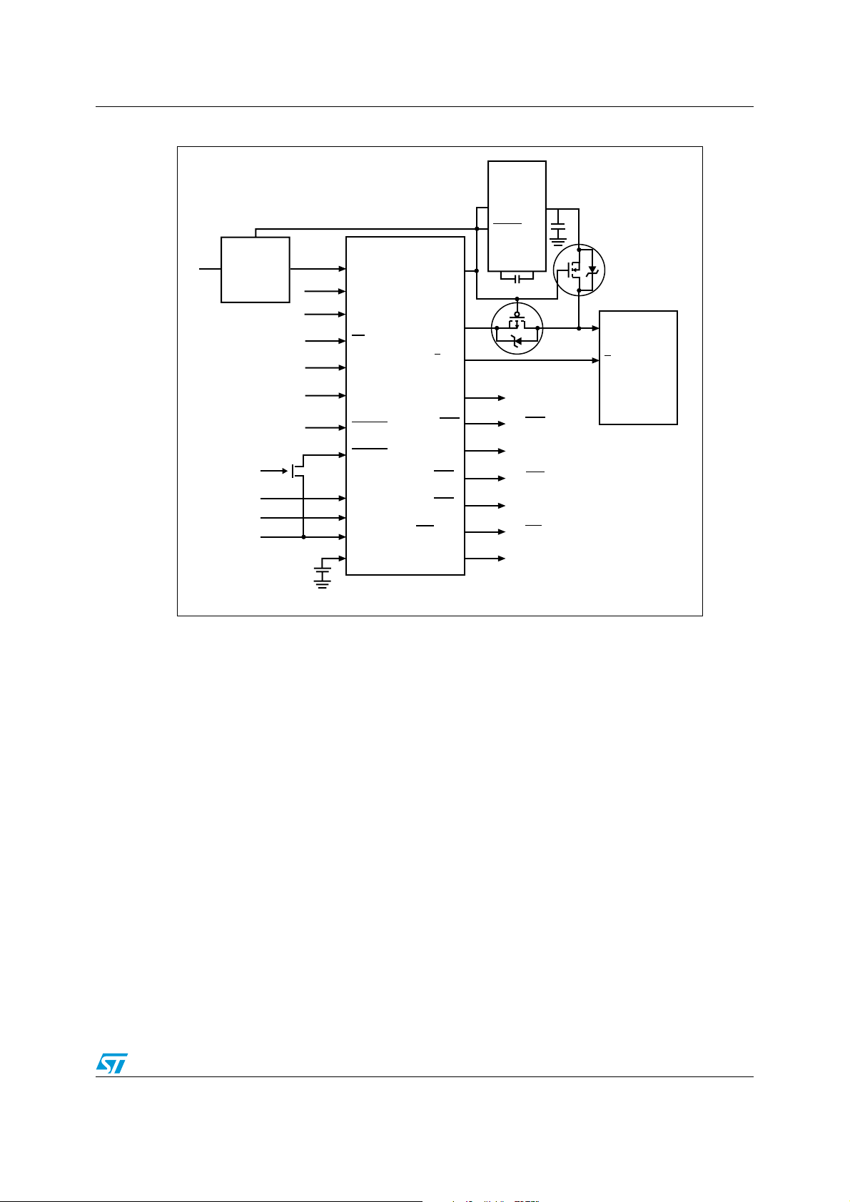
Clearing the external memory with an external charge pump
An external charge pump device should be used with the M41ST87 to drive VCC of the
SRAM to a negative voltage during the tamper condition. Figure 1 on page 3 shows how to
connect this circuit. When using the M41ST87 with the charge pump device, the user must
also provide two additional MOSFETs to isolate the V
(OUT) of the charge pump during normal operation, and from V
during the tamper condition. During normal operation the TP
disabling the charge pump. When disabled, the output of most charge pumps will be forced
to Ground. In order to allow proper operation of the SRAM, MOSFET(1) must be “off” to
isolate V
of the SRAM from the charge pump output. At this same time, P-channel
CC
MOSFET(2) will be “on” to provide the supply voltage for the SRAM.
During a tamper condition, the TP
signal will be forced high, controlling the inhibit pin of
CLR
the DC regulator. This will put the regulator in standby mode for t
clear timing where the regulator will be switched off for 1, 4, 8, or 16 seconds, depending on
the setting of the CLRPW1 and CLRPW0 bits in the register. The TP
the charge pump. When the charge pump is enabled, OUT generates a negative voltage on
the V
M41ST87 must be isolated from the V
pin of the SRAM (for a programmable period of time), causing data corruption. The
CC
of the SRAM to avoid data corruption of the
CC
M41ST87 due to forward biasing of the parasitic diode of the M41ST87 V
accomplished by using the TP
signal to turn the N-channel MOSFET(1) “on,” while
CLR
turning the P-channel MOSFET(2) “off.”
of the M41ST87 from the output
OUT
of the M41ST87 device
OUT
signal will be forced low,
CLR
. The t
CLR
CLR
signal also enables
CLR
OUT
is the tamper
output. This is
2/9
Page 3
AN1879 Description
Figure 1. Circuit connection
Inverting
Charge
Inhibit
V
IN
5V
Regulator
Pump
OUTIN
SHDN
M41ST87Y/W
V
CC
V
CC
TP1
TP2
EX
SCL
WDI
TP
CLR
IN
IN
V
E
OUT
CON
SDA
CAP+ CAP–
C1
C2
(2)
Negative Output
(–1 x VIN)
(1)
V
CC
E
Low-Power
SRAM
Pushbutton
Reset
1. N-channel MOSFET
2. P-channel MOSFET
RSTIN1
RSTIN2
PFI
1
PFI
2
V
SS
V
BAT
RST
SQW/FT
PFO
PFO
IRQ/OUT
F
32k
To RST
To LED Display
1
2
To NMI
To INT
To 32kHz
AI07804
3/9
Page 4

RAM clear data AN1879
RAM clear data
Depending on the process technology used to manufacture the external SRAM, clearing the
memory may require varying durations of negative potential on the V
device allows the user to program the time needed for their particular application. The
control bits CLRPW0 and CLRPW1, located in the day register, determine the duration of
the t
pulse width during a tamper event (see Figure 2). Thus, users can control the
CLR
voltage and duration of the negative pulse enabling them to configure the circuit for many
different LPSRAMs.
At STMicroelectronics, we have evaluated several different SRAMs with different densities
and found that we were able to corrupt the memory with certain minimum duration
(1 second) negative pulse widths (see Ta bl e 1 ).
Figure 2. Tamper output timing
pin. The M41ST87
CC
TP
CLR
RST
V
OUT
IRQ/OUT
E
CON
t
CLRD
t
CLR
t
rec
(1)
(3)
Tamper
Event
(TB Bit set)
High-Z
High-Z
(2)
(4)
AI07083
4/9
Page 5

AN1879 RAM clear data
Table 1. RAM clear data with different vendors
SRAM Cypress Hyundai Hitachi Cypress Hyundai Samsung ST
Density 1 Mb 1 Mb 4 Mb 4 Mb 4 Mb 4 Mb 4 Mb
2.55 2.55 2.55 2.55 2.55 2.55 2.55 V
2.390 2.390 2.426 2.425 2.400 2.423 2.413 V
0000000µA
925.0 582.0 567.0 578.0 752.0 492.0 587.0 nA
–259.2 –267.2 –272.7 –287.7 –275.9 –382.0 –283.2 µA
2.042 2.030 2.022 2.000 2.018 2.010 2.010 V
316.8 323.0 327.4 339.5 329.8 335.0 336.0 µA
–0.522 –0.488 –0.465 –0.397 –0.449 –0.425 –0.421 V
319.2 325.0 329.6 340.8 331.6 336.5 337.4 µA
Before
Tampe r
During
Tampe r
(1)
V
V
OUT
I
To t a l I
I
SRAM
V
I
V
SRAM
To t a l I
BAT
IN
BAT
IN
IN
BAT
Status Corrupted
1. Typically some SRAMs would take > 10 seconds when VCC is taken to VSS at 25°C to corrupt the memory.
Unit
Keys:
V
= Battery voltage
BAT
V
= Voltage output
OUT
I
= Current into charge pump before and during tamper condition
IN
To t a l I
I
SRAM
V
IN
V
SRAM
= Battery backup current of both the M41ST87 and the SRAM
BAT
= Current sink into the external SRAM
= Voltage at the charge pump input during tamper condition
= Negative voltage produced by the charge pump at SRAM VCC during tamper condition
5/9
Page 6

Tamper timestamp AN1879
Tamper timestamp
When the device is tampered with, and regardless of which tamper occurs first, a time
stamp freezing the update of the clock registers will occur to let the user know when it was
tampered with. The tamper bits (TB1 or TB2 in the flag register) will be set immediately.
Therefore, when tampering occurs, the user may elect to first read the time registers to
determine exactly when the tamper event occurred, then read the flag register to see which
tamper condition was triggered. The clock will update to the current time after resetting the
TEB bit in the tamper registers. The appropriate TEB bit must always be reset to '0' in order
to read the current time. The tamper detect function operates in V
backup.
as well as in battery
CC
6/9
Page 7

AN1879 Conclusion
Conclusion
With the increasing frequency of credit card fraud and identity theft, ST is leading the way
protecting this sensitive data with its new line of secure RTCs. This sensitive data is stored
in internal or external memory of most devices like ATM machines or POS terminals. The
M41ST87 solution can provide early detection when these devices have been tampered
with and clear the RAM before the intruder can access this data.
7/9
Page 8

Revision history AN1879
Revision history
Table 2. Document revision history
Date Revision Changes
04-Feb-2004 1 First edition
12-Apr-2004 2 Reformatted; update vendor SRAM information (Ta bl e 1 )
03-Jun-2004 3 Correct drawing (Figure 1)
Reformatted document; updated cover page, Clearing the
16-Jan-2009 4
external memory with an external charge pump, Figure 1, and
RAM clear data.
8/9
Page 9

AN1879
Please Read Carefully:
Information in this document is provided solely in connection with ST products. STMicroelectronics NV and its subsidiaries (“ST”) reserve the
right to make changes, corrections, modifications or improvements, to this document, and the products and services described herein at any
time, without notice.
All ST products are sold pursuant to ST’s terms and conditions of sale.
Purchasers are solely responsible for the choice, selection and use of the ST products and services described herein, and ST assumes no
liability whatsoever relating to the choice, selection or use of the ST products and services described herein.
No license, express or implied, by estoppel or otherwise, to any intellectual property rights is granted under this document. If any part of this
document refers to any third party products or services it shall not be deemed a license grant by ST for the use of such third party products
or services, or any intellectual property contained therein or considered as a warranty covering the use in any manner whatsoever of such
third party products or services or any intellectual property contained therein.
UNLESS OTHERWISE SET FORTH IN ST’S TERMS AND CONDITIONS OF SALE ST DISCLAIMS ANY EXPRESS OR IMPLIED
WARRANTY WITH RESPECT TO THE USE AND/OR SALE OF ST PRODUCTS INCLUDING WITHOUT LIMITATION IMPLIED
WARRANTIES OF MERCHANTABILITY, FITNESS FOR A PARTICULAR PURPOSE (AND THEIR EQUIVALENTS UNDER THE LAWS
OF ANY JURISDICTION), OR INFRINGEMENT OF ANY PATENT, COPYRIGHT OR OTHER INTELLECTUAL PROPERTY RIGHT.
UNLESS EXPRESSLY APPROVED IN WRITING BY AN AUTHORIZED ST REPRESENTATIVE, ST PRODUCTS ARE NOT
RECOMMENDED, AUTHORIZED OR WARRANTED FOR USE IN MILITARY, AIR CRAFT, SPACE, LIFE SAVING, OR LIFE SUSTAINING
APPLICATIONS, NOR IN PRODUCTS OR SYSTEMS WHERE FAILURE OR MALFUNCTION MAY RESULT IN PERSONAL INJURY,
DEATH, OR SEVERE PROPERTY OR ENVIRONMENTAL DAMAGE. ST PRODUCTS WHICH ARE NOT SPECIFIED AS "AUTOMOTIVE
GRADE" MAY ONLY BE USED IN AUTOMOTIVE APPLICATIONS AT USER’S OWN RISK.
Resale of ST products with provisions different from the statements and/or technical features set forth in this document shall immediately void
any warranty granted by ST for the ST product or service described herein and shall not create or extend in any manner whatsoever, any
liability of ST.
ST and the ST logo are trademarks or registered trademarks of ST in various countries.
Information in this document supersedes and replaces all information previously supplied.
The ST logo is a registered trademark of STMicroelectronics. All other names are the property of their respective owners.
© 2009 STMicroelectronics - All rights reserved
STMicroelectronics group of companies
Australia - Belgium - Brazil - Canada - China - Czech Republic - Finland - France - Germany - Hong Kong - India - Israel - Italy - Japan -
Malaysia - Malta - Morocco - Singapore - Spain - Sweden - Switzerland - United Kingdom - United States of America
www.st.com
9/9
 Loading...