


AN1830
APPLICATION NOTE
ACHIEVING HIGH ACCURACY AND 13-BIT RESOLUTION
WITH ST7LITE2 ADC
1 INTRODUCTION
The purpose of this application note is to show users of the ST7LITE2 ADC how to achieve 13bit resolution with the internal amplifier. It also explains the software methodology, which can
be applied to find and cancel the amplifier offset error. A reference application is shown with
implementation of hardware and software filtering techniques (using an averaging algorithm)
to minimize the ADC error.
Please note the data provided with this application note is for reference only, measured in a
lab under typical conditions (unless specified otherwise) and not tested in production.
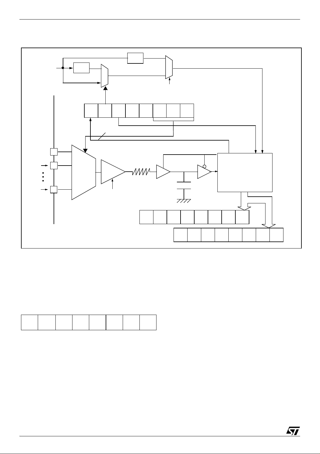
2 ST7LITE2 ADC OVERVIEW
The ST7LITE2 features a 10-bit successive approximation converter with internal sample and
hold circuitry. The ADC is connected to 7 multiplexed analog input channels which allow 7 pins
on Port B to be used as input for the ADC. The ADC can be turned ON/OFF using the ADON
bit, which can help to reduce consumption when not in use.
In addition to this it also provides an internal amplifier which can be used for small signal amplification.
2.1 ADC FUNCTIONALITY
The ADC can be connected to any of the analog channels by using the CH[2:0] bits in the ADCCSR Register. This analog input is connected to internal sample and hold circuitry. The
output of which is then converted into a 10-bit digital result via successive approximation (refer
Figure 1). The result of the conversion is stored in a 10-bit Data Register (ADCDRH + AD-
to
CDRL).
The analog supply pins V
DDA
and V
are the same as VDD and VSS for ST7LITE2.
SSA
Rev. 1.0
AN1753/0405 1/15
1
ACHIEVING HIGH ACCURACY AND 13-BIT RESOLUTION WITH ST7LITE2 ADC
Figure 1 ADC Block Diagram
AIN0
AIN1
AINx
f
CPU
DIV 2
ANALOG
MUX
0
1
3
x 1 or
x 8
AMPSEL
bit
ADCDRH
DIV 4
R
0
ADC
1
0
SLOW
bit
CH2 CH1EOC SPEED ADON 0 CH0
HOLD CONTROL
f
ADC
ADCCSR
C
ADC
ADCDRL 00 0
ANALOG TO DIGITAL
CONVERTER
D4 D3D5D9 D8 D7 D6 D2
AMP
CAL
SLOW
AMP
SEL
D1 D0
2.1.1 ADC Registers
The ADC functionality is driven using 3 main registers ADCCSR, ADCDRH and ADCDRL.
These are described below.
CONTROL/STATUS REGISTER (ADCCSR)
7 0
EOC SPEED ADON 0 0 CH2 CH1 CH0
This is a read/write register used to:
- Select the analog input channel by using bits CH[2:0]
- Turn the ADC ON / OFF (ADON)
- Select the ADC clock speed (SPEED)
- Obtain the status of conversion complete cycle (EOC)
2/15
2

ACHIEVING HIGH ACCURACY AND 13-BIT RESOLUTION WITH ST7LITE2 ADC
DATA REGISTER HIGH (ADCDRH)
7 0
D9 D8 D7 D6 D5 D4 D3 D2
This read only register provides MSB D[9:2] of the A/D conversion result.
AMP CONTROL/DATA REGISTER LOW (ADCDRL)
7 0
0 0 0
AMP
CAL
SLOW
AMP-
SEL
D1 D0
The read/write register can be used to:
- Provide LSB D[1:0] of the A/D conversion result.
- Select amplifier functionality: Amplifier select and Calibration (AMPSEL and AMPCAL)
- To configure f
along with the SPEED bit in the ADCCSR register (SLOW)
ADC
For a detailed description of each bit, refer to the ST7LITE2 datasheet.
2.2 UNDERSTANDING THE ADC INTERNAL AMPLIFIER
The purpose of the amplifier is to amplify an input voltage at analog input by a factor of 8. The
amplifier output is fed to the ADC. The amplifier introduces an offset at the output (
V
OFFSET
).
Thus the output becomes:
V
(Amplifier) = V
OUT
OFFSET
+ 8 x V
IN
where,
V
OFFSET
is the output offset voltage of the amplifier.
VIN is the amplifier input voltage (= AINx). Its range depends on the VDD supply voltage.
The amplifier is switched ON by the ADON bit in the ADCCSR register, so no additional startup time is required when the amplifier is selected by the AMPSEL bit.
You can also switch between the direct input and the amplified input i.e. the output of the amplifier can be either equal to its input or equal to the amplified output. This is controlled by the
control signal AMPSEL.
3/15
ACHIEVING HIGH ACCURACY AND 13-BIT RESOLUTION WITH ST7LITE2 ADC
2.2.1 AMPLIFIER OUTPUT OFFSET(V
OFFSET
): A Design Factor
A deliberate offset has been introduced in the design of the ST7LITE2 amplifier because in its
absence, for the 0V input, the amplifier goes into saturation and the final stage driver transistor
inside the amplifier can’t drive the capacitive load inside the ADC within the sampling period.
This phenomenon also leads to nonlinearity in the transfer curve around 0V input. By introducing the offset, the driver transistor is kept in the active region and this problem is avoided.
Therefore the amplifier offset is a design factor and not an error.
2.2.1.1 AMPLIFIER OFFSET VARIATION WITH RESPECT TO TEMPERATURE
One more important point is offset variation with respect to temperature. The offset is quite
sensitive to temperature variations. In order to ensure a good reliability in measure
ments, the offset must be recalibrated periodically i.e. may be after “N” seconds while ap-
plication is running depending on application requirement and temperature variation.
Table 1 Typical offset variation at 5V VDD with respect to temperature (1LSB= 4.88mV)
Temperature in 0C -45 -20 +25 +90
Error in LSB -12 -7 0 +13
2.2.2 AMPLIFIER GAIN
-
The typical gain of the amplifier is 8 by design, which is a ratio result of 2 on-chip resistors. The
mismatch in these 2 resistors can create gain error, depending on the voltage coefficient and
0
temperature. The measured gain error, including ADC inaccuracies is around 6% at 25
C.
2.2.3 TOTAL UNADJUSTED ERROR (TUE)
The TUE is a maximum deviation between the actual and the ideal transfer curves.
Table 2 below shows the Total Unadjusted Error for different VDD and V
IN (Max)
when the amplifier is ON without applying any software or hardware filtering over the temperature range –
40°C to +90°C. This is a global TUE since it includes ADC, Amplifier gain, Application and
Offset Errors. This can be reduced using the method explained in
Section 3.
Table 2 Total Unadjusted Error (Temperature: –40°C to +90°C)
V
DD
VIN
(Max)
TUE
3.6V 350mV ± 10 LSB
5.0V 500mV ± 10 LSB
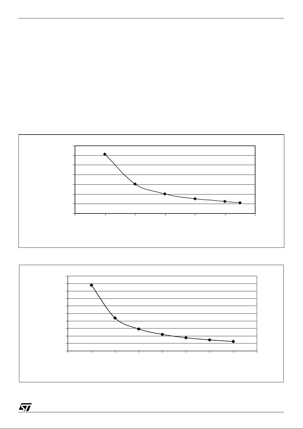
2.2.4 TOTAL ERROR IN PERCENTAGE (TE%)
This section presents 2 graphs showing the total precision error with respect to VIN for TUE
equal to ±10 LSB. The graphs (
Figure 2 and Figure 3) show the variation in error with respect
to VIN.
4/15
ACHIEVING HIGH ACCURACY AND 13-BIT RESOLUTION WITH ST7LITE2 ADC
V
The % TE increases for lower voltages, therefore it is recommended that you use the right
voltage range depending on the supply voltage V
. The formula used to calculate TE is:
DD
Total Error (TE) in worst case conditions = Global TUE / ((VIN x Typical gain) / 1LSB
x100%
Where, Global TUE=±10LSB
Typical Amplifier Gain = 8
1LSB
1LSB
for 5V VDD = 4.88mV
ideal
for 3.6V VDD= 3.5mV
ideal
Figure 2 Worst Case Total Error % @ 5V
7
6
5
4
3
TE%
2
1
0
0 0.1 0.2 0.3 0.4 0.5 0.6
ideal
)
Figure 3 Worst Case Total Error % @ 3.6V
10
9
8
7
6
5
TE %
4
3
2
1
0
0 0.05 0.1 0.15 0.2 0.25 0.3 0.35 0.4
in Max
Vin
5/15

ACHIEVING HIGH ACCURACY AND 13-BIT RESOLUTION WITH ST7LITE2 ADC
2.3 OPERATING MODES
The amplifier functions in different modes depending on the state of the digital control signals
AMPSEL and AMPCAL. These are explained below,
1) Analog input going directly to Amplifier output (Amplifier OFF)
When the amplifier is OFF, the ADC gets connected to the selected analog channel
through sample and hold circuitry. In this the case analog input goes directly to the Am
plifier output. The maximum and minimum input that can be given is VDD and VSS respectively with a resolution of 10 bits, which is equal to VDD/1024.
The state of control signals for this mode should be:
AMPSEL = 0
AMPCAL = 0
2) Analog input amplified and appearing at Amplifier output (Amplifier ON)
In this case amplifier is ON thus ADC input is,
-
V
(Amplifier) = V
OUT
OFFSET
+ 8 x VIN
The maximum voltage that can be applied at the analog input (VIN) is 500mV at VDD = 5V
and
350mV at VDD =3.6V with a resolution of 13 bits. The 13-bit resolution is because the
minimum signal that can be measured when the amplifier is ON, is 0.6103mV at 5V (e.g.
3
0.6103 x 8 (2
)= 4.8828 = 1LSB for 10-bit ADC) and 0.4394mV at 3.6V.
This maximum input voltage limitation is due to the nonlinearity of the amplifier as shown
in
Figure 4 in the amplifier transfer curve for 5V.
6/15

ACHIEVING HIGH ACCURACY AND 13-BIT RESOLUTION WITH ST7LITE2 ADC
Figure 4 Transfer curve for the amplifier when VDD = 5V
The state of control signals for this mode should be:
AMPSEL = 1
AMPCAL = 0
3) Amplifier output corresponds to 0V input (Offset Calibration)
To select this mode the state of the control signals for this mode should be:
AMPSEL= 1
AMPCAL = 1
Since V
at VIN = 0V is non-zero, therefore it has to be recorded once and then sub-
OUT
tracted from each of the amplified-and-converted output digital codes. This offset can be
recorded without having to supply 0V at V
.
IN
The above modes and the state of digital control signals required for each mode are shown in
Table 3.
Table 3 Operating Mode
Operating Mode
Amplifier OFF
AMPSEL AMPCAL
0 0
Amplifier ON
Offset Calibration
1 0
1 1
7/15

ACHIEVING HIGH ACCURACY AND 13-BIT RESOLUTION WITH ST7LITE2 ADC
3 TECHNIQUES TO IMPROVE THE ACCURACY
3.1 AMPLIFIER OFFSET COMPENSATION
The ADC must be offset-compensated because the output of the amplifier corresponding to
0V input is non-zero (equal to
served without having to apply 0V at the input. This is done by using the control signal AMPCAL.
The Amplifier takes the input voltage from the analog pad (after being multiplexed) and amplifies it by a factor of 8. In addition to this, it also introduces an offset at the output, which varies
from one part to another due to manufacturing process variations.
For this reason the ADC should be calibrated by configuring 0V once, storing it as an offset
and subtracting it from all amplified-and-converted digital codes.
Thus compensated ADC output = ADC Read data - OFFSET CNT (when AMPCAL=1)
Refer to Table 5 to understand how it is used.
V
OFFSET
). This output corresponding to 0V input can be ob-
3.2 SOFTWARE AVERAGING
Software averaging is a method used to reduce the effect of erroneous ADC output because
of noise or wrong conversion for fixed analog input.
As we take the average of several readings, these readings must correspond to the same analog input voltage. Take care that the analog input remains at the same voltage during the
time period when the conversions are done. Otherwise digital values corresponding to dif
ferent analog inputs will get added and introduce errors, i.e. the analog input should not
change between the different readings considered for the averaging.
-
8/15

ACHIEVING HIGH ACCURACY AND 13-BIT RESOLUTION WITH ST7LITE2 ADC
Figure 5 Averaging Algorithm
START
Initialize ADC variables, and select analog channel,
Read the ADC output registers after End of conversion
no
Total = 0
Start ADC
Add read value to Total
Num. of Conv.
= N?
yes
Average = Total / N
Use the Result
Table 4 is for reference only, representing the relation between the number of samples and
the accuracy. After 25 samples, it shows an LSB accuracy of 2. The number of samples to
choose depends on the application (noise level and timing) as these two are directly propor
tional. The disadvantage of having too many samples is that it takes more time to convert the
data.
Table 4 Number of Samples vs. Accuracy
-
Number of Samples Accuracy in LSB
10 4
20 3
25 2
30 2
40 2
50 2
9/15

ACHIEVING HIGH ACCURACY AND 13-BIT RESOLUTION WITH ST7LITE2 ADC
3.3 HARDWARE FILTERING
Figure 6 shows the hardware setup used in the reference application.
To minimize the effect of external noise (on the supply and input signal), shielded core wire is
used with capacitors C1 = C2 = 0.01µF, C3 = 1000µF, C4 =100µF. These capacitors should
be placed very close to the device input pins with short leads.
The values of these capacitors may vary from application to application, as they depend on
noise behavior and supply type.
Care should be taken regarding the shield; all grounds and shields in the application must be
connected in star format to earth.
In addition to this you can use a precision voltage reference
to reduce the effect of supply noise on conversion accuracy. This can have the disadvantage
of extra cost.
Figure 6 Hardware Setup
Supply
Ground
(VIN)
Analog Input
C1, C2 = Ceramic Capacitors
C3, C4 = Electrolytic Capacitors
+
C1
C2
C3
_
_
C4
+
V
DD
ST7LITE2
V
SS
AIN0/PBO
Application
Board
4 REFERENCE APPLICATION
The resolution of the ADC is 13-bit when the amplifier is ON, so even a small amount of noise
can create an error at output. This noise could be from the supply or the signal. To filter this out
and to obtain correct converted data it is suggested to use different software and hardware
techniques depending on your application requirements, like hardware filtering/shielding/soft
ware averaging/histogram etc.
However, taking into account this fact, the reference application has been provided showing
the implementation of software averaging, offset compensation and hardware filtering (refer to
Section 3.3 for hardware filtering).
-
10/15

ACHIEVING HIGH ACCURACY AND 13-BIT RESOLUTION WITH ST7LITE2 ADC
4.1 SOFTWARE FLOW
In software, firstly the AMPCAL and AMPSEL bits are set. Then the ADC is sampled for a defined number of times and averaged. This output is then stored in EEPROM as an offset. This
is then used in a program to get precise ADC output by subtracting it from subsequent ADC
samples (Refer to
Figure 7).
A total of 100 readings are taken and stored in EEPROM for the same analog input. And each
reading has a result of 25 averaged samples + offset compensation. These are to allow you to
compare it directly with respect to analog input.
However, the samples to be taken depend on the application so it is user-configurable. This
can be changed by using the “no_of_sample” value in software.
11/15

ACHIEVING HIGH ACCURACY AND 13-BIT RESOLUTION WITH ST7LITE2 ADC
Figure 7 Software Flow
START
Initialize variables
Initialize ADC in “Offset
samples & find out “Avg.”
.
Save “Avg” as an offset
Select AIN0 with Amplifier
CNT = 0
calibration” mode
Take “N” (=25) ADC
in EEPROM
ON
CNT > 100?
yes
no
Take “N” (=25) ADC
s
amples & find out “Avg.”
ADC CNT = Avg - Offset
(Offset compensation)
Store Avg. as ADC out-
put in EEPROM
CNT = CNT + 1
END
Please refer to Table 5 This represents ADC data with and without filtering in addition to data
before and after offset compensation. It shows that the ADC is highly accurate provided care
is taken to reduce application noise, as the resolution of ADC is 13-bit.
12/15

ACHIEVING HIGH ACCURACY AND 13-BIT RESOLUTION WITH ST7LITE2 ADC
Table 5 ADC Analysis (Before and After FILTER)
VIN (at AIN0)
in mV
50 82 145 136 87 78
200 328 393 383 335 325
400 656 718 710 660 652
Ideal ADC
CNT in
LSB
ADC output in LSB
ADCDRH + ADCDRL
Max Min Max Min
ADC Output with H/W and S/W filtering (in LSB)
50 82 141 140 83 82
200 328 388 383 330 325
400 656 716 714 658 656
Where:
OFFSET CNT = 58 in LSB (AMPCAL=1)
Ideal ADC CNT = (VIN x 8) /4.88 (at 5V)
ADC output in LSB (ADCDRH + ADCDRL) = ((V
x 8) + V
IN
OFFSET
ADC output in LSB (Off-
set Compensated)
) / 4.88
ADC output in LSB (Offset Compensated) = ADC output in LSB (ADCDRH + ADCDRL) -
OFFSET CNT
5 CONCLUSION
Overall, the ST7LITE2 ADC + Amplifier is a good price/performance trade-off with effective
resolution of 13-bit, which can be used in various applications where small signal amplification
is required with minimum hardware interface.
The accuracy of the ADC is also good, provided you take note of V
OFFSET
noise to a minimum for which you can use different techniques explained above. With these
techniques we are able to restrict the ADC error within ±3 LSB at room temperature with am
plifier ON.
An important thing to remember while using the ST7LITE2 amplifier is the “offset compensation”, which is mandatory due to the design of the device.
and keep external
-
13/15

ACHIEVING HIGH ACCURACY AND 13-BIT RESOLUTION WITH ST7LITE2 ADC
6 REFERENCES
To find out more about different ADC errors and compensating techniques, refer to the following application notes available on http://www.st.com
AN1711: Software Techniques for compensating ST7 ADC Errors
AN1636: Understanding and minimizing ADC conversion errors
7 EXAMPLE SOFTWARE
The complete software can be found on the ST Internet website in a zipped file format. It is intended for use only as an example. It is up to you to adapt it to your specific application requirements.
The source file is for guidance only. STMicroelectronics shall not be held liable for any direct,
indirect or consequential damages with respect to any claims arising from use of this software.
14/15

ACHIEVING HIGH ACCURACY AND 13-BIT RESOLUTION WITH ST7LITE2 ADC
“THE PRESENT NOTE WHICH IS FOR GUIDANCE ONLY AIMS AT PROVIDING CUSTOMERS WITH INFORMATION
REGARDING THEIR PRODUCTS IN ORDER FOR THEM TO SAVE TIME. AS A RESULT, STMICROELECTRONICS
SHALL NOT BE HELD LIABLE FOR ANY DIRECT, INDIRECT OR CONSEQUENTIAL DAMAGES WITH RESPECT TO
ANY CLAIMS ARISING FROM THE CONTENT OF SUCH A NOTE AND/OR THE USE MADE BY CUSTOMERS OF
THE INFORMATION CONTAINED HEREIN IN CONNECTION WITH THEIR PRODUCTS.”
Information furnished is believed to be accurate and reliable. However, STMicroelectronics assumes no responsibility for the consequences
of use of such information nor for any infringement of patents or other rights of third parties which may result from its use. No license is granted
by implication or otherwise under any patent or patent rights of STMicroelectronics. Specifications mentioned in this publication are subject
to change without notice. This publication supersedes and replaces all information previously supplied. STMicroelectronics products are not
authorized for use as critical components in life support devices or systems without express written approval of STMicroelectronics.
The ST logo is a registered trademark of STMicroelectronics.
All other names are the property of their respective owners
© 2005 STMicroelectronics - All rights reserved
STMicroelectronics group of companies
Australia – Belgium - Brazil - Canada - China – Czech Republic - Finland - France - Germany - Hong Kong - India - Israel - Italy - Japan -
Malaysia - Malta - Morocco - Singapore - Spain - Sweden - Switzerland - United Kingdom - United States of America
www.st.com
15/15
 Loading...