


AN1827
APPLICATION NOTE
IMPLEMENTATION OF SIGMA-DELTA ADC
WITH ST7FLITE05/09
INTRODUCTION
The purpose of this document is to describe how to implement a 10-bit Sigma-Delta A/D converter using a simple external circuit and a Sigma-Delta conversion program.
The ST7FLITE05(09) has an on-chip ADC with 8-bit resolution and an input range of 0-V
The external Sigma-Delta ADC described in this application is designed for relatively slow al-
ternating signals (0,2 - 5Hz) in the range 0 - 10mV(p-p). The focus of the project is to provide
good relative accuracy, repeatable parameters and simplicity, resulting therefore a low cost of
the device (in its simplest form, apart from the microcontroller, only three RC elements are
necessary).
CC
.
Rev. 1.0
AN1827/0304 1/11
1
IMPLEMENTATION OF SIGMA-DELTA ADC WITH ST7FLITE05/09
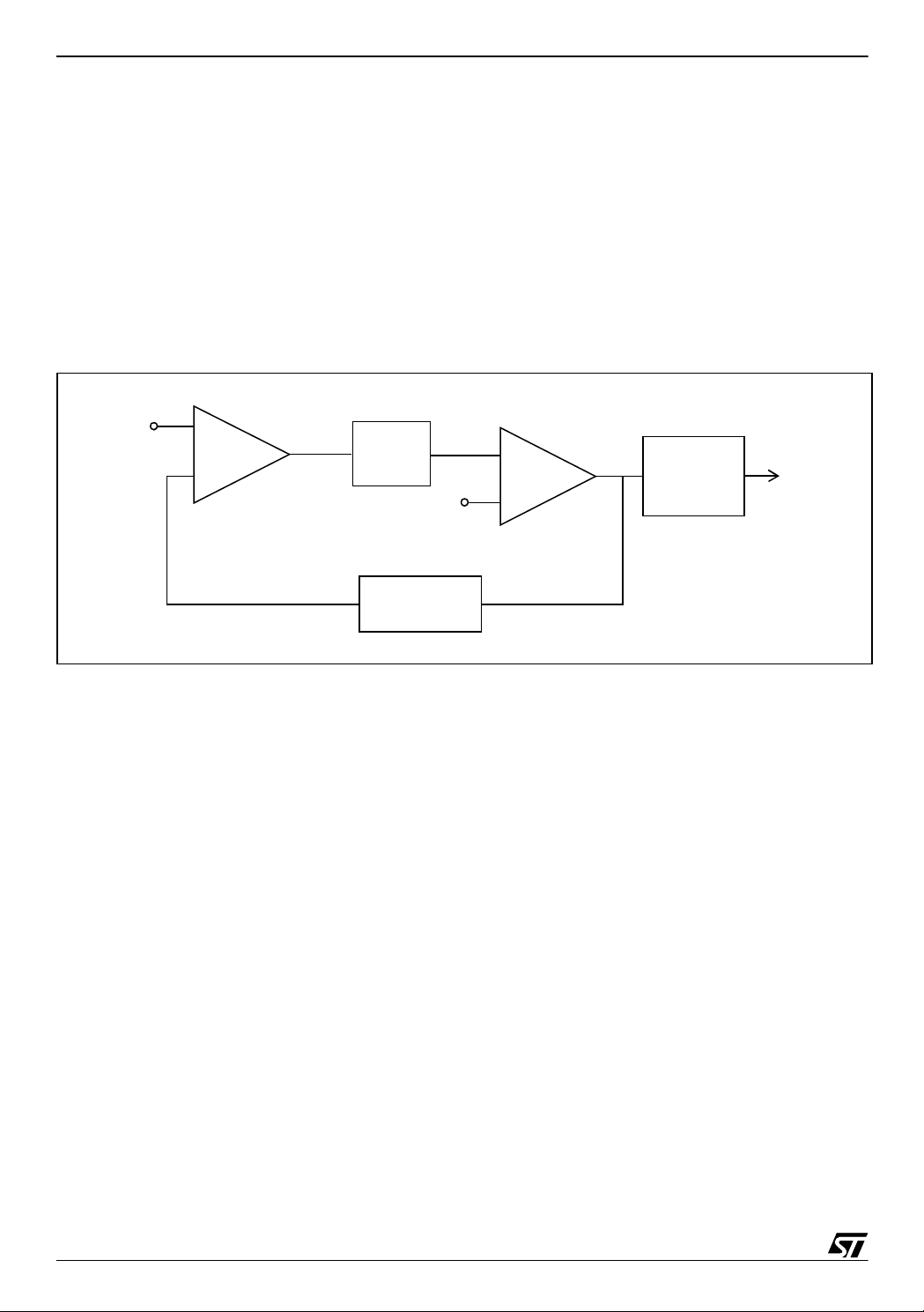
1 SIGMA-DELTA CONVERTER THEORY
The basic Sigma-Delta converter (Figure 1) is built of 2 basic circuits: a modulator and a digital
filter. In the modulator the input signal is summarised with the signal of negative feedback from
the D/A co nverter. The signal’s difference , after passi ng throug h the integr ating circu it,
reaches the input of the comparator, where it is compared to the r eference voltage (the comparator works as a 1-bit quantizator). The input signal from the comparator co ntrols the 1-bit
converter and reaches the input of the digital filter, which decreases flowability and transforms
the 1-bit stream into 10-bit words.
Figure 1. Sigma-Delta Conversion
+
∫
-
V
REF
+
-
DIGITAL
FILTER
1 BIT DAC
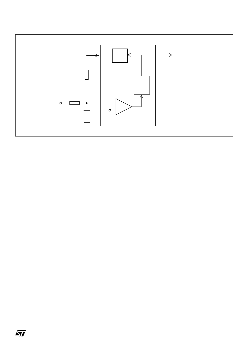
Figure 2 shows the general scheme of the m icrocon troller implementation. Within the system
the function of an integrator is fulfilled by the Ci capacitor, and the range of converted voltages
depends on the resistance ratio R1 and R2. The principle of operation is as follows: from the
moment of setting the high status on the output, the voltage on the Ci capa citor and simultaneously on the input of the comparator begins to rise. As soon as the reference voltage is
reached the output status is altered a nd th e vo ltage decr eases. After f alling below the r eference voltage the output status is altered to the high one and the cycle repeats. Provision of the
state of balance and the correct conversion of signal into its digital form is realised by a program-operated feedback loop and digital filter.
2/11
2
IMPLEMENTATION OF SIGMA-DELTA ADC WITH ST7FLITE05/09
Figure 2. Sigma-Delta Imp lementation with Microcontroller
SERIAL OUTPUT
PORT
I/O
R
2
FIRMWARE
R
V
IN
1
C
i
V
REF
+
-
COMPARATOR
3/11
IMPLEMENTATION OF SIGMA-DELTA ADC WITH ST7FLITE05/09
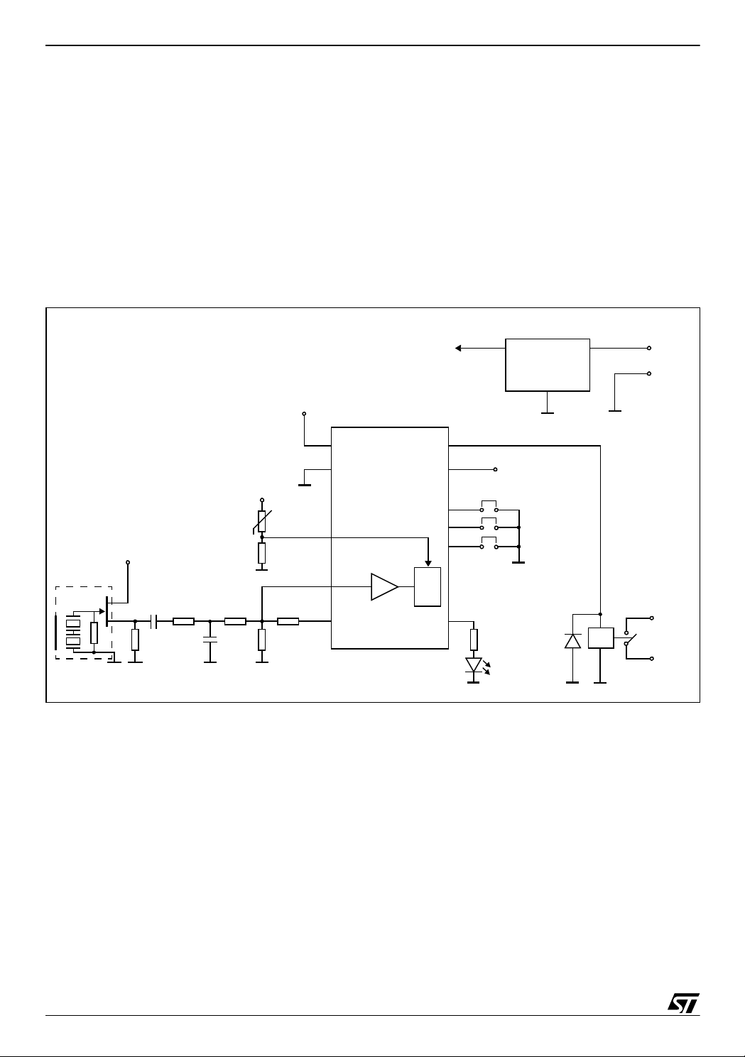
2 REALISAT ION WITH THE USE OF THE MICROCON TROLLER ST7FLI TE05(09)
The practical realisation of the Sigma-Delta converter has been used with our passive infrared
detector. A sensor of passive infrared c haracterise s with a low output vo ltage (belo w 10mV)
as well as with a usable range of frequ encies from 0,2Hz to 7Hz. Therefore the Sigma-D elta
converter is a perfect solution. It provides an a ccurate enough conversion of a signal in to its
digital form with use of a minimal number of external elements. That means simplicity of construction, relatively low production costs and good using properties.
Figure 3 presents the block diagram of the detector.
Figure 3. ST7FLITE05 interfacing with PIR Sensor
LD2980
TP
SERIAL OUTPUT
CONFIGURATION
POWER
OUTPUT
REL
ELEMENT PIR
VCC
V
CC
PB 0
PB 1
PB 4
ST7FLITE05
ANALOG
INPUT
ANALOG
INPUT
x8
OUTPUT
ADC
V
CC
PA 0
PA 1
PA 4
PA 5
PA 6
PA 7
A signal from the sensor passes through the capacitor to the input of the converter. The A/D
converter has been used as a comparator in the microcontroller as well as the source of the
reference voltage. By enabling the internal x8 amplifier, the amplitude of an output signal has
been decreased 20 times to provide correct operation of the amplifier. This allows a decrease
in the res ist o rs ’ value span in the sa me ratio and to increase the operational ac curacy of the
A/D converter working as a comparator. Additionally the temperature compensation of sensitivity has been introduced.
Figure 4 shows the work algorithm of the Sigma-Delta converter.
4/11

IMPLEMENTATION OF SIGMA-DELTA ADC WITH ST7FLITE05/09
Figure 4. Flow Chart (Sigma -Delt a Conversion)
A/D conversion from AIN1
channel, amplifier x8 included
U
>037h
AIN1
FalseTrue
Dlt_out:=0
inc Adc
True
Initiation of a
new conversion
Nw_adc := 1
Rez := Adc
Loop := 0
Adc := 0
inc Loop
Loop = 1024?
Dlt_out:=1
False
End of
interrupt
End of
interrupt
5/11

IMPLEMENTATION OF SIGMA-DELTA ADC WITH ST7FLITE05/09
3 THE DESCRIPTION OF THE SIGMA-DELTA CONVERSION PROGRAM
The Sigma-Delta conversion procedure is executed cyclically in an i nterr upt from the AT timer
with a period of 50µs. The result of the Sigma-Delta conversion (a 10-bit word) is achieved
every 1024 interrupts , that i s to say e very 51.2m s. The main loop of the progr am awaits the
Sigma-Delta conversion result and sends it through the RS serial interface to the computer.
The start of the Sigma-Delta conversion is preceded with clearing of the loop conversion
counter Loop_h, Loop_l and the result registry Adc_h, Adc_l.
At the first stage, the service routine of the AT timer interrupt clears the marker of request and
executes the A/D conversion from the AIN1 channel (the x8 amplifier is on). Following this, the
result of conversion i s c ompared wi th the constant value r epresented by the reference voltage
037h).
If, in the result of comparison, the voltage from the AIN1 c hannel is lower than the reference
voltage, then the B-Dlt port line will be set and the loop conversions counter will be increased.
Loop_h, Loop_l.
In a reverse situatio n, when the vo ltage from the AI N1 channe l is higher than the reference
voltage, the B-Dlt port line will be set to zero, and the Adc_h,Adc_l result registry as well as the
Loop_h, Loop_l. loop conversion counter will be increased.
The next task of the interrupt is to check whether the Loop_h, Loop_l loop conversion counter
has reached the value 1024. When the Loop_h, Loop_l loop conversion counter is lower than
1024, the service routine of the i nterrupt fi nishes. If thi s condition i s ful filled the v alue of the r esult registry is rewritten into the r esult Rez_h, Rez_l buffer and a request of a new result to the
main loop is set and the start of a new conversion is initiated (clearing of the Loop_h, Loop_l
counter and of the Adc_h,Adc_l.result registry)
The period of an AT timer interru pt is not critical . In the below ex ample, be cause o f the frequency of the signal fr om the passive infrared detector a nd the speed of R S comm unication
(19200bps), it has been defined at 50µs.
;**********************************************************************
;Listing of S-D conversion program.
;**********************************************************************
st7/
TITLE "pir.asm"
#INCLUDE "st72flt0.inc" ; definitions of registers st72lite
;**********************************************************************
;The program that realises the sigma/delta conversion
;sends the results of conversion to PC through the RS port
;**********************************************************************
;Definitions of variables
6/11

IMPLEMENTATION OF SIGMA-DELTA ADC WITH ST7FLITE05/09
;**********************************************************************
Rez_h equ $80 ; conversion result buffer H
Rez_l equ $81 ; conversion result buffer L
Loop_h equ $82 ; loop conversions counter H
Loop_l equ $83 ; loop conversions counter L
Adc_h equ $84 ; conversion result H
Adc_l equ $85 ; conversion result L
FLAGS0 equ $90 ; binary variables
Nw_adc equ 7 ; new data from the conversion
m50us equ 6 ; marker 50us
;**********************************************************************
;Definitions of constants
;**********************************************************************
;port A ; destination of bits in port A
RS equ 6
;**********************************************************************
;port B ; destination of bits in port B
Adc_in equ 1
Dlt_out equ 4
;**********************************************************************
;Processor initiation segment 'rom'
;**********************************************************************
INIT: sim
rsp
ld a,$FFDE
ld RCCR,a ; oscillator frequency calibrator RC
ld a,#%01000000 ; settings of ports
ld PADDR,a
ld a,#%01000000
ld PAOR,a
ld PADR,a
ld a,#%00010000
ld PBDDR,a
ld a,#%00010000
ld PBOR,a
ld PBDR,a
ld x,#$80 ; All RAM clearing (80-FF)
loop_clrRAM: clr (x)
inc x
jrne loop_clrRAM
ld a,#$0E ; initiation of an AT timer interrupt with
; the period of 50us
7/11

IMPLEMENTATION OF SIGMA-DELTA ADC WITH ST7FLITE05/09
ld ATRH,a
ld a,#$70
ld ATRL,a
ld a,#%00010010
ld ATCSR,a
rim
;**********************************************************************
;Main loop of the program
;**********************************************************************
IDLE: btjf FLAGS0,#Nw_adc,Idle ; waiting for the conversion result
bres FLAGS0,#Nw_adc ; new result
; sending the conversion result
; through RS
ld a,#$FF ; frame format:
call Send_rs ;0FFh,0FFh,Rez_H,Rez_L
ld a,#$FF
call Send_rs
ld a,Rez_h
call Send_rs
ld a,Rez_l
call Send_rs
jra IDLE
;**********************************************************************
;Interrupts
;**********************************************************************
; delta/sigma conversion
; sampling of 1 bit with period of 50us
; conversion result- 10 bit word, received every (1024*50us)=51,2ms
;**********************************************************************
timoverfl_rt: bres ATCSR,#2 ; cancelling of the interrupt re-
; quest
ld a,#00000100 ; adding the amplifier into the A/D
; processing
ld ADCCAMP,a
ld a,#%01100001 ; voltage measurement at AIN1
ld ADCCSR,a
loop_adc: btjf ADCCSR,#7,loop_adc
ld a,ADCDR
cp a,#$37 ; comparison U_ain1 z 037h
jrc set_Dlt
bres PBDR,#Dlt_out ; U_ain1>037h
inc Adc_l ; increase of the conversion result
8/11

IMPLEMENTATION OF SIGMA-DELTA ADC WITH ST7FLITE05/09
jrne inc_loop
inc Adc_h
jra inc_loop
set_Dlt: bset PBDR,#Dlt_out ; U_ain1<037h
inc_loop: bset FLAGS0,#m50us ; setting of a marker 50us
inc Loop_l ; increase of the samples counter
jrne tst_loop
inc Loop_h
tst_loop: ld a,Loop_l ; is the samples counter equal to
; 1024?
jreq tst_loopH
iret
tst_loopH: ld a,Loop_h
cp a,#$04
jreq ok_knw ; yes
iret
ok_knw: clr Loop_l ; conversion completed
clr Loop_h ; initiating of the loop conversion
; counter
ld a,Adc_h ; rewriting of the result into
; Rez_h,Rez_l
ld Rez_h,a
ld a,Adc_l
ld Rez_l,a
clr Adc_l ; initiating of the conversion re-
; sult variable
clr Adc_h
bset FLAGS0,#Nw_adc ; marker for IDLE (data ready)
iret
;**********************************************************************
spi_rt iret
lttimrtc_rt iret
ltimoutcmp_rt iret
timoutcmp_rt iret
lvd_rt iret
ext3_rt iret
ext2_rt iret
ext1_rt iret
ext0_rt iret
sw_rt iret
dummy iret
;**********************************************************************
;Procedures and subprograms
;**********************************************************************
9/11

IMPLEMENTATION OF SIGMA-DELTA ADC WITH ST7FLITE05/09
Send_rs: bres FLAGS0,#m50us ; procedure of RS data byte sending
call wait ; 19200bps,1b start,1b stop,8b data
bres PADR,#RS ; setting of a start bit
call wait
ld x,#$08
loop_snd: rrc a
call Send_bt ; setting of 8 data bits
dec x
jrne loop_snd
bset PADR,#RS ; setting of a stop bit
jra wait
Send_bt: jrc sd_H ; setting of a data bit at the port
bres PADR,#RS
jra wait
sd_H: bset PADR,#RS
wait: btjf FLAGS0,#m50us,wait ; latency for the duration of the
; data bit
bres FLAGS0,#m50us
ret
;**********************************************************************
;Interrupt vectors segment 'vectit'
;**********************************************************************
DC.W dummy ; FFE0-FFF1h location
spi_it DC.W spi_rt ; FFE2-FFE3h location
lttimrtc_it DC.W lttimrtc_rt ; FFE4-FFE5h location
ltimoutcmp_it DC.W ltimoutcmp_rt ; FFE6-FFE7h location
timoverfl_it DC.W timoverfl_rt ; FFE8-FFE9h location
timoutcmp_it DC.W timoutcmp_rt ; FFEA-FFEBh location
lvd_it DC.W lvd_rt ; FFEC-FFEDh location
DC.W dummy ; FFEE-FFEFh location
DC.W dummy ; FFF0-FFF1h location
ext3_it DC.W ext3_rt ; FFF2-FFF3h location
ext2_it DC.W ext2_rt ; FFF4-FFF5h location
ext1_it DC.W ext1_rt ; FFF6-FFF7h location
ext0_it DC.W ext0_rt ; FFF8-FFF9h location
DC.W dummy ; FFFA-FFFBh location
softit DC.W sw_rt ; FFFC-FFFDh location
reset DC.W INIT ; FFFE-FFFFh location
end
10/11

IMPLEMENTATION OF SIGMA-DELTA ADC WITH ST7FLITE05/09
“THE PRESENT NOTE WHICH IS FOR GUIDANCE ONLY AIMS AT PROVIDING CUSTOMERS WITH INFORMATION
REGARDING THE IR PRO DUCT S IN OR DER FO R THEM TO SAV E TIME . AS A RES ULT, STMIC ROEL ECTR ONI CS
SHALL NOT BE HELD LIABLE FOR ANY DIRECT, INDIRECT OR CONSEQUENTIAL DAMAGES WITH RESPECT TO
ANY CLAIMS ARISING FROM THE CONTENT OF SUCH A NOTE AND/OR THE USE MADE BY CUSTOMERS OF
THE INFORMATION CONTAINED HEREIN IN CONNECTION WITH THEIR PRODUCTS.”
Information furnished is believed to be accurate and reliable. However, STMicroelectronics assumes no responsibility for the consequences
of use of such information nor for any infringement of patents or other rights of third parties which may result from its use. No license is granted
by implic ation or oth erwise unde r any patent or patent r i ghts of STMi croelectroni cs. Speci fications me ntioned in this publicat i on are subject
to change without notice. This publication supersedes and replaces all information previously supplied. STMicroelectronics products are not
authorized for use as critical components in life su pport device s or systems without express written approval of STMicroelectronics.
The ST logo is a register ed t rademark of ST M i croelectroni c s.
All other nam es are the pro perty of their respective ow ners
© 2004 STMi croelectroni cs - All rights reserved
STMicroelectron i cs GROUP OF COMPANIES
Australia – Belgium - B razil - Canad a - China – Czech Republic - Finl and - France - Ger many - Hong Kong - India - Israel - Italy - Japan -
Malaysia - Malta - Morocco - Singapore - Spain - Sweden - Switzerland - United Kingdom - United States
www.st.com
11/11
 Loading...