

Page 1
Vref
AN1818
Reducing the Total No-Load Power Consumption of
Battery Chargers and Adapter Applications
1 Introduction
This paper describes how to reduce the power consumption, under no-load conditions, of battery
chargers and adapters by using STMi croelect ronics’s TSM famil y of seconda ry-side devices . This fam ily
of devices provides accurate voltage and current regulation, while incurring very low consumption at noload conditions. In fact, owing to these innovative, integrated devices, the total power consumption for the
entire system at no-load conditions can be reduced down to nearly 100mW. With the arrival of new power
consumption regulations, this capability is increasingly sought after.
The most innovative of S T’s devices are the TSM 101x family. These a re highly integrated solutions for
SMPS applications requiring CV and CC mode, integrating one voltage reference and two operational
amplifiers. The voltage reference combined with one operational amplifier makes them ideal voltage
controllers. The other operational am plifier, combined with the integrated voltage reference and a few
external resistors, can be used as a current limiter.
These products family are designed for use in battery chargers with a constant voltage and a limited
output current and in adapters.They can be used in every type of application requiring 0.5% and 1%
voltage reference precision.
2 Power dissipation under no-load conditions
In a typical system for battery charger and adapter applica tions, different factors contribute to the total
power dissipation under no-load conditions. However, in b road t erm s, the total power dissipation can be
divided into the dissipation o wing to the secondary-side (P
primary-side (P
).
in
) and the power dissipation owi ng to the
out
Secondary-side power dissipation
This article deals with reducing the secondary-side power dissipation, so let us begin by conside ring a
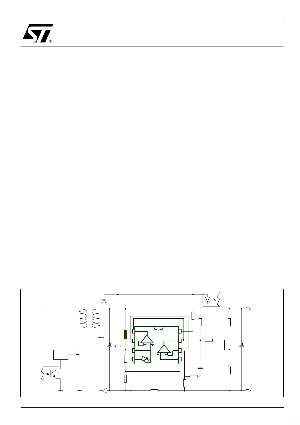
typical schematic of the secondary-side of an SMPS application, shown in Figure 1.
Figure1: Typical application using CC-CV Standard in SMPS
Cvc1
optocoupler
secondary side
R2
R1
OUT+
C3
OUT-
CC-CV Standard
OP1
Rsense
OP2
Ric2
Rlimit
R3
Rvc1
Cic1
Ric1
PWM
controller
optocoupler
primary s ide
D2
Rref
C1
C2
R4
R5
D1
AN1818/100 4 Revision 1 1/6
Page 2
AN1818 Power dissipation under n o-load conditions
The CC-CV (Constant Current - Constant Voltage) standard is a monolithic IC that includes one
independent op-amp and another op-amp for which the non-inverting input is wired to a 2.5V fixed voltage
reference. A good example of such a secondary-side device is ST’s TSM103W.
Normally the CC-CV voltage reference is “shunted”, meaning that the internal current generator requires
an external power supply in order to polarize and fix the voltage reference at 2.5V (V
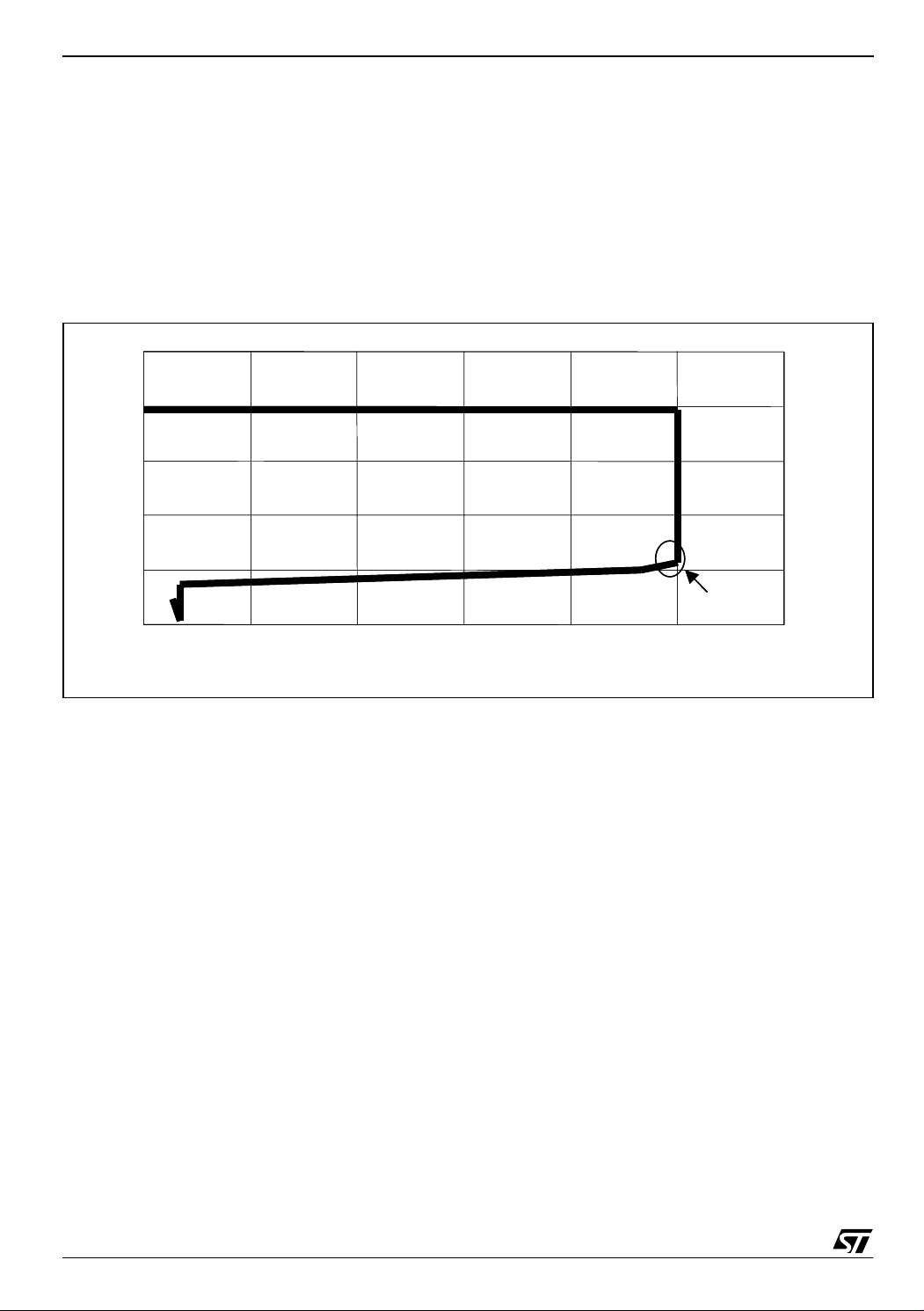
If we assume that V
is connected to a discharge ba ttery, the resulting ch aracteristic curve, V
out
shown in Figure 2.
- I
Figure2: Characteristic V
25
25
20
20
15
15
Vout (V)
Vout (V)
10
10
out
for adapter application
out
= 2.5V).
ref
out-Iout
, is
5
5
Vout_min in CC mode
0
0
0123456
0123456
Iout (A)
Iout (A)
Vout_min in CC mode
In Figure 2, we can see that the load charges gradually, by increasing the current and the voltage in order
to reach a minimal voltage drop. This gradual increase guarantees a limited and stable current. Following
this, the voltage value increases (while the current stays constant) up to the constant voltage value.
A typical adapter application will have V
out_max
= 20V (at no-load conditions) and V
= 5V (which is
out_min
the minimal voltage necessary to have a constant current).
In order to have V
out_min
= 5V, V
= 5V. If the minimum current value to bias V
cc_min
is 1mA, this means
ref
that:
R
ref
Therefore, in order to have V
= 5V, we must fix R
out_min
Now that we have fixed the value of R
I
V
outminVref
--------------------------------------- -
I
ref
, let's consider a no-load condition where V
ref
ref
–
1mA=
5V 2.5V–
------------------------ 2.5k Ω===
ref
1mA
= 2.5kΩ.
out_max
= 20V. It
follows that:
V
–
I
ref
outVref
-----------------------------
R
ref
20 2.5–
------------------ - 7 mA===
2.5
2/6
Page 3

Power dissipation under n o-load conditions AN1818
The total value of the secondary-side power dissipation is calculated using:
Equation 1
where
P
out
I
totIccIrefIopto
V
⋅=
outItot
++=
Equation 2
and I
This means that for a typical system at no-load conditions where V
I
opto
is the current needed to drive an optocoupler — typically about 1.5mA.
opto
= 20V, I
out
= 1.5mA, giving a secondary-side power dissipation (P
) equal to:
out
= 7mA, Icc = 1.5mA and
ref
Equation 3
P
out
V
outItot
⋅()V
outIrefIccIopto
++()⋅()20V 7mA 1.5mA 1.5mA++()⋅()20V 10mA⋅()200mW=====
Primary-side power dissipation
Now to turn our attention to the primary side of a typical adapter application. The primary side of an SMPS
application consists of a number of functional blocks (such as the PFC and PWM), each contributing to
the overall power consumption of the device. But in general, the overall power dissipation owing to
primary side functions can be assumed to be about 80mW under no-load conditions (for battery chargers
and adapters in the range 5W).
The key factor concerning the overall power consumpt ion on the primary-side is its efficiency rating,
which is at best about 50%. This means that to transfer 1mW of power to th e secondary side, 2mW of
power are generated in the primary side.
Returning to our cal culation in Equation 3 above, this means that if we require 200mW of power on the
secondary-side in no-load conditions, 400 mW will be generated on the primary side, and an additional
80mW will be necessary to drive the primary-side functions.
This relationship means that for any given redu ction in no-load power dissipation on the secondary side,
the beneficial effect will be twice as great on the primary side.
3/6
Page 4

AN1818 Optimizing your system
CC-
3 Optimizing your system
Typically, when one designs a battery charger or adapter application, a t arget power consumption is s et
for the application under no-load conditions. This target may be 500mW, or even 300mW, but until
recently, it seemed impossible to reach a no-load total power consumption of as low as 100mW.
In this section, we will look at three example syste ms:
a A typical secondary side configuration, as s een in Figure 1, and using a general-purpose second-
ary-side integrated circuit, such as ST’s TSM103.
b An advanced secondary side circuit schematic (see Figure 3), using an integrated circuit such as
ST’s TSM1011 which includes a self-polarizing voltage reference. The inclus ion of a self-polarizing voltage reference permits the elimination of the resistor R
of I
.
ref
c An advanced secondary -side schematic (see Figure 3) using a very advan ced integrated circuit,
ST’s TSM1012, which draws only 150µA under no-load conditions.
Figure3: Advanced secondary-side schematic for battery-charger/adapter application
Rlimit
D2
, and by consequence, eliminati on
ref
optocoupler
secondary side
PWM
controller
optocoupler
primary side
TSM1012
Vref Vcc
1 R3
5
R4
C2
C1
D1
3
R5
Rsense
2,5V
CV+
CC+
2
Ric2
Gnd
CV
CC
8
R2
28V
Out
7
4
CV-
6
Ric1
Rvc1
Cic1
Cvc1
C3
R1
In addition to considering the typical (Figure 1) and advanced (Figure 3) secondary side schematics,
there are now on the market optocoupl ers that need as little as 0.5mA . As we will see bel ow, u sing such
an optocoupler can allow power consumption to drop very low indeed.
4/6
Page 5

Optimizing your system AN1818
The following table summarizes the parameters for each of the above systems:
System A
“Typical
Configuration”
System B
“Optimized
Configuration”
System C
“Highly-Optimized
Configuration”
Secondary-side IC TSM103 TSM1011 TSM1012
V
ref
R
ref
I
ref
I
cc
I
(standard)
opto
I
= I
tot
V
out
+ Icc+ I
ref
under
opto
no-lo ad condi tion
P
out
P
in
Primaryfunction power
dissipation
2.5V (externally polarized) self-polarizin g self-polarizing
2.5kΩ none none
7mA none none
1.5mA 1mA 0.1mA
1mA 1mA 1mA
9.5mA 2mA 1.1mA
20V 20V 20V
190mW 40mW 22mW
380mW 80mW 44mW
80mW 80mW 80mW
Total Power Consumption
Target consumption window
460mW 160mW 124mW
<500mW <200mW <150mW
Using a low - po we r op t ocoupler:
(low power)
I
opto
I
tot
P
out
P
in
Primaryfunction power
dissipation
Total Power Consumption
Target consumption window
0.5mA 0.5mA 0.5mA
9mA 1.5mA 0.6
180mW 30mW 12mW
360mW 60mW 24mW
80mW 80mW 80mW
440mW 140mW 104mW
<500mW <150mW ~100mW
We can see from the above comparison that by using the TSM1012 and a low-consumption optocoupler,
an economy of nearly 80% in power consumption can be obtained relative to the “typical” CC-CV
secondary side s olutio n. And m ost impo rtant ly, i t is possibl e wi th this advance d syst em to desc end t o only
104mW in no-load conditions.
However, we can also see that only imp roving the optocouple r and retaining a standard secon dary-side
device (such as the TSM103) does not significantly improve the overall power consumption.
5/6
Page 6

AN1818 Conclusions
4 Conclusions
The new family of TSM101x secondary-s ide power management devices from STMi croelectronics for
adapter and battery charger applications open new horizons in total power consumption reductions.
These devices, coupled with innovative application schemes permit access to extremely efficient
solutions.
Information furnished is believed to be accurate and reliable. However, STMicroelectronics assumes no responsibility for the consequences
of use of such information nor for any infringement of patents or other rights of third parties which may result from its use. No license is granted
by implic ation or oth erwise unde r any patent or patent r i ghts of STMi croelectronics. Spec i fications me ntioned in this publication are subject
to change without notice. This publication supersedes and replaces all information previously supplied. STMicroelectronics products are no t
authoriz ed for use as crit i cal components in life support devices or systems wit hout express written approval of STMicroelectronics.
The ST logo i s a registered trademark of STM i croelect ronics
All other nam es are the prop erty of their re spective owners
© 2004 STMi croelectroni cs - All rights res erved
Australi a - Belgium - Brazil - Canad a - China - Czech Republic - Finl and - France - Germany - Hong Kong - India - Is rael - Italy - Ja pan -
Malaysia - M al ta - Morocco - Singapore - Sp ai n - Sweden - Switzerland - United Kingdom - United S tates of America
STMicroelectronics group of companies
www.st.com
6/6
 Loading...