

Page 1

AN1810
APPLICATION NOTE
STR71x BSPI COMMUNICATION
WITH M25P10-A SERIAL FLASH
INTRODUCTION
The aim of this application note is to present a practical example of communication using the
BSPI peripheral of the STR71x.
It shows an easy way of communicating between a STR71x microcontroller and a M25P10-A
SPI Serial Flash memory. The purpose is to perform, through BSPI, a write in the memory,
followed by a read of the written data.
The software implemented manages write and read operations between the STR71x BSPIinterface and the M25P10-A serial flash memory from STMicroelectronics.
1 APPLICATION OVERVIEW
This section summarizes the main features of the connection between STR71x and the SPI
Flash memory.
The Buffered Serial Peripheral Interface (BSPI) allows full-duplex, synchronous, serial communication between devices. A BSPI system may consist of a master and several slaves, or of
a system in which devices may be either master or slave. There is only one master at any time.
During BSPI transfer, data is simultaneously transmitted (shifted out serially) and received
(shifted in serially). Data is transmitted MSB first. The serial clock is used to synchronize the
data transfer during a sequence of eight clock pulses.
The bus signals are:
– The serial clock (SCLK).
– The MOSI (Master Out Slave In).
– The MISO (Master In Slave Out).
Another pin, the SSN pin (slave select), is needed to select Slave or Master Mode for each
device.
In this application note, the STR71x is always used as master (S1.SSN pin = high level). The
STR71x and SPI Flash interface set-up is shown in Figure 2.
Rev. 2.0
AN1810/0305 1/8
1
Page 2

STR71x BSPI COMMUNICATION WITH M25P10-A SERIAL FLASH
2 STR71X CONFIGURATION
2.1 I/O CONTROL
Five pins of the STR71x are used:
– The 4 (data and clock) BSPI pins (S1.SCLK, S1.MOSI, S1.MISO, S1.SSN)
– An output (P0.3) pin to select and deselect the M25P10-A
In this application, the P0.3 pin is used to drive the M25P10-A chip select pin. It is configured
as output push-pull (refer to the STR71x Reference Manual for more details).
2.2 BSPI PERIPHERAL
2.2.1 Baud Rates
Firstly, you have to choose the BSPI communication speed. As the clock is given by the master, you must configure the baud rate of the STR71x using the function
BSPI_ClockDividerConfig(BSPI1,Divider_factor_bits) or directly with the
BSPI1_CLK register (refer to STR71x Reference Manual for more details).
Note: In master mode, the Divider_factor_bits parameter must be an even number greater
than five (refer to STR71x Reference Manual for more details).
2.2.2 Clock Phase and Polarity
The next items to configure are the clock polarity and phase. The clock polarity CPOL controls the steady state value of the clock when no data is being transferred.
The clock phase CPHA selects on which clock transition the bit capture is made and consequently on which clock transition data is latched.
You must be careful because some devices do not allow all timing relationships. For instance,
the M25P10-A Serial Flash Memory device accepts only CPOL,CPHA = (0,0) or (1,1) configurations.
2/8
2
Page 3
STR71x BSPI COMMUNICATION WITH M25P10-A SERIAL FLASH
3 M25P10-A SERIAL FLASH MEMORY MANAGEMENT AND CONFIGURATION
3.1 SUMMARY DESCRIPTION
The M25P10-A is a 1 Mbit (128k * 8) Serial Flash Memory, with advanced write protection
mechanisms, accessed by a high speed SPI-compatible bus. The memory can be programmed 1 to 256 bytes at a time, using the Page Program instruction.
The write protect pin (W
) and the hold pin (H) are not used in our application (both are high
level).
3.2 STATUS REGISTER
The device has one status register which contains a number of control bits and status bits, as
shown in the following figure:
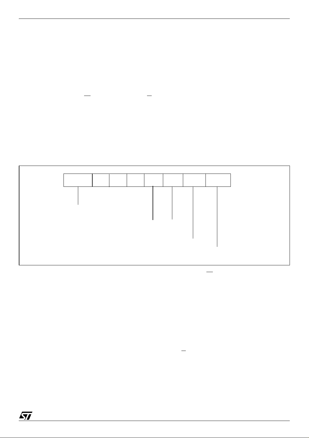
Figure 1. Status Register Control and Status Bits
000BP1SRWD BP0 WEL WIP
Status Register Write Protect
Block Protect Bit
Write Enable Latch Bit
Write in Progress Bit
The SRWD bit is operated in conjunction with the Write Protect (W
) signal.
The BP1 and BP0 bits in the status register can be used to write protect a block of memory. In
this application, both bits are cleared, allowing write access to all memory.
The WEL bit indicates the status of the write enable latch.
The WIP bit indicates whether the memory is busy with a Write Status register, Program or
Erase cycle.
3.3 INSTRUCTION SET
Prior to any operation, the device must be selected (S
pin at low level), then a one-byte
instruction code must be sent to the Serial Flash Memory. The device has a set of 11 instructions: (see Table 1, “Instruction Set,” on page 4).
3/8
Page 4

STR71x BSPI COMMUNICATION WITH M25P10-A SERIAL FLASH
Table 1. Instruction Set
Instruction Description One-byte In-
struction Code
WREN Write Enable 0000 0110 000
WRDI Write Disable 0000 0100 000
RDSR Read Status Register 0000 0101 001 to ∞
WRSR Write Status Register 0000 0001 001
READ Read Data Bytes 0000 0011 301 to ∞
FAST_READ
PP Page Program 0000 0010 3 0 1 to 256
SE Sector Erase 1101 1000 300
BE Bulk Erase 1100 0111 000
DP Deep Power-down 1011 1001 000
RES
Read Data Bytes at
Higher Speed
Release from Deep
Power-down, and Read
Electronic Signature
Release from Deep
Power-down
0000 1011 311 to ∞
10101011
Address
Bytes
031 to ∞
000
Dummy
Bytes
Data
Bytes
4/8
Page 5

STR71x BSPI COMMUNICATION WITH M25P10-A SERIAL FLASH
4 COMMUNICATION BETWEEN STR71X AND SERIAL FLASH MEMORY
The software included with this application note offers a set of functions allowing communication with the flash memory. The complete software can be found on the ST internet website. It
is a particular example and it is up to you to adapt it to your specific application.
4.1 HARDWARE DESCRIPTION
Two components were used for the application:
– 1 STR71x MCU device.
– 1 M25P10-A Serial Flash Memory
Figure 2. Hardware overview
C
1
100nF
M25P10-A
V
S
Q
V
cc
W
V
ss
V
ss
V
H
cc
C
D
cc
STR71x
P0.3
S1.SCLK
S1.MOSI
S1.MISO
S1.SSN
V
10K
cc
S1.SSN pin of STR71x is hardware driven (high level for a master device).
The S1.SCLK pin is connected to the serial clock pin (C) of the Serial Flash Memory.
The S1.MOSI pin to the serial input pins (D).
The S1.MISO pin to the serial output pins (Q).
pin of the Serial Flash Memory is connected to the P0.3 output pin of the STR71x.
S
4.2 SOFTWARE IMPLEMENTATION
In this application note the software modules are developed in C language, with RVDK envi-
ronment.
The software implemented in order to manage write and read operations between the
STR71x BSPI interface and the M25P10-A is described below.
It is made up of 4 parts:
5/8
Page 6

STR71x BSPI COMMUNICATION WITH M25P10-A SERIAL FLASH
1) Configuration of BSPI1 as a master,
2) Erase M25 SPI flash sector0,
3) Transmission of several bytes from Master to M25 SPI flash,
4) Read data already written to the M25 SPI flash.
4.2.1 Flowchart
The flowchart of the application is given below.
BEGIN
Initialization
Chip Select pin driven High / Low
Send a write enable instruction
Memory sector0 erase
Read status register
Send a write enable instruction
{
...
/*Initialize the STR71x BSPI1 & erase the
corresponding sector memory to be used.*/
/* Initialize STR71x BSPI device */
InitBSPIFlash ();
Chip_Select_M25_DISABLE;
Chip_Select_M25_ENABLE;
/* Send a write enable instruction to the memory */
M25_InstructionSend(M25_WREN);
/* Erase sector0 from the memory */
M25_SectorErase(M25_Sector0);
/* Send Read status register instruction */
M25_InstructionSend(M25_RDSR);
/* wait until all the sector is erased */
while((M25_DataReceive()&M25_WIP));
/* Write data to the memory and wait until
all the data is programmed*/
/* Send a write enable instruction to the memory */
M25_InstructionSend(M25_WREN);
Send PP instruction to the flash memory
Send data to the flash memory
Verify that all the data sent is programmed
A
6/8
/* Send page program instruction */
M25_InstructionSend(M25_PP);
/* wait until all the data is sent */
for (i=0;i<BufferSize;i++)
/* Send data to the memory */
M25_DataSend(SendBuffer [i]);
/* Send Read status register instruction */
M25_InstructionSend(M25_RDSR);
/* Wait until all the data sent is programmed */
while((M25_DataReceive()&M25_WIP));
Page 7

STR71x BSPI COMMUNICATION WITH M25P10-A SERIAL FLASH
A
/* Read from the flash memory the data already programmed*/
Send instruction in order to read data from the
memory
Send address memory to be read
Verify that all the data is read
END
/* send a Read Data Byte instruction */
M25_InstructionSend(M25_READ);
/* send address memory to be read */
M25_AddressSend(M25_ReadAddress);
/* read all the data already written */
for (i=0;i<BufferSize;i++)
ReceiveBuffer[i] = M25_DataReceive();
...
}
7/8
Page 8

STR71x BSPI COMMUNICATION WITH M25P10-A SERIAL FLASH
“THE PRESENT NOTE WHICH IS FOR GUIDANCE ONLY AIMS AT PROVIDING CUSTOMERS WITH INFORMATION
REGARDING THEIR PRODUCTS IN ORDER FOR THEM TO SAVE TIME. AS A RESULT, STMICROELECTRONICS
SHALL NOT BE HELD LIABLE FOR ANY DIRECT, INDIRECT OR CONSEQUENTIAL DAMAGES WITH RESPECT TO
ANY CLAIMS ARISING FROM THE CONTENT OF SUCH A NOTE AND/OR THE USE MADE BY CUSTOMERS OF
THE INFORMATION CONTAINED HEREIN IN CONNECTION WITH THEIR PRODUCTS.”
Information furnished is believed to be accurate and reliable. However, STMicroelectronics assumes no responsibility for the consequences
of use of such information nor for any infringement of patents or other rights of third parties which may result from its use. No license is granted
by implication or otherwise under any patent or patent rights of STMicroelectronics. Specifications mentioned in this publication are subject
to change without notice. This publication supersedes and replaces all information previously supplied. STMicroelectronics products are not
authorized for use as critical components in life support devices or systems without express written approval of STMicroelectronics.
The ST logo is a registered trademark of STMicroelectronics.
All other names are the property of their respective owners
© 2005 STMicroelectronics - All rights reserved
STMicroelectronics group of companies
Australia – Belgium - Brazil - Canada - China – Czech Republic - Finland - France - Germany - Hong Kong - India - Israel - Italy - Japan -
Malaysia - Malta - Morocco - Singapore - Spain - Sweden - Switzerland - United Kingdom - United States of America
www.st.com
8/8
 Loading...