

Page 1
AN1806
APPLICATION NOTE
Antenna (and Associated Components)
Matching-Circuit Calculation for the CRX14 Coupler
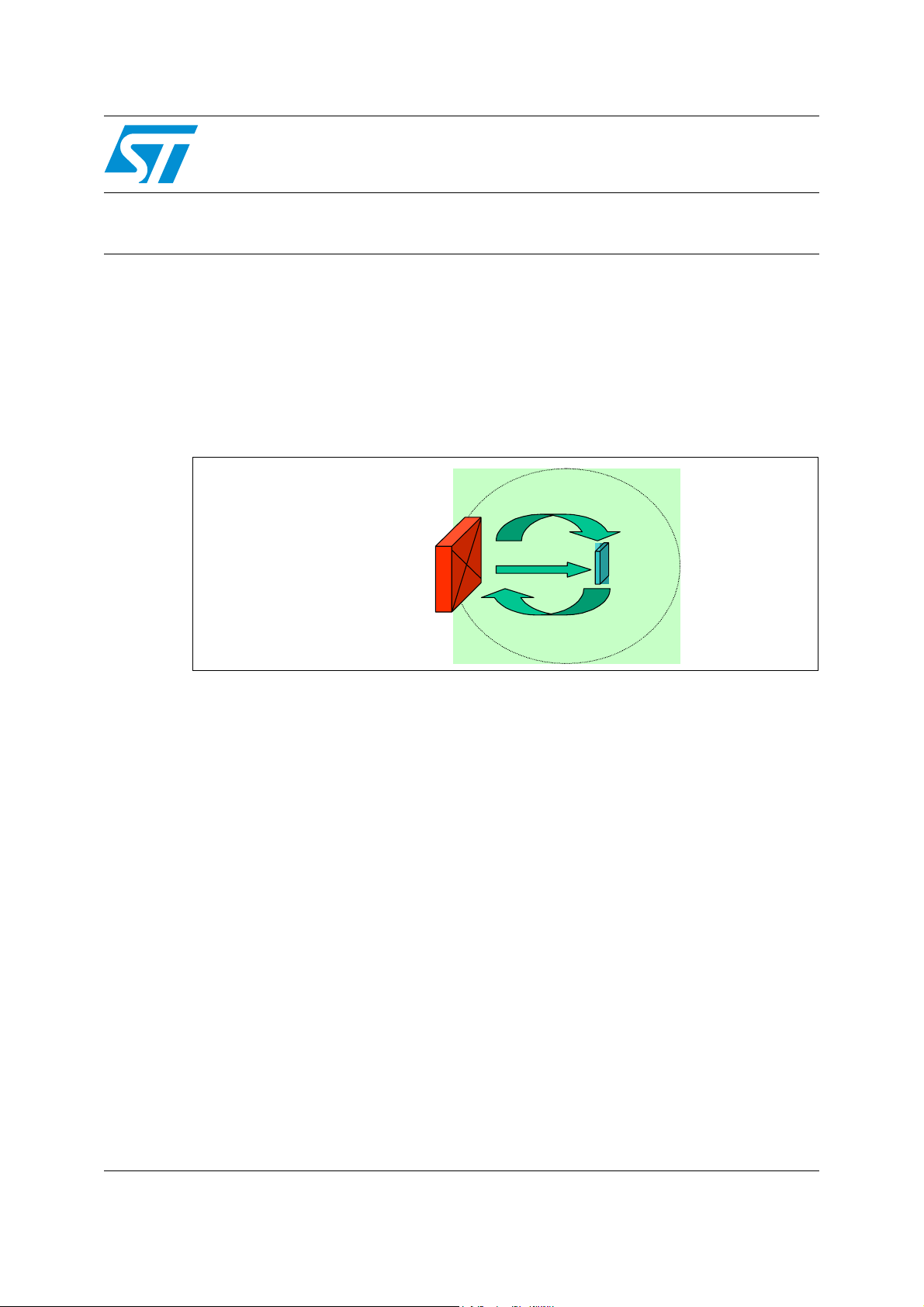
In the basic RFID system (as shown in Figure 1):
1. The Reader generates an electromagnetic field. This field is rectified to generate the
supply voltage inside the Tag.
2. The Reader transmits information to the Tag by modulating the carrier wave.
3. The Tag back-scatters the carrier wave, by modifying its own impedance thereby
perturbing the field, in order to transmit back information to the Reader.
Figure 1. Basic RFID System
Signal (2)
Reader/Writ er
Ante nna
Power (1)
Signal (3)
Tag
February 2006 Rev. 3 1/37
www.st.com
Page 2

Contents AN1806 - APPLICATION NOTE
Contents
1 CRX14 Contactless Coupler Chip from ST . . . . . . . . . . . . . . . . . . . . . . . 6
2 Short Range Contactless Memories from ST . . . . . . . . . . . . . . . . . . . . . 7
2.1 Low-end SR Family . . . . . . . . . . . . . . . . . . . . . . . . . . . . . . . . . . . . . . . . . . 7
2.2 Secure SRIX Family . . . . . . . . . . . . . . . . . . . . . . . . . . . . . . . . . . . . . . . . . . 7
3 Basic concepts and fundamental equations . . . . . . . . . . . . . . . . . . . . . 8
3.1 Electromagnetic Field . . . . . . . . . . . . . . . . . . . . . . . . . . . . . . . . . . . . . . . . . 8
3.2 Inductance, L, and the Antenna . . . . . . . . . . . . . . . . . . . . . . . . . . . . . . . . 10
3.3 Inductance of a Planar Rectangular Coil . . . . . . . . . . . . . . . . . . . . . . . . . 12
3.4 Magnetic Coupling Factor . . . . . . . . . . . . . . . . . . . . . . . . . . . . . . . . . . . . 13
4 Antenna . . . . . . . . . . . . . . . . . . . . . . . . . . . . . . . . . . . . . . . . . . . . . . . . . . 15
4.1 Matching Circuit . . . . . . . . . . . . . . . . . . . . . . . . . . . . . . . . . . . . . . . . . . . . 15
4.2 Current Calculation . . . . . . . . . . . . . . . . . . . . . . . . . . . . . . . . . . . . . . . . . . 18
4.3 VR Calculation . . . . . . . . . . . . . . . . . . . . . . . . . . . . . . . . . . . . . . . . . . . . . 19
4.4 Current Calculation . . . . . . . . . . . . . . . . . . . . . . . . . . . . . . . . . . . . . . . . . . 19
5 Designing an RFID application . . . . . . . . . . . . . . . . . . . . . . . . . . . . . . . 21
5.1 Using the Excel Spreadsheet . . . . . . . . . . . . . . . . . . . . . . . . . . . . . . . . . . 22
5.2 Step 1 . . . . . . . . . . . . . . . . . . . . . . . . . . . . . . . . . . . . . . . . . . . . . . . . . . . . 22
5.3 Step 2 . . . . . . . . . . . . . . . . . . . . . . . . . . . . . . . . . . . . . . . . . . . . . . . . . . . . 23
5.4 Step 3 . . . . . . . . . . . . . . . . . . . . . . . . . . . . . . . . . . . . . . . . . . . . . . . . . . . . 23
5.5 Step 4 . . . . . . . . . . . . . . . . . . . . . . . . . . . . . . . . . . . . . . . . . . . . . . . . . . . . 24
Appendix A Calculation details of serial-to-Parallel Conversion . . . . . . . . . . . . 26
5.6 Calculation of the Impedance of Equivalent Circuit
at the Second Resonance Frequency . . . . . . . . . . . . . . . . . . . . . . . . . . . 28
Appendix B Calculation Details of Current Calculation . . . . . . . . . . . . . . . . . . . 30
5.7 VR Calculation . . . . . . . . . . . . . . . . . . . . . . . . . . . . . . . . . . . . . . . . . . . . . 31
5.8 Current Calculation . . . . . . . . . . . . . . . . . . . . . . . . . . . . . . . . . . . . . . . . . . 32
2/37
Page 3

AN1806 - APPLICATION NOTE Contents
Appendix C Demo kit board. . . . . . . . . . . . . . . . . . . . . . . . . . . . . . . . . . . . . . . . . . 33
6 Revision history . . . . . . . . . . . . . . . . . . . . . . . . . . . . . . . . . . . . . . . . . . . 36
3/37
Page 4

List of tables AN1806 - APPLICATION NOTE
List of tables
Table 1. K1 and K2 values according to layout . . . . . . . . . . . . . . . . . . . . . . . . . . . . . . . . . . . . . . . . . 12
Table 2. Main Results. . . . . . . . . . . . . . . . . . . . . . . . . . . . . . . . . . . . . . . . . . . . . . . . . . . . . . . . . . . . 17
Table 3. Values of Capacitors. . . . . . . . . . . . . . . . . . . . . . . . . . . . . . . . . . . . . . . . . . . . . . . . . . . . . . 17
Table 4. Calculation steps . . . . . . . . . . . . . . . . . . . . . . . . . . . . . . . . . . . . . . . . . . . . . . . . . . . . . . . . 21
Table 5. Parameter values . . . . . . . . . . . . . . . . . . . . . . . . . . . . . . . . . . . . . . . . . . . . . . . . . . . . . . . . 23
Table 6. Parameter values for tuning . . . . . . . . . . . . . . . . . . . . . . . . . . . . . . . . . . . . . . . . . . . . . . . . 23
Table 7. Computed read range as a function of K and the H field . . . . . . . . . . . . . . . . . . . . . . . . . . 24
Table 8. Summary of the Main Results. . . . . . . . . . . . . . . . . . . . . . . . . . . . . . . . . . . . . . . . . . . . . . . 28
Table 9. Values of the Capacitors. . . . . . . . . . . . . . . . . . . . . . . . . . . . . . . . . . . . . . . . . . . . . . . . . . . 29
Table 10. Bill of Materials . . . . . . . . . . . . . . . . . . . . . . . . . . . . . . . . . . . . . . . . . . . . . . . . . . . . . . . . . . 34
Table 11. Document Revision History . . . . . . . . . . . . . . . . . . . . . . . . . . . . . . . . . . . . . . . . . . . . . . . . 3 6
4/37
Page 5

AN1806 - APPLICATION NOTE List of figures
List of figures
Figure 1. Basic RFID System. . . . . . . . . . . . . . . . . . . . . . . . . . . . . . . . . . . . . . . . . . . . . . . . . . . . . . . . 1
Figure 2. Circular Loop Antenna . . . . . . . . . . . . . . . . . . . . . . . . . . . . . . . . . . . . . . . . . . . . . . . . . . . . . 8
Figure 3. Magnetic Field as a Function of the Distance of the Tag from the Reader. . . . . . . . . . . . . . 9
Figure 4. Magnetic Field as a Function of the Antenna Radius . . . . . . . . . . . . . . . . . . . . . . . . . . . . . 10
Figure 5. Round Planar Spiral Coils. . . . . . . . . . . . . . . . . . . . . . . . . . . . . . . . . . . . . . . . . . . . . . . . . . 11
Figure 6. Planar Square, Hexagonal and Octagonal Spiral Coils . . . . . . . . . . . . . . . . . . . . . . . . . . . 11
Figure 7. User Interface Screen of the Planar Rectangular Coil Inductance Calculator . . . . . . . . . . 13
Figure 8. Real Circuit for the Antenna System on the Board. . . . . . . . . . . . . . . . . . . . . . . . . . . . . . . 15
Figure 9. Series-to-Parallel Circuit Equivalence . . . . . . . . . . . . . . . . . . . . . . . . . . . . . . . . . . . . . . . . 16
Figure 10. Parallel Equivalent Circuit. . . . . . . . . . . . . . . . . . . . . . . . . . . . . . . . . . . . . . . . . . . . . . . . . . 16
Figure 11. Equivalent Impedance (Z) Plotted against Frequency (f) . . . . . . . . . . . . . . . . . . . . . . . . . . 17
Figure 12. Coupling between One Tag and One Reader Antenna . . . . . . . . . . . . . . . . . . . . . . . . . . . 18
Figure 13. Equivalent Circuits . . . . . . . . . . . . . . . . . . . . . . . . . . . . . . . . . . . . . . . . . . . . . . . . . . . . . . . 19
Figure 14. Excel Configuration. . . . . . . . . . . . . . . . . . . . . . . . . . . . . . . . . . . . . . . . . . . . . . . . . . . . . . . 22
Figure 15. Basic Schematic . . . . . . . . . . . . . . . . . . . . . . . . . . . . . . . . . . . . . . . . . . . . . . . . . . . . . . . . . 25
Figure 16. Coupling factor model. . . . . . . . . . . . . . . . . . . . . . . . . . . . . . . . . . . . . . . . . . . . . . . . . . . . . 30
Figure 17. Equivalent circuits. . . . . . . . . . . . . . . . . . . . . . . . . . . . . . . . . . . . . . . . . . . . . . . . . . . . . . . . 31
Figure 18. Layout of Demo-kit Board. . . . . . . . . . . . . . . . . . . . . . . . . . . . . . . . . . . . . . . . . . . . . . . . . . 33
Figure 19. Component Implementation . . . . . . . . . . . . . . . . . . . . . . . . . . . . . . . . . . . . . . . . . . . . . . . . 3 4
5/37
Page 6

CRX14 Contactless Coupler Chip from ST AN1806 - APPLICATION NOTE
1 CRX14 Contactless Coupler Chip from ST
ST has designed the CRX14, a short range contactless coupler chip, compliant with the
ISO14443 type B proximity standard. The CRX14 generates a 13.56MHz signal. Designed
to deliver an RF power of 100mW, it operates in the Short Range on contactless memory
tags (provided that they, too, are compliant with ISO14443 type B).
The CRX14 features the ST anti-collision mechanism, which allows the reader to detect and
identify all the tags that are present in the operating range, and to access them individually.
Because the CRX14 implements the France Telecom-proprietary anti-clone function, the
reader can also perform authentication of tags that are equipped with the France Telecom
anti-clone capability.
The CRX14 coupler interf aces between:
● the memory tags, on one side, through input /output buffers and the ISO14443 type B
radio frequency protocol, and
● the system master processor, on the other side, through a 400kHz I
Operating from a 5V power supply, and delivered in a SO16N package, the CRX14 coupler
chip is an excellent solution for building contactless readers, embedded in the final
equipment, and offering a good co mpromise between operating range and cost.
2
C bus.
6/37
Page 7

AN1806 - APPLICATION NOTE Short Range Contactless Memories from ST
2 Short Range Contactless Memories from ST
All devices from the ST Short Range Contactless series are compliant with the ISO14443
type B standard. They a re accessible via a 13.56MHz carrier frequency, and support a data
transfer rate between tag and reader of 106kbit/s in both directions. All of them are totally
compatible with each other, in terms of tag protocol access. The series is sub-divided into
two families:
● Low-end SR Family
● Secure SRIX Family (equipped with anti-clone and anti-collision capabilities).
2.1 Low-end SR Family
SR176 is the first member of ST low-end short range family. It contains:
● 176 bits of EEPROM, organized as eleven 16-bit blocks, that can be write-protected
● a 64-bit UID, and
● a fixed 8-bit chip identifier.
2.2 Secure SRIX Family
SRIX is a family of highly secure devices that support the anti-clone capability, allowing tag
authentication. The system master processor sends an authenti cation request to ea ch of the
tags present in the CRX14’s field. Each tag runs its anti-clone algorithm to compute a
signature, and sends it back to the reader for an authentication check. The anti-clone
function helps fight against fraud, since any tag that does not belong to the system will
answer with a wrong signature.
The first member of the SRIX family is the SRIX4K, featuring 4096 bits of EEPROM
organized as 128 words of 32 bits. These are, in turn, organized in five main areas:
● One 5-word OTP z one , accessib le in user mode , whose bit s can only be s witche d from
1 to 0
● Two 32-bit binary counters that can only be decremented
● 121 words of user EEPROM, of which 9 can be individually write protected
● One 8-bit chip identifier that allows a reader to identify uniquely each tag present in its
field during the anti-collision operation
● One 64-bit read-only unique identifier (UID), programmed on the manufacturing line.
The family will be later extended to include a lower density, 512-bit, device.
7/37
Page 8
Basic concepts and fundamental equations AN1806 - APPLICATION NOTE
3 Basic concepts and fundamental equations
To calculate the characteristics of a RFID system, we need some definitions and
assumptions:
● The reader generates a tension
● This tension supplies the inductive antenna L
● A current I
flows through the antenna and creates a magnetic field defined at
R
distance x.
● This field is transformed into a supply voltage in the tag.
● When the tag is near the reader antenna, it modifies the antenna tuning.
● To calculate the real current, we need to calculate the mutual inductance M and the
coupling factor between the reader antenna L
● We can also calculate the range within which the tag receives enough magnetic flux to
work well.
3.1 Electromagnetic Field
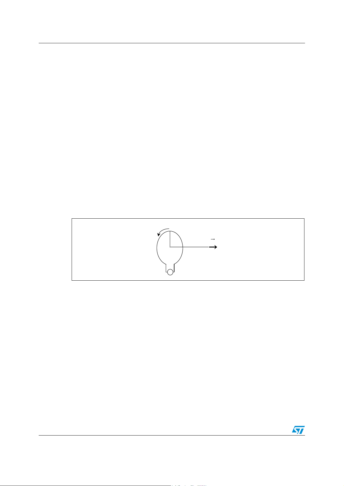
To generate an electromagnetic field, we can assume a circular loop antenna (Figure 2.)
by the tuning circuit.
R
and the tag antenna LT.
R
Figure 2. Circular Loop Antenna
I
r
R
x
~
The Electromagnetic field is given by Equation 1.
Equation 1
IRNR× r
Hrx()
-------------------------------------------------=
2x2
2r
×
R
Where:
● I
is the current in the loop antenna
R
● N
● r
● H
is the number of turns of the loop antenna
R
is the coil radius
R
(x) is measured in A/m
r
H
2
×
R
32⁄
+()
AI09013
8/37
Page 9
AN1806 - APPLICATION NOTE Basic concepts and fundamental equations
An inductive coupling is possible in the near field, the limit between a near field and a far
field is given by Equation 2.
Equation 2
λ
-------------
x
≤
2 π×
Where:
● λ =c/f
In this application note, we use only Tags with a working frequency of 13.56MHz. So, the
limit between a near field and a far field is:
● x ≤ 3.52m
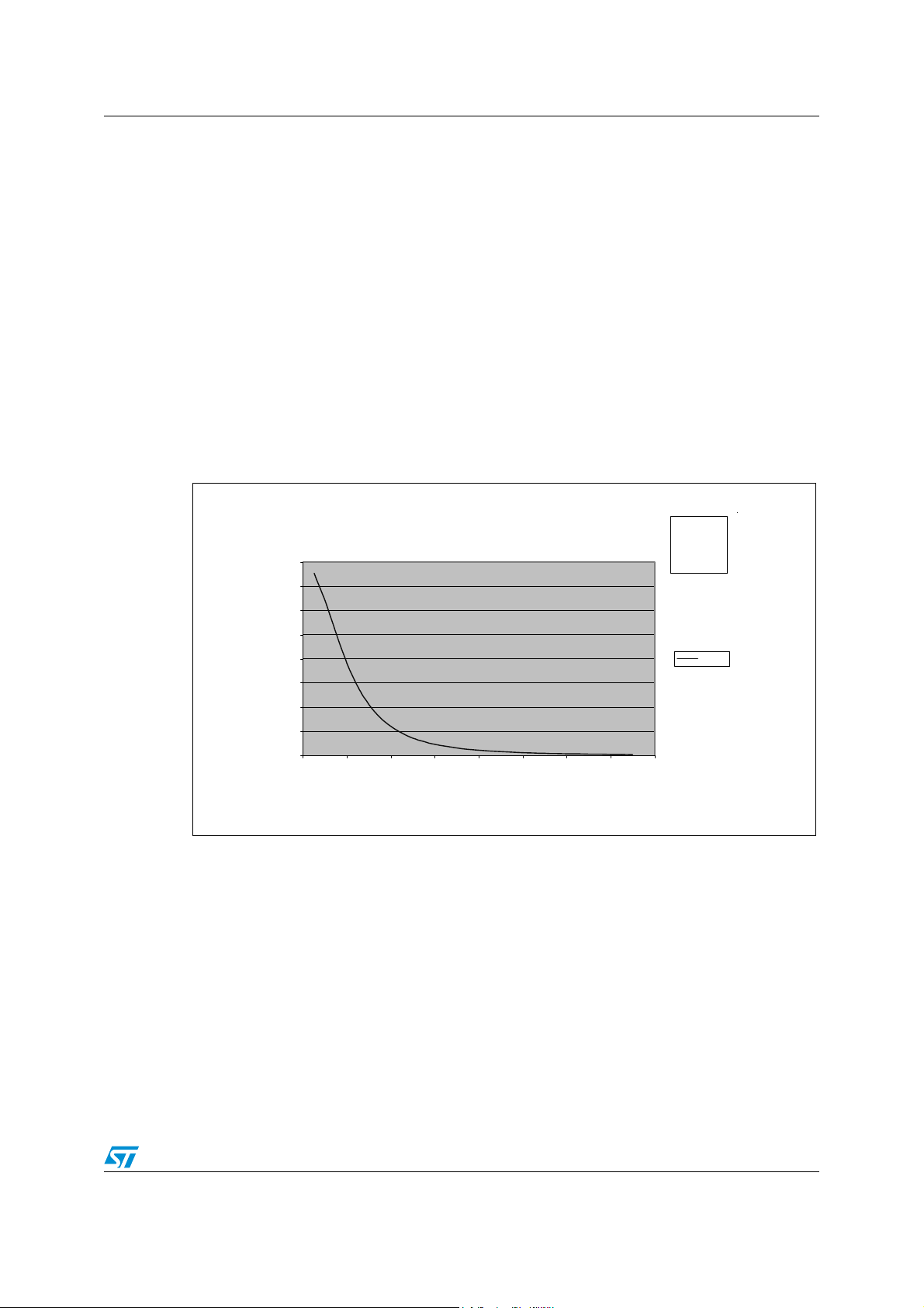
Figure 3 illustrates the magnetic field as a function of the distance of the tag from the reader,
for giv en values of the number of turns, N, the current, I, and the antenna radius, r.
Figure 3. Magnetic Field as a Function of the Distance of the Tag from the Reader
H ( x )
8
7
6
5
4
H [A/m]
3
2
1
0
0 0,02 0,04 0,06 0,08 0,1 0,12 0,14 0,16
Distance [m]
With:
r=2cm
N=2
I=0.2A
H ( x )
AI09022
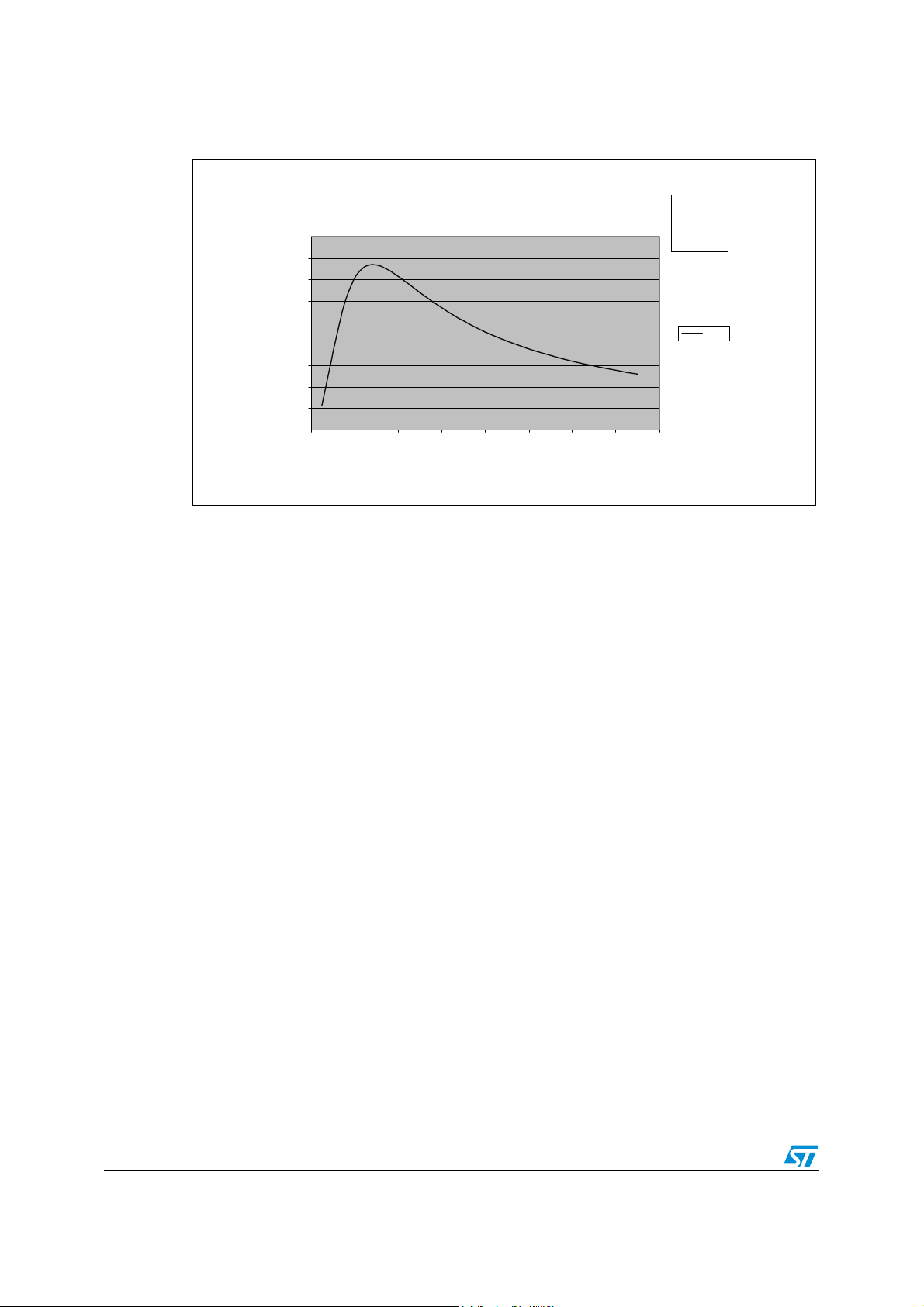
Figure 4 illustrates the magnetic field as a function of the antenna radius, r, for given values
of the number of turns, N, the current, I, of reader antenna, and the distance between tag
and antenna reader, x.
9/37
Page 10
Basic concepts and fundamental equations AN1806 - APPLICATION NOTE
Figure 4. Magnetic Field as a Function of the Antenna Radius
H( r )
4,5
4
3,5
3
2,5
2
H [A/m]
1,5
1
0,5
0
0 0,02 0,04 0,06 0,08 0,1 0,12 0,14 0,16
radius r[m]
In this example we can see that the field decrease when the radius goes beyond an op ti mal
value.
3.2 Inductance, L, and the Antenna
To tune the reader antenna, we need to be able to calculate its inductance.
With:
x=2cm
N=2
I=0.2A
H( r )
AI09023
Equation 3: Inductance of a Circular Loop
L µ0N
× r×
Where:
● r is the mean coil radius
● r
is the wire diameter
0
● N is the number of turns
● µ
● L is measured in H
= 4π10-7H/m
0
1.9
ln×=
r
-----
r
0
10/37
Page 11
AN1806 - APPLICATION NOTE Basic concepts and fundamental equations
Figure 5. Round Planar Spiral Coils
d
AI09024
Equation 4: Inductance of Round Planar Spirals
d
L 31.33 µ0× N2×
------------------------------------ -
×=
8d⋅ 11 c⋅+
Where:
● d is the mean coil diameter
● c is the thickness of the winding
● N is the number of turns
● µ
● L is measured in H
= 4π10-7H/m
0
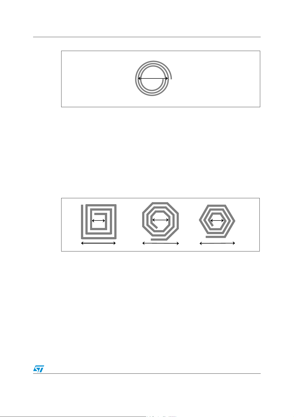
Figure 6. Planar Square, Hexagonal and Octagonal Spiral Coils
d
d
in
d
out
in
d
out
d
in
d
out
Equation 5: Inductance of Planar Square, Hexagonal and Octagonal Coil
LK1µ0× N2×
×=
1K2ρ⋅+
d
--------------------------- -
Where:
● d is the mean coil diameter: (d
–d
is the outer diameter
out
–d
is the inner diameter
in
●
● K
ρ = (d
and K2 depend on the layout (as summarized in Table 1.)
1
out–din
)/(d
out+din
)
out+din
)/2
AI09025
11/37
Page 12

Basic concepts and fundamental equations AN1806 - APPLICATION NOTE
Table 1. K
and K2 values according to layout
1
Layout K
Square 2.34 2.75
Hexagonal 2.33 3.82
Octagonal 2.25 3.55
1
K
2
3.3 Inductance of a Planar Rectangular Coil
We have developed a convenient software tool, using the Grover method (Equation 6) for
calculating the inductance of rectangular planar antenna. The user interface is shown in
Figure 7.
We have found that the software gives a good approximation of the inductance L, in
comparison to measurements of the inductance of a real antenna on an impedance meter.
Equation 6: Grov er Method
LL0M
+=
∑
Where:
● M is the mutual inductance between each of the segments of the antenna
● L
is as defined in Equation 7
0
Equation 7
s
L
=
0
∑
L
j
j1=
Where:
● s is the number of segments
● L
is the self inductance of each segment
j
12/37
Page 13

AN1806 - APPLICATION NOTE Basic concepts and fundamental equations
Figure 7. User Interface Screen of the Planar Rectangular Coil Inductance
Calculator
3.4 Magnetic Coupling Factor
To have a good model of the system, we need to calculate the mutual inductance and
coupling factor of the system.
Equation 8: Magnetic Flux
Where:
● B is the magnetic induction
● dS is the surface cross by the magnetic induction
Equation 9
Φ BS×αcos×=
If α = 0:
● Φ = B.S
Φ BdS
=
∫
°
S
13/37
Page 14

Basic concepts and fundamental equations AN1806 - APPLICATION NOTE
Equation 10: Mutual Inductance between Reader and Tag Antenna
NTΦR×
M
-----------------------=
I
R
Equation 11
2
µ0r
×
Mx()
-------------------------------------------------
2r
×
R
2x2
R
32⁄
+()
STNR× NT××=
Where:
● N
● N
● S
● r
● x is the distance between the reader antenna and the tag antenna
is the number of turns on the reader antenna
R
is the number of turns on the tag antenna
T
is the area of the tag antenna
T
is the coil radius of the reader antenna
R
Equation 12: Magnetic Coupling Factor between Reader and Tag Antenna
Where:
● L
● L
is the inductance of reader antenna
R
is the inductance of tag antenna
T
Therefore:
Equation 13
kx()
kx()
------------------------- -=
Mx()
LTLR×
2
×
µ0r
-------------------------------------------------
2r
×
R
2x2
R
32⁄
+()
STNR× NT×
-------------------------------------- -
×=
LTLR×
14/37
Page 15

AN1806 - APPLICATION NOTE Antenna
4 Antenna
The quality factor is a characteristic of the antenna performance. This parameter is used
when tuning the reader antenna.
Equation 14: Quality Factor
2 π× f0× LR×
---------------------------------------- -=
R
r
LR
Where:
● L
● r
● R
● f
is the inductance of reader antenna
R
is the resistance of reader antenna
LR
is the natural resistance of the reader antenna
LR
is the resonance frequency
0
Q
4.1 Matching Circuit
To tune an antenna at the specific frequency, we performed the following analysis.
First, we started with the equivalent circuit for the antenna system on the board.
Figure 8. Real Circuit for the Antenna System on the Board
Where:
● C
● R
● L is the inductance value of the loop antenna
● R
Then we made use of the following series-to-parallel circuit equivalence.
and C2 are calculated later
1
is the natural resistance of the loop antenna
L
is an additional resistor to have the good value of antenna parameters.
a
C
1
R
a
R
Z
C
2
L
L
AI09027
15/37
Page 16

Antenna AN1806 - APPLICATION NOTE
Figure 9. Series-to-Parallel Circuit Equivalence
R
S
R
P
X
S
X
P
ai08464
Where:
2
X
R
P
S
-----------=
R
S
and:
X
XS=
P
If we assume that:
R
<< X
S
2
S
This gives a new equivalent circuit, as shown in Figure 10.
Figure 10. Parallel Equivalent Circuit
C
1
Z
C
2
Z
eq
Where:
R
-------------------------=
P
RaRL+
L ω0×()
2
L
R
P
ai08466
16/37
Page 17

AN1806 - APPLICATION NOTE Antenna
Figure 11. Equivalent Impedance (Z) Plotted against Frequency (f)
Impedance (Z)
4.000000000K
3.000000000K
2.000000000K
1.000000000K
(1)
ω
1
0
5.9MHz 10MHz 30MHz
1. See resonance frequency in Table 2.
Table 2. Main Results
Resonance frequency Equivalent impedance of the circuit
ω
----------------------------------= ℜ Z[]
0
LC1C2+()
ω
1
Table 3. Values of Capacit o rs
------------------------------------ -=
C
1
(1)
ω
0
1
1
---------------=
LC
2
C1 C2
1
ZRp⋅ω
×
0
------------------------------------------------------------=
2Rp2
C
1
ℜ Z[] Rp=
C
2
RpL C1C+
()
1
--------- - C1–=
Lω
LC1C+
()+
2
0
2
2
Frequency (f)
ai08484
17/37
Page 18

Antenna AN1806 - APPLICATION NOTE
4.2 Current Calculation
To calculate the current, we use the complete system with tuning circuit and the infl uence of
the tag when it is near the reader antenna. F or this , w e need to kno w the m utual inducta nce
between the reader antenna and the Tag.
Figure 12. Coupling between One Tag and One Reader Antenna
Equation 15
Z
r
R
1
V
r
Z
R
I
L
L
M
r
L
t
RjLRω+=
Z
T
RTjLTω
1
----------- -
jLTω
RTjLTω
+=++=
Z
r
I
t
C
t
R
t
1
-----------–
CTω
ai08485
Equation 16
V
R
0ZTjMωI
Equation 17
V
R
18/37
ZRIR⋅ jMωI
+=
Z
R
R
M2ω
-------------- -+
Z
T
+=
R
2
IR⋅=
Page 19

AN1806 - APPLICATION NOTE Antenna
Equation 18
VRZT⋅
--------------------------------------------=
I
R
ZTZR⋅ M2ω
2
+
This equation allows the current I
4.3 VR Calculation
Figure 13. Equivalent Circuits
C
1
C
2
0
Equation 19
in reader antenna to be calculated.
R
C
1
Z
R
a
L
V
R
L
L
e
C
2
V
r
R
V
e
0
1
ai08486
V
r
Z
2
RRaRL+=
Equation 20
Equation 21
V
----------------------------------------------------------------------------------------------------- -
R
4.4 Current Calculation
Combining Equation 18 and Equation 21 we get Equation 22.
RjLω+()jC1ω jRC2ω LC2ω21+–+⋅
V
--------------------- -=
R
Z1Z2+
RjLω+()jC1ω⋅
Ve×=
19/37
VeZ2×
Page 20

Antenna AN1806 - APPLICATION NOTE
Equation 22
------------------------------------------------------------------------------------- -
jRC1ω LC1ω
jR C1C2+()ωLC1C2+()ω– 1+
------------------------------------------------------------------------------------------------------------------------------------------------- -
I
R
R
1LTCTω
------------------------------- -+
T
–
–
2
2
jCTω
R
×
T
RjLRω+()M2ω
+×
1LTCTω
–
------------------------------- -+
jCTω
2
Ve×=
2
20/37
Page 21

AN1806 - APPLICATION NOTE Designing an RFID application
5 Designing an RFID application
It is not easy to calculate directly the optimal antenna to have specific reading distance.
Here is a suggested method:
● Choose a Tag
● Start with an approximate antenna size
● Calculate the real reading range with these paramet er
● Adjust the antenna size appropriately, to get the desired reading range.
Table 4 summarizes the different steps to calculate the additional components and reading
range.
Table 4. Calculation steps
Step Action Input Parameters Output parameters
1 Choose Tag package A3,A4,A5 H
X
Tag
d
out
Choose reading range and select first
2
reader antenna size
Nr
Wc
Sc
Tc
3
Calculate C1, C
Current in Antenna reader
2
f
tune
Calculate
4
Reading distance min/max
Coupling coefficient
● N
● W
● L
● R
● f
● C
● R
● I
: Number of turns for the reader antenna
R
: conductor width of reader antenna
C
: Inductance of reader antenna
R
: Resistance of reader antenna
L
: Tuning frequency of reader antenna
tune
, C2: Tuning capacitance
1
: Additional resistance of reader antenna
a
: Current in reader antenna
r
min
LR[H]
R
C
C
X
max
X
min
[A/m]
[Ω]
L
ra[Ω]
[F]
1
[F]
2
Ir [A]
[m]
K
min
[m]
21/37
Page 22

Designing an RFID application AN1806 - APPLICATION NOTE
5.1 Using the Excel Spreadsheet
Before using the Excel spreadsheet, you must to configure it:
● In Tools menu, click on sub menu Add-Ins
● Select the Analysis ToolPak check box, then click OK
Figure 14. Excel Configuration
5.2 Step 1
Choose the Tag package according to your application:
● A3: size 38mm x 38mm
● A4: size 15mm x 15mm
● A5: size 65mm x 42mm
If you have no constrains on the size tag, select the maximum size (A5) to start.
22/37
Page 23

AN1806 - APPLICATION NOTE Designing an RFID application
5.3 Step 2
Choose reading distance and select first size antenna reader.
Select the diameter d
● d
out
●
Nr=2
● W
● S
● T
● L and R
Table 5. Parameter values
c
=0.0005 [m]
c
function of board specifications (Standard 35x10-6 [m])
c
d
[m] Nr
out
0.055 2 0.002 0.0005 4.77079E-07 0.000035 0.19853714
5.4 Step 3
● Keep the default parameter for the f
● Ra, C1 and C2 are the additional components to tune the reader antenna.
Table 6. Parameter values for tuning
equal to the reading distance you wish. Start with:
out
= X
Tag
=0.002 [m]
are the electrical characteristics of your antenna.
L
WC [m]
(width of
conductor)
SC [m] (space
between
conductor)
(tuning frequency of reader antenna)
tune
L [H]
TC [m]
Thickness of
conductor
RL [ohm]
f
Tunning
tune
Frequency [Hz]
Ra [ohm] C1s [pF] C2p [pF]
1.42E+07 0.33353276 1.1089E-10 1.5242E-10
23/37
Page 24

Designing an RFID application AN1806 - APPLICATION NOTE
5.5 Step 4
The last table gives three pieces of information (the green background, no t shown in
Table 7, indicates those values that are OK, and the red background, shown shaded in
Table 7, indicates those that are not OK):
● The self supply distance available
● The coupling coefficient between rea der and Tag available for each reading distance.
● The magnetic field value for each reading distance.
Table 7. Computed read range as a function of K and the H field
Distance Between Tag and
Reader [m]
0 0.29747676 4.09952789
0.005 0.28079988 4.07239802
0.01 0.23907764 3.92851237
0.015 0.18903897 3.57250903
0.02 0.14328997 3.02781035
0.025 0.10674754 2.42659743
0.03 0.07943063 1.88468486
0.035 0.05957594 1.44786262
0.04 0.0452454 1.11426535
0.045 0.0348568 0.86480968
0.05 0.02724888 0.67892022
0.055 0.02160527 0.53964094
0.06 0.01736053 0.43426455
0.065 0.0141234 0.35361388
0.07 0.01162142 0.29113953
0.075 0.00966294 0.24216658
K H(x) [A/m]
0.08 0.00811155 0.20333723
0.085 0.00686896 0.1722174
0.09 0.00586343 0.14702389
0.095 0.00504195 0.12643577
In this example the maximum reading distance is 4.5cm.
24/37
Page 25

AN1806 - APPLICATION NOTE Designing an RFID application
Figure 15. Basic Schematic
ANT2
R8
C5
100pF50V
0R
10pF50V
8pF50V
C8’
C7’
33pF50V
C7
120pF50V
D1
1N4148 (OPT IONAL)
C8
R7
0R
X1
C1 7pF50V
VCC
C6
100nF50V
U1
WURTH 742-792-042
C3
OPT
13.56MHz
9
12
13
14
OSC1
GND_RF
22nF50V
11
GND
OSC2
E2
10
SCL
8
0R
16
15
VCC
RF OUT
Vref1RF IN2E03E14E25GND_RF6GND7GND
FL7
R5
C2 7pF50V
SDA
R6
CRX14
SCL
SDA
C4
22uF 10V
+
VCC
0R
0R
FL5
J1
0R
FL4
FL6
123
4
R3
OPT
R1
OPT ANT1
VCC
R4
0R
E1
R2
0R
E0
ai08488B
25/37
Page 26

Calculation details of serial-to-Parallel Conversion AN1806 - APPLICATION NOTE
Appendix A Calculation details of serial-to-Parallel
Conversion
The two circuits in Figure 9 are equivalent, where:
+
R
S
<< X
S
2
X
S
RPRS×
----------------------- -=
jRPXP×
-------------------------=
RPjXP+
X
S
2
S
2
X
S
--------+==
S
R
S
RSjXS+
Multiplying by the complex conjugate we find:
2
R
S
---------------------- - R
X
P
R
and:
If:
R
P
this simplifies to:
2
X
P
1
P
--------------------- -=
RaRL+
S
-----------=
R
S
XS=
2
Lω0()
from C2, L and RP in parallel:
eq
1
------- - jC2ω++=
jLω
∗
R
jLω
P
∗
jLω++
P
R
P
and:
X
This gives the equivale nt circuit shown in Figure 10, whose impedance (Z) versus frequency
(f) is plotted in Figure 11, where:
R
P
We start to calculate the equivalent impedance Z
1
and so:
----------
Z
Z
eq
--------
R
eq
------------------------------------------------------------------=
jLω RPjC2ω∗R
26/37
Page 27

AN1806 - APPLICATION NOTE Calculation details of serial-to-Parallel Conversion
We can also calculate the equivalent impedance Z:
Z
1
Z
------------
jC1ω
--------------------------------------------------------------------------------------- -=
Z
jC1ω∗RPLC2RPω
------------------------------------------------------------------+=
jLω RPjC2ω∗R
+
jLω R
P
The first resonant frequency occurs when:
1LC1C2+()
– 0=
We define ω = ω
to be at this point, and hence that:
0
ω
0
1
------------ Zeq+=
jC1ω
∗
R
jLω
P
∗
jLω++
P
∗
1LC1C2+()
–
–
----------------------------------=
2
2
∗
ω
1
∗
C1Lω
–
2
ω
2
LC1C2+()
We find the equivalent impedance, Z, at this frequency, ω
jLω
Z
-------------------------------------------------------------------------------------------------- -=
∗
jC1ω
Z
------------------------------------------------------------------------------------------------ -=
j∗C1RPLC1C2RPω
RPLC2RPω
0
–
–
0
2
0
jL
2
0
We can separate the real and imaginary parts:
Z
C1RPLL2C1C2Rω
---------------------------------------------------------------------------------------------- - j
C1RPLC1C2RPω
– C1Lω
–
0
Taking the real part, and substituting for ω
2
0
2
()
+
0
we obtain:
0
2
C1RPLC1C2Rω
----------------------------------------------------------------------------------------------- -
⋅–=
RPLC1C2+()
ℜ Z[]
---------------------------------------------------------=
2
2
C
R
1
LC1C2+()+
P
:
0
C1Lω
–
–
C1Lω
–
2
0
0
C1L2ω
0
2
2
C1Lω
()
+
0
2
0
27/37
Page 28

Calculation details of serial-to-Parallel Conversion AN1806 - APPLICATION NOTE
5.6 Calculation of the Impedance of Equivalent Circuit at the Second Resonance Frequency
We start with the expression of the equivalent impedance Z, calculated earlier:
jLω R
Z
---------------------------------------------------------------------------------------=
jC1ω∗RPLC2RPω
∗
+
1LC1C2+()
P
–()C1Lω
The second resonant frequency occurs when:
RPLC2RPω
– 0=
–
2
2
2
∗
ω
–
2
We define ω = ω
We find the equivalent impedance, Z, at this frequency, ω
to be at this point, and hence that:
1
ω
---------------=
1
LC
∗
1LC1C2+()
+
–
P
Z
jLω1R
-----------------------------------------------------------------------------------------–=
C1Lω
1
2
:
1
2
∗
ω
1
2
1
We can separate the real and imaginary parts, and take the real part:
2
∗
ω
1
Substituting for ω
we obtain:
1
ℜ Z[]
∗
R
1LC1C2+()
–
P
-----------------------------------------------------------------------–=
C1Lω
2
1
ℜ Z[] RP=
Table 8. Summary of the Main Results
Resonance frequency Equivalent impedance of the circuit
ω
0
ω
1
28/37
1
----------------------------------=
LC1C2+()
1
---------------=
LC
2
ℜ Z[]
RpL C1C+
------------------------------------------------------------=
2Rp2
C
1
ℜ Z[] Rp=
()
LC1C+
()+
2
2
Page 29

AN1806 - APPLICATION NOTE Calculation details of serial-to-Parallel Conversion
Now we can easily calculate the value of the C1 and C2 capacitors, in terms of Z, Rp, L, ω0:
ω
0
We can substitute for ω
1
----------------------------- -= LC1ω
LC1C2+
:
0
and:
C
2
Table 9. Values of the Capaci tors
C1 C2
1
------------------------------------ -=
C
1
ZRp⋅ω
×
0
2
+ 1= C
LC2ω
0
RPZ–
C
------------------ -=
1
R
2
2
R
ω
ZRPZ––
P
0
--------------------------------------------------- -=
2
Lω
0
2
0
2
2
ω
Z
P
0
2
2
R
ω
Z
P
0
1
--------- - C1–=⇒⇒
2
2
Lω
0
1
--------- - C1–=
C
2
Lω
2
0
29/37
Page 30

Calculation Details of Current Calculation AN1806 - APPLICATION NOTE
Appendix B Calculation Details of Current Calculation
To calculate the current, we use the complete system with tuning circuit and the infl uence of
the tag when it is near the reader antenna.
For this, we need to know the mutual inductance between the reader antenna and the Tag.
Figure 16. Coupling factor model
Equation 23
Z
r
R
1
V
r
Z
R
I
L
L
M
r
L
t
RjLRω+=
Z
T
RTjLTω
1
----------- -
jLTω
RTjLTω
+=++=
Z
r
I
t
C
t
R
t
1
-----------–
CTω
ai08485
Equation 24
V
R
0ZTjMωI
Equation 25
V
R
Equation 26: To calculate the Current, I
I
R
30/37
ZRIR⋅ jMωI
+=
Z
R
in Reader Antenna
R
R
M2ω
-------------- -+
Z
T
+=
R
2
IR⋅=
VRZT⋅
--------------------------------------------=
ZTZR⋅ M2ω
2
+
Page 31

AN1806 - APPLICATION NOTE Calculation Details of Current Calcul ation
5.7 VR Calculation
Figure 17. Equivalent circuits
C
1
C
1
Z
R
a
L
V
R
L
C
2
e
C
2
V
r
V
e
1
Z
2
V
r
Note:
L
0
0
R
ai08486
RRaRL+=
VeZ2×
V
--------------------- -=
R
Z1Z2+
RjLω+()jC1ω⋅
V
----------------------------------------------------------------------------------------------------- -
R
RjLω+()jC1ω jRC2ω LC2ω21+–+⋅
Z
1
------------=
1
jC1ω
Ve×=
Z
2
RjLω+
---------------------------------------------------=
jRC2ω LC2ω21+–
RjLω+
---------------------------------------------------
jRC2ω LC2ω
-----------------------------------------------------------------------
V
R
---------------------------------------------------
jRC2ω LC2ω
– 1+
RjLω+
– 1+
31/37
2
Ve×=
1
2
------------+
jC1ω
Page 32

Calculation Details of Current Calculation AN1806 - APPLICATION NOTE
RjLω+
---------------------------------------------------
V
R
jRC2ω LC2ω
– 1+
V
R
----------------------------------------------------------------------------------------------------- -
5.8 Current Calculation
------------------------------------------------------------------------------------- jR C1C2+()ωLC1C2+()ω– 1+
------------------------------------------------------------------------------------------------------------------------------------------------- -
I
R
jRC1ω LC1ω
R
T
2
RjLω+()jC1ω jRC2ω LC2ω21+–+⋅
–
1LTCTω
–
------------------------------- -+
jCTω
jRC2ω LC2ω
----------------------------------------------------------------------------------------------------- -
– 1+
RjLω+()jC1ω jRC2ω LC2ω
2
jC1ω⋅
– 1++⋅
2
RjLω+()jC1ω⋅
Ve×=
2
1LTCTω
R
×
–
------------------------------- -+
T
jCTω
2
Ve×=
2
RjLRω+()M2ω
2
+×
Ve××=
32/37
Page 33

AN1806 - APPLICATION NOTE Demo kit board
Appendix C Demo kit board
Figure 18. Layout of Demo-kit Board
ai08489
33/37
Page 34

Demo kit board AN1806 - APPLICATION NOTE
Figure 19. Component Implementation
ai08490
Table 10. Bill of Materials
Designators Value Footprint Comment
R7 0R 0603 ±1%, 0.1W
R8 0R 0603 ±1%, 0.1W
R2 0R 0603 ±1%, 0.1W
R4 0R 0603 ±1%, 0.1W
R6 0R 0603 ±1%, 0.1W
FL4 0R 0805 ±1%, 0.1W
FL5 0R 0805 ±1%, 0.1W
FL6 0R 0805 ±1%, 0.1W
C6 100nF 0603 ±5%, 50V
C8 100p 0603 ±5%, 50V
C7 120p 0603 ±5%, 50V
X1 13.56MHz XTALCMS
C7' 33p 0603 ±5%, 50V
D1 1N4148 1210 Option
C3 20nF 0603 ±5%, 50V
C4 22uF 1210 Tantalum ±10%, 6.3V
C5 10p 0603 ±5%, 50V
C1 7pF 0603 ±5%, 50V
C2 7pF 0603 ±5%, 50V
C8' 8p 0603 ±5%, 50V
J1 Connector HE14_4H
U1 CRX14 SO16 ST
FL7 Ferrite 0805 Wurth 742-792-042
34/37
Page 35

AN1806 - APPLICATION NOTE Demo kit board
Table 10. Bill of Materials
Designators Value Footprint Comment
R1 OPT 0603
R3 OPT 0603
R5 OPT 0603
35/37
Page 36

Revision history AN1806 - APPLICATION NOTE
6 Revision history
Table 11. Document Revision History
Date Version Revision Details
10-Dec-2003 1.0 First Issue.
Document moved to new template. Equations 4 and 5 corrected.
Titles added to Appendix C, Figure 17, Table 1, Table 4, Table 5,
06-Dec-2005 2.0
13-Feb-2006 3.0 CRX14 pinout modified in Figure 15: Basic Schematic.
Table 6 and Table 7. Title of Figure 16: Coupling factor model
modified.
and ω2 and note added to Figure 12: Coupling between One
ω
1
Tag and One Reader Antenna.
36/37
Page 37

AN1806 - APPLICATION NOTE
Please Read Carefully:
Information in this document is provided solely in connection with ST products. STMicroelectronics NV and its subsidiaries (“ST”) reserve the
right to make changes, corrections, modifications or improvements, to this document, and the products and services described herein at any
time, without notice.
All ST products are sold pursuant to ST’s terms and conditions of sale.
Purchasers are solely res ponsibl e fo r the c hoic e, se lecti on an d use o f the S T prod ucts and s ervi ces d escr ibed he rein , and ST as sumes no
liability whatsoever relati ng to the choice, selection or use o f the ST products and services described herein.
No license, express or implied, by estoppel or otherwise, to any intellectual property rights is granted under this document. If any part of this
document refers to any third pa rty p ro duc ts or se rv ices it sh all n ot be deem ed a lice ns e gr ant by ST fo r t he use of su ch thi r d party products
or services, or any intellectua l property c ontained the rein or consi dered as a warr anty coverin g the use in any manner whats oever of suc h
third party products or servi ces or any intellectual property contained therein.
UNLESS OTHERWISE SET FORTH IN ST’S TERMS AND CONDITIONS OF SALE ST DISCLAIMS ANY EXPRESS OR IMPLIED
WARRANTY WITH RESPECT TO THE USE AND/OR SALE OF ST PRODUCTS INCLUDING WITHOUT LIMITATION IMPLIED
WARRANTIES OF MERCHANTABILITY, FITNESS FOR A PARTICUL AR PURPOS E (AND THEIR EQUIVALE NTS UNDER THE LAWS
OF ANY JURISDICTION), OR INFRINGEMENT OF ANY PATENT, COPYRIGHT OR OTHER INTELLECTUAL PROPERTY RIGHT.
UNLESS EXPRESSLY APPROVED IN WRITING BY AN AUTHORIZE REPRESENTATIVE OF ST, ST PRODUCTS ARE NOT DESIGNED,
AUTHORIZED OR WARRANTED FOR USE IN MILITARY, AIR CRAFT, SPACE, LIFE SAVING, OR LIFE SUSTAINING APPLICATIONS,
NOR IN PRODUCTS OR SYSTEMS, WHERE FAILURE OR MALFUNCTION MAY RESULT IN PERSONAL INJURY, DEATH, OR
SEVERE PROPERTY OR ENVIRONMENTAL DAMAGE.
Resale of ST products with provisions different from the statements and/or technical features set forth in this document shall immediately void
any warranty granted by ST fo r the ST pro duct or serv ice describe d herein and shall not cr eate or exten d in any manne r whatsoever , any
liability of ST.
ST and the ST logo are trademarks or registered trademarks of ST in various countries.
Information in this document su persedes and replaces all information previously supplied.
The ST logo is a registered trademark of STMicroelectronics. All other names are the property of their respective owners.
© 2006 STMicroelectronics - All rights reserved
STMicroelectronics group of compan ie s
Australia - Belgium - Brazil - Canada - China - Czech Republic - Finland - France - Germany - Hong Kong - India - Israel - Italy - Japan -
Malaysia - Malta - Morocco - Singapore - Spain - Sweden - Switzerland - United Kingdom - United States of America
www.st.com
37/37
 Loading...