

Page 1

AN1798
Application note
How to use the STR71x A/D converter
and apply a conversion speed-up technique
Introduction
This application note describes how to use the Sigma-Delta Analog to Digital Converter
(ADC) in the STR71x microcontroller.
It describes the Sigma-Delta ADC calibration and linearization technique and shows how to
apply a conversion speed-up technique to reduce the conversion time.
November 2007 Rev 3 1/16
www.st.com
Page 2

Contents AN1798
Contents
1 Principle of operation . . . . . . . . . . . . . . . . . . . . . . . . . . . . . . . . . . . . . . . . 3
2 STR71x ADC features . . . . . . . . . . . . . . . . . . . . . . . . . . . . . . . . . . . . . . . . 4
2.1 Clock timing . . . . . . . . . . . . . . . . . . . . . . . . . . . . . . . . . . . . . . . . . . . . . . . . 4
2.2 ADC output, Gain and offset features . . . . . . . . . . . . . . . . . . . . . . . . . . . . 5
2.3 Round-Robin and Single channel modes . . . . . . . . . . . . . . . . . . . . . . . . . . 5
2.4 Conversion data availability and interrupt generation . . . . . . . . . . . . . . . . . 5
3 Calibration and linearization technique . . . . . . . . . . . . . . . . . . . . . . . . . 7
3.1 Principle . . . . . . . . . . . . . . . . . . . . . . . . . . . . . . . . . . . . . . . . . . . . . . . . . . . 7
3.2 Hardware implementation . . . . . . . . . . . . . . . . . . . . . . . . . . . . . . . . . . . . . 8
3.3 Firmware description . . . . . . . . . . . . . . . . . . . . . . . . . . . . . . . . . . . . . . . . . 9
4 STR71x ADC conversion speed-up . . . . . . . . . . . . . . . . . . . . . . . . . . . . 12
4.1 Hardware implementation . . . . . . . . . . . . . . . . . . . . . . . . . . . . . . . . . . . . 12
4.2 Firmware description . . . . . . . . . . . . . . . . . . . . . . . . . . . . . . . . . . . . . . . . 12
5 Revision history . . . . . . . . . . . . . . . . . . . . . . . . . . . . . . . . . . . . . . . . . . . 15
2/16
Page 3

AN1798 Principle of operation
1 Principle of operation
Sigma-Delta converters, known also as oversampling converters, sample the input signal
many times for each output sample with a frequency rate much greater than the Nyquist
frequency (twice the input bandwidth). A Sigma-Delta converter consists of two blocks, the
first is the Sigma-Delta modulator which produces the bit stream to the second part which
consists of a digital filter and decimator.
Figure 1. A Sigma-Delta converter block diagram
Integrator
Vin
+
Σ
ADC
N bits of DATA
Digital filter
and Decimator
-
N bits
DAC
N bits
The STR71x ADC is a Sigma-Delta converter which composed of a second-order SigmaDelta modulator followed by a sinc3 digital filter and decimator.
3/16
Page 4
STR71x ADC features AN1798
2 STR71x ADC features
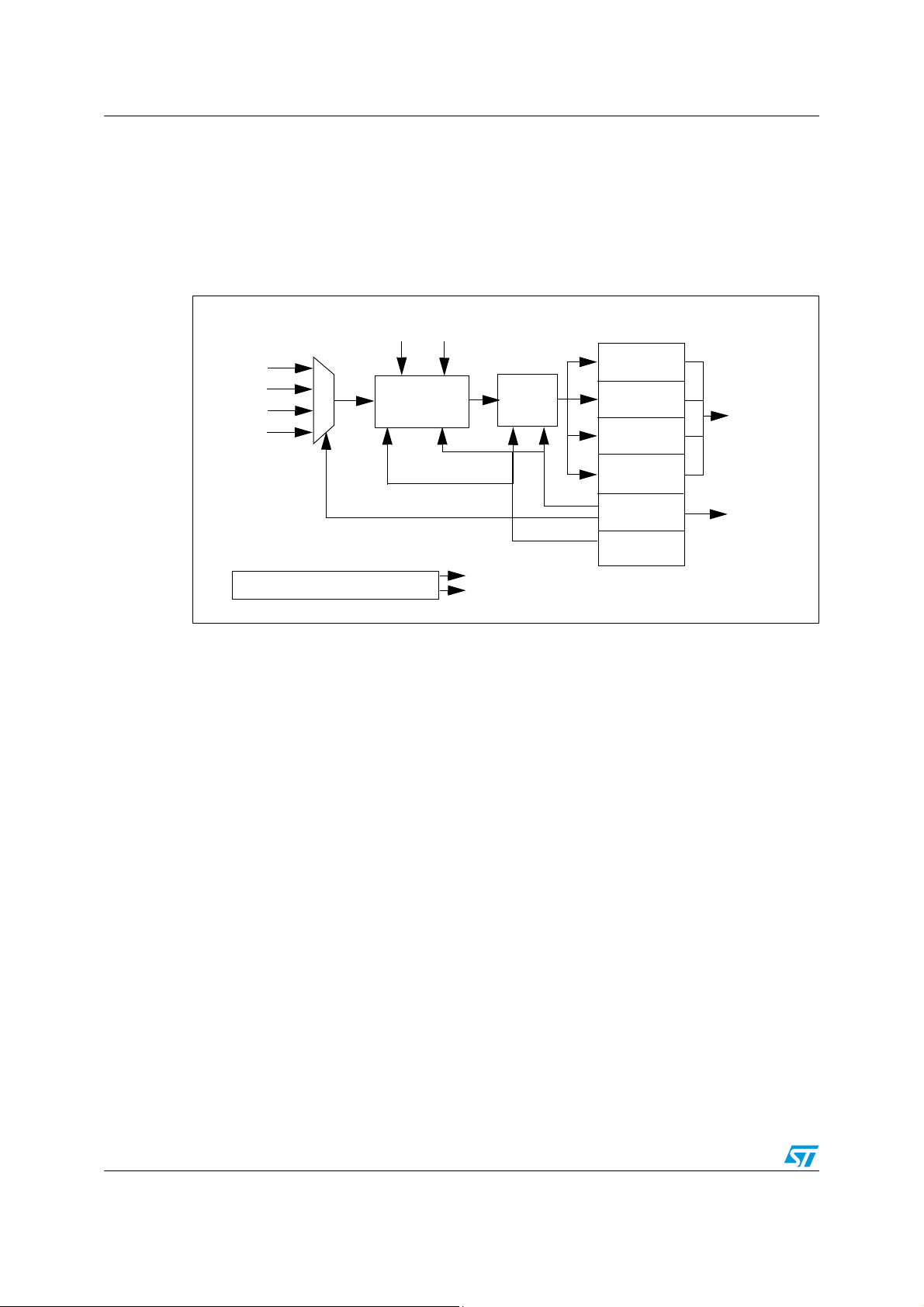
The STR71x ADC consists of four channels (Ip1 to Ip4 or AIN0 to AIN3) to convert signals
with an input range of 0 to 2.5 V into 12-bit format. The following figure shows the ADC
module of STR71x.
Figure 2. ADC STR71x block diagram
Ip1
Ip2
Ip3
Ip4
Bandgap Voltage Reference
2.1 Clock timing
Each channel supports up to 1 kHz for sampling frequency (fs), consequently the signal
frequency can not exceed 500 Hz (to respect the
f
(oversampling frequency) is the clock frequency which clocks the Sigma-Delta
Mod
modulator. This frequency can not exceed 2.1 MHz and therefore the maximum sampling
frequency is equal to 1 kHz (fs = 2.1 MHz / 512 * 4 = 1 kHz).
VCM VRef
Σ∆
Modulator
fs = f
Mod
Sinc3
Filter
VCM
VRef
/ 512 * 4
Registers
Ch0 Data
Ch1 Data
Ch2 Data
Ch3 Data
Control/
Status
Prescaler
Output
Data
Bus
IRQ
Nyquist frequency condition).
f
is generated by PCLK2 and divided down by the prescaler factors configured in the
Mod
ADC_CPR register. The prescaler output frequency must be not greater than 2.1 MHz.
f
= f
Mod
Example: if f
f
= fs * 512 * 4 = 1 kHz * 512 * 4 ~ 2 MHz
Mod
The Prescaling factor = f
= 16 MHz and the desired sampling frequency fs= 1 kHz.
PCLK2
PCLK2
PCLK2
/ f
= 16 MHz / 2 MHz = 8
Mod
This value being twice the prescaler register value: so, the value to be configured in the
ADC_CPR register is equal to 0x4. (see STR71x Reference Manual, ADC section: ADC
prescaler setting table)
4/16
/ Prescaling factor
Page 5
AN1798 STR71x ADC features
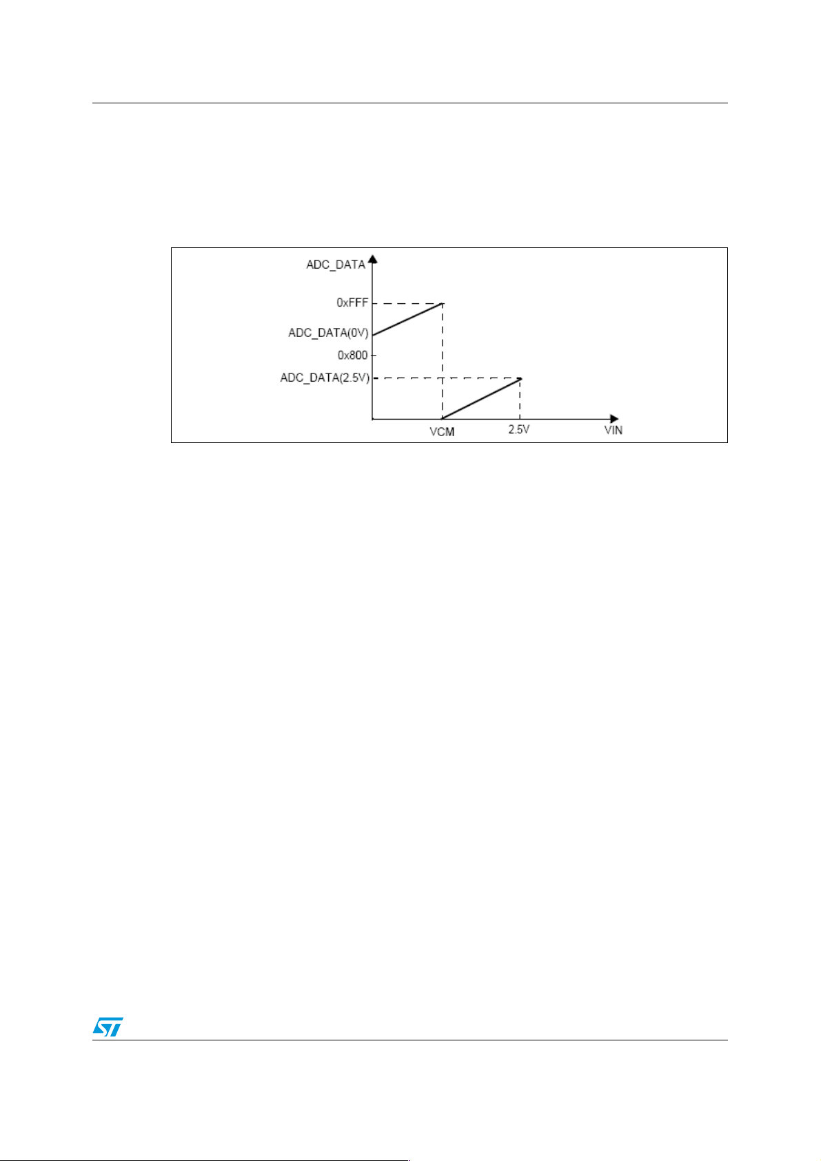
2.2 ADC output, Gain and offset features
The converted values stored in ADC_DATA[n] 16-bit register are signed two’s complement
values and only the 12 most significant bits are used.
The following figure gives the ADC output versus the input voltage.
Figure 3. ADC output
ADC_DATA(0V) and ADC_DATA(2.5V) are the conversion of 0V and 2.5V respectively.
The gain of the ADC is given by:
G = [0xFFF - ADC_DATA(0V) + ADC_DATA(2.5V)] / 2.5
The quantum is calculated by the following equation:
q = 2.5V / [0xFFF - ADC_DATA(0V) + ADC_DATA(2.5V)]
The offset is the digital unsigned value of 0V (ADC_DATA(0V)) and the application should
subtract this offset when reading all the conversion results.
2.3 Round-Robin and Single channel modes
These modes are provided to simplify the use of the ADC.
● Single channel mode selects one channel that is the only channel input to the Sigma-
Delta modulator. To use single channel mode, bit 6 in the ADC_CSR register must be
set to 1. A valid sample in this mode is produced every 2048 modulator clock cycles.
● Round-Robin mode (which is the normal mode) allows you to simplify your software
code and avoid using an endless loop (while (1)) to get the converted values of all
channels continuously. This process is repeated for each of the channels continually in
a round-robin fashion. A valid sample in this mode is produced every 512 modulator
clock cycles for each channel.
2.4 Conversion data availability and interrupt generation
The End of Conversion is indicated by four flags or by interrupt generation. The four flags
are the Data Available flags (DA[n]) in the Control Status register. They allow the application
software to determine which channel data register has a new sample ready to be read. Each
DA[n] flag corresponds to ADC channel n. They are set by hardware as soon as a new
sample on the corresponding channel is available and they are automatically cleared when
the corresponding data register is read.
5/16
Page 6

STR71x ADC features AN1798
The STR71x ADC is able to generate an interrupt at the end of conversion. This interrupt
depends on the conversion mode. In Single Channel mode an interrupt is generated if, in the
CSR register, the interrupt bit and Data Available flag for the selected channel are set. In
Round Robin mode, an interrupt is generated if all interrupt bits and all Data Available flags
in the CSR are set.
6/16
Page 7

AN1798 Calibration and linearization technique
3 Calibration and linearization technique
3.1 Principle
ADC calibration is done by software, it consists of a new calculation of the gain, the quantum
and the offset each time the application is executed.
Initially, the you have to obtain the ADC conversion digital result for 0 V and 2.5 V by
applying two stable voltage external sources (0 V and 2.5 V) to the ADC input in order to
calculate the ADC gain and the quantum.
Next, you need to calculate the average of these two values by reading each value n times
and dividing by n to reach the average values.
After that, calculate the unsigned values of ADC_DATA(2.5V) and ADC_DATA(0V) (these
values are two’s complement).
Then, calculate the ADC range or the sweep of conversion in count / volt:
sweep = Unsigned[ADC_DATA(2.5V)] - Unsigned[ADC_DATA(0V)].
Finally, calculate the gain and the quantum:
G = sweep / 2.5 V
q = 2.5 V / sweep
The principle of linearization is to shift the half-lines ‘A’ and ‘B’ respectively down and up to
obtain one segment: ‘C’. Then, subtract the offset as shown in the following figure.
Figure 4. Linearization
ADC_DATA
0xFFF
ADC_DATA(0V)
0x800
ADC_DATA(2.5V)
Offset
A
C
B
VCM=1.25V
Linearize the segments
2.5 V
then
subtract the
offset
Vin
ADC_DATA
0xFFF
Full scale
0x800
Offset
Offset
Counts off
C
Final segment
VCM=1.25 V
Subtract the offset
2.5 V
Vin
These segments are linearized by software by adding 0x800 if the reading value is positive
(the most significant bit is set to 0). If this value is negative (the most significant bit is set to
1) subtract its two’s complement from 0x800. Then, subtract the offset from this value. The
offset value is equal to Unsigned[ADC_DATA(0V)].
7/16
Page 8

Calibration and linearization technique AN1798
3.2 Hardware implementation
In order to calibrate the ADC, apply two stable voltage sources and read these values to
obtain the dynamic of the ADC.
This can be done by applying the 2.5 V source to one of four ADC channels (for example
AIN1) and connecting the ground to another channel (for example AIN0). Two channels are
reserved for hardware calibration.
It is possible to obtain the 2.5 V source by a zener diode (ex: TS824-2.5) and a dedicated
resistor.
The following figure shows the calibration hardware implementation:
Figure 5. Calibration hardware implementation
3.3 V
AVD D
0.1µF
AGND
STR71x
AIN0
AIN1
I
k
D1(*)
R1
1.6K
3.3 V
two channels for calibration
AIN2
AIN3
two available input channels
(*) D1 ex: TS824-2.5
The resistor value is chosen to have a current I
< 1mA (Reverse break down current).
k
This condition (see TS824-2.5 datasheet) allows to have a V
I
By choosing I
= 500µA < 1mA
k
Afterwards: R1 = (V
= (3.3 - 2.5) / 500 * 10
in
- V
Ref
) / I
k
= (Vin - V
k
-6
Ref
) / R1
= 1.6K
more stable than if Ik >1 mA.
Ref
8/16
Page 9

AN1798 Calibration and linearization technique
3.3 Firmware description
The calibration, the linearization and offset compensation are done by software. As
described in Section 3.1, the ADC conversation range, the gain and the quantum are
computed. Figure 6 shows an example flowchart of the software:
Figure 6. Calibration firmware implementation
Calibration section
Start of calibration
Configure ADC inputs to high
impedance analog inputs
Configure the prescaler
Configure the conversion mode:
Single
Start the conversion
Select ADC Channel 1
Compute the average of the
converted value: 2.5V (ADC_MAX)
Select ADC Channel 0
Compute the average of the
converted value: 0V (ADC_Min)
Compute the unsigned value of
2.5V: Unsigned_MAX
Compute the unsigned value of
0V: Unsigned_Min
Get calibrated conversion results
section
Start of conversion
polling on Channel 3
Select Channel 3
Get the conversion:
Conversion_Result
Compute the unsigned value of
Conversion_Result:
Unsigned_Result
Calibrated_Result_Data =
Unsigned_Result - Unsigned_Min
Calibrated_Result_Volt =
Calibrated_Result_Data * q
Compute the sweep of conversion
sweep = Unsigned_MAX - Unsigned_Min
Compute the quantum q
q = 2.5V/sweep
End of Calibration
Note: The delivered software and
flowcharts are compatible with
the following hardware configuration:
Channel_0 to read the ground value
Channel_1 to read the 2.5 V value
Channel_3 to convert the signal
Please refer to Figure 5.
You can modify the hardware configuration
but then you have to change also
the software to be in line with your hardware.
9/16
Page 10

Calibration and linearization technique AN1798
Figure 7. Compute the unsigned value of a converted value
Begin
Get the converted value from ADC_DATA register
Value > 0?
Yes
No
value=
value+0x800
Return value
End
value=
0x800- [(~value)-1]
Figure 8. Compute the average of the converted value
Begin
i = 0, N: number of times the
channel is converted
i < N?
Yes
value = ADC_value
No
Average = sum/N
sum = sum + value
i++
10/16
Return Average
End
Page 11

AN1798 Calibration and linearization technique
Example of results with this software:
The software determine the averages of the two voltage levels (0 and 2.5 V) which are
applied to Channel 0 and Channel 1 respectively and these results are shown in the
debugger:
ADC_Min: 0x963 (0 V) = 2403 decimal (average value)
ADC_Max: 0x66E (2.5 V) = 1646 decimal (average value)
Then, the software determines their unsigned values:
Unsigned_Min (0 V) = 0x800 - ((~0x963 & 0xFFF) + 1)
= 0x165
= 357 decimal
Unsigned_Max (2.5 V) = 0x800 + 0x66E
= 0xE6E
= 3694 decimal
Then the software determines the sweep of conversion:
Sweep = Unsigned_Max - Unsigned_Min
= 0xE6E - 0x165
= 0xD09
= 3337 decimal
Finally it determines the gain G and the quantum q:
G = 3337 / 2.5 V = 1334.8 Volt
-1
q = 2.5V/3337 = 749 µV
For example a voltage level = 1.60 V is applied to Channel 0, we get:
Conversion_Result = 0x124
Unsigned_Result = 0x800 + 0x124 = 0x924
The calibrated conversion result after subtracting the offset is:
Calibrated_Result_Data = Unsigned_Result - Unsigned_Min
= 0x9C0 - 0x165
= 0x85B
= 2139 decimal
It is possible also to determine the applied voltage value in Channel 0 by multiplying this
result by the quantum:
Calibrated_Result_Volt = 2139 * 749 µV = 1602111µV ~ 1.60 V
Ideally 1.60V converted value is: 1334.8 * 1.60 = 2136
The accuracy of conversion is: 2136 / 2139 = 99.8%
11/16
Page 12

STR71x ADC conversion speed-up AN1798
4 STR71x ADC conversion speed-up
This section gives an example of how to reduce the conversion time of the A/D Converter of
the STR71x microcontroller, when only one input channel needs to be converted. This is
achieved using Round Robin mode instead of Single Channel mode to convert an analog
input signal which must be connected to all four analog input pins of the converter. By
configuring the conversion time to 1ms per channel, the conversion Speed-Up technique
allow conversion time to be reduced down to 250 µs.
4.1 Hardware implementation
In Single Channel mode, a valid sample for the selected channel is produced only every
2048 clock cycles, with the same output frequency as Round Robin mode which samples
the four channels (512 clock cycles for each channel). Consequently, the conversion time for
one analog voltage can be reduced by using Round Robin mode instead of Single Channel
mode.
The four ADC inputs have to be connected to the same analog voltage input in order to use
Round Robin conversion mode. As shown in Figure 9, only one input can be used when this
technique is applied.
Figure 9. Speed-Up hardware implementation
3.3V
0.1µF
AVD D
AGND
STR71x
4.2 Firmware description
To use the procedure described above, the ADC has to be driven in polling mode because in
Round Robin mode, an interrupt is generated only when the four input channels have been
converted and all the Data Available flags in the Control Status Register (CSR) are set. In
polling mode, it is possible to get the conversion result of the channel corresponding to the
DAn flag that has been set without waiting for the end of conversion on all the channels.
AIN0
AIN1
AIN2
AIN3
Analog input
(only one input possible)
Note: you must connect the 4 channels
together.
First, all the STR71x analog pins must be configured as high impedance analog inputs.
Next, the STR71x ADC has to be selected in Round Robin conversion mode. Then, the
prescaler has to be configured. Next, the ADC has to be enabled by setting the ADC_En bit
in the PCU_BOOTCR register. To speed-up the ADC conversion you have to check all the
12/16
Page 13

AN1798 STR71x ADC conversion speed-up
Data Available flags DA[n] and each time a flag is set you have to read the corresponding
data register ADC_DATA[n] to get the last converted value. Thus, after every 512 cycles of
the oversampling clock, a new conversion value becomes available in the ADC_DATA[n]
register, the next new conversion value will be available after 512 cycles in the
ADC_DATA[n+1] register. The converted value to be read after the ADC_DATA4 one will be
ADC_DATA0. The following flowchart shows how to implement this procedure.
Note: To obtain the desired results with this software, you must follow the hardware configuration
shown in Figure 9: connect the four channels together.
13/16
Page 14

STR71x ADC conversion speed-up AN1798
Figure 10. Speed-Up software implementation
Start
GPIO_Config (GPIO1, 0x1, GPIO_HI_AIN_TRI);
Configure all ADC inputs to
High impedance Analog inputs
GPIO_Config (GPIO1, 0x2, GPIO_HI_AIN_TRI);
GPIO_Config (GPIO1, 0x4, GPIO_HI_AIN_TRI);
GPIO_Config (GPIO1, 0x8, GPIO_HI_AIN_TRI);
Initialize the converter
Configure the prescaler
Configure ADC in
Round Robin mode
Start the conversion
No
Any DA[n]=1?
Yes
Get the conversion result
ADC12_Init();
ADC12_PrescalerConfig(1000);
ADC12_ModeConfig (ADC12_ROUND);
ADC12_ConversionStart();
while(1) {
do
{
EOC_Flags = ADC12->CSR ;
}
while ((!ADC12_FlagStatus(ADC12_DA0))&&
(!ADC12_FlagStatus(ADC12_DA1))&&
(!ADC12_FlagStatus(ADC12_DA2))&&
(!ADC12_FlagStatus(ADC12_DA3)));
switch(EOC_Flags & 0x000F)
{
case 1:
Conv_Res = ADC12_ConversionValue(ADC12_CHANNEL0);
break;
case 2:
Conv_Res = ADC12_ConversionValue(ADC12_CHANNEL1);
break;
case 4:
Conv_Res = ADC12_ConversionValue(ADC12_CHANNEL2);
break;
case 8:
Conv_Res = ADC12_ConversionValue(ADC12_CHANNEL3);
break;
}
} /* End while(1) */
14/16
Page 15

AN1798 Revision history
5 Revision history
Table 1. Document revision history
Date Revision Changes
21-Jan-2004 1 Initial release
11-Feb-2007 2 Revised and updated
Added Section 1: Principle of operation
21-Nov-2007 3
Section 2: STR71x ADC features
Section 3: Calibration and linearization technique
Updated Section 4: STR71x ADC conversion speed-up.
15/16
Page 16

AN1798
Please Read Carefully:
Information in this document is provided solely in connection with ST products. STMicroelectronics NV and its subsidiaries (“ST”) reserve the
right to make changes, corrections, modifications or improvements, to this document, and the products and services described herein at any
time, without notice.
All ST products are sold pursuant to ST’s terms and conditions of sale.
Purchasers are solely responsible for the choice, selection and use of the ST products and services described herein, and ST assumes no
liability whatsoever relating to the choice, selection or use of the ST products and services described herein.
No license, express or implied, by estoppel or otherwise, to any intellectual property rights is granted under this document. If any part of this
document refers to any third party products or services it shall not be deemed a license grant by ST for the use of such third party products
or services, or any intellectual property contained therein or considered as a warranty covering the use in any manner whatsoever of such
third party products or services or any intellectual property contained therein.
UNLESS OTHERWISE SET FORTH IN ST’S TERMS AND CONDITIONS OF SALE ST DISCLAIMS ANY EXPRESS OR IMPLIED
WARRANTY WITH RESPECT TO THE USE AND/OR SALE OF ST PRODUCTS INCLUDING WITHOUT LIMITATION IMPLIED
WARRANTIES OF MERCHANTABILITY, FITNESS FOR A PARTICULAR PURPOSE (AND THEIR EQUIVALENTS UNDER THE LAWS
OF ANY JURISDICTION), OR INFRINGEMENT OF ANY PATENT, COPYRIGHT OR OTHER INTELLECTUAL PROPERTY RIGHT.
UNLESS EXPRESSLY APPROVED IN WRITING BY AN AUTHORIZED ST REPRESENTATIVE, ST PRODUCTS ARE NOT
RECOMMENDED, AUTHORIZED OR WARRANTED FOR USE IN MILITARY, AIR CRAFT, SPACE, LIFE SAVING, OR LIFE SUSTAINING
APPLICATIONS, NOR IN PRODUCTS OR SYSTEMS WHERE FAILURE OR MALFUNCTION MAY RESULT IN PERSONAL INJURY,
DEATH, OR SEVERE PROPERTY OR ENVIRONMENTAL DAMAGE. ST PRODUCTS WHICH ARE NOT SPECIFIED AS "AUTOMOTIVE
GRADE" MAY ONLY BE USED IN AUTOMOTIVE APPLICATIONS AT USER’S OWN RISK.
Resale of ST products with provisions different from the statements and/or technical features set forth in this document shall immediately void
any warranty granted by ST for the ST product or service described herein and shall not create or extend in any manner whatsoever, any
liability of ST.
ST and the ST logo are trademarks or registered trademarks of ST in various countries.
Information in this document supersedes and replaces all information previously supplied.
The ST logo is a registered trademark of STMicroelectronics. All other names are the property of their respective owners.
© 2007 STMicroelectronics - All rights reserved
STMicroelectronics group of companies
Australia - Belgium - Brazil - Canada - China - Czech Republic - Finland - France - Germany - Hong Kong - India - Israel - Italy - Japan -
Malaysia - Malta - Morocco - Singapore - Spain - Sweden - Switzerland - United Kingdom - United States of America
www.st.com
16/16
 Loading...