

Page 1
AN1794
Application note
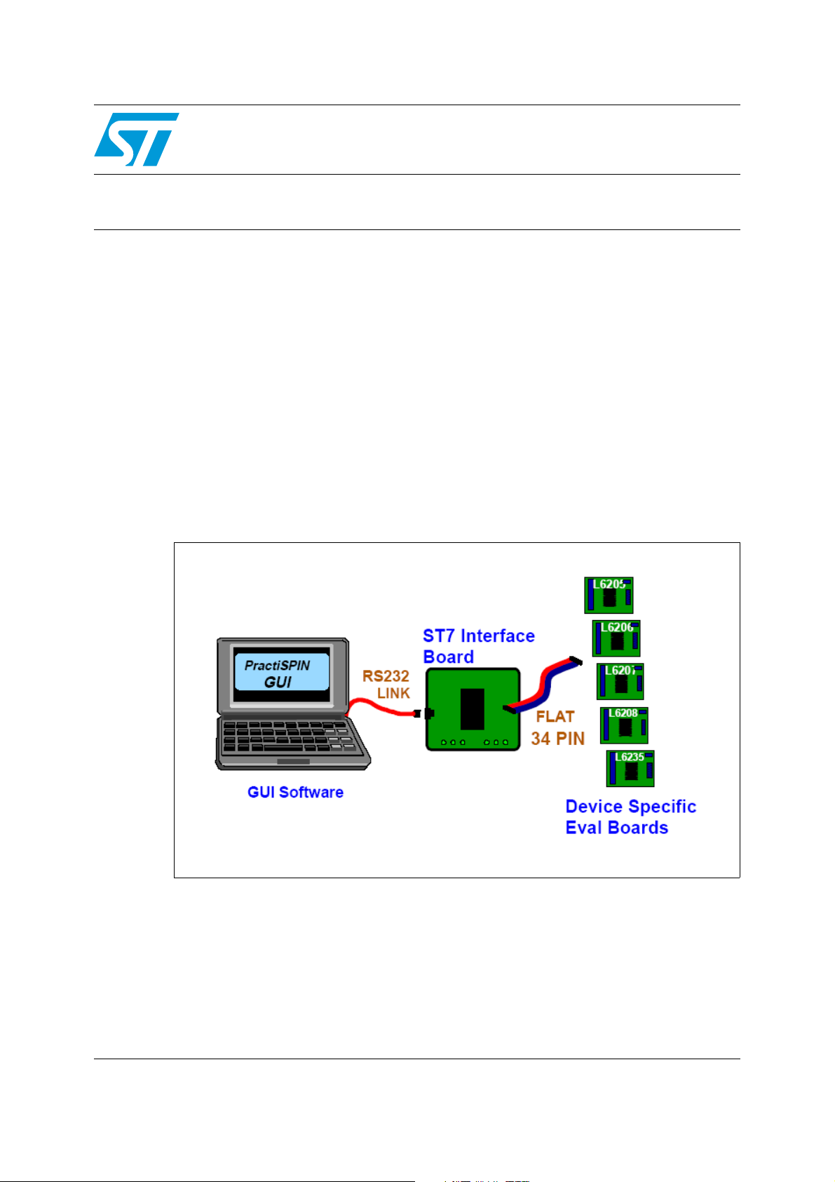
PractiSPIN evaluation system
configuration and set up guide
Introduction
PractiSPIN is an evaluation and demonstration system that can be used with several
STMicroelectronics motor driver integrated circuit devices. The system consists of a
Graphical User Interface (GUI) program which runs on an IBM-PC under windows, a
common ST7 based interface board that communicates with the PC and the practiSPIN
software via a serial COMM port, and a device specific evaluation or target board that
connects to the ST7 interface board via a standard 34 pin ribbon cable interface, as shown
in Figure 1. The target PCB connects to the motor or motors and to a user supplied DC
power supply generally in the range of 12 to 48 Vdc.
The practiSPIN system is designed to operate the device being evaluated (the target device)
under control of the practiSPIN software. Depending on which target device is being used,
the practiSPIN software can operate the device to drive a stepper motor, 1 or 2 DC motors
or a brushless DC (BLDC) motor.
Figure 1. System block diagram
January 2008 Rev 2 1/34
www.st.com
Page 2

Contents AN1794
Contents
1 System overview . . . . . . . . . . . . . . . . . . . . . . . . . . . . . . . . . . . . . . . . . . . . 5
1.1 Target board . . . . . . . . . . . . . . . . . . . . . . . . . . . . . . . . . . . . . . . . . . . . . . . . 5
1.2 Control interface board . . . . . . . . . . . . . . . . . . . . . . . . . . . . . . . . . . . . . . . . 5
2 Starting practiSPIN . . . . . . . . . . . . . . . . . . . . . . . . . . . . . . . . . . . . . . . . . . 7
3 Stepper motor drive . . . . . . . . . . . . . . . . . . . . . . . . . . . . . . . . . . . . . . . . . 8
3.1 Constant speed mode . . . . . . . . . . . . . . . . . . . . . . . . . . . . . . . . . . . . . . . . 8
3.2 Indexing mode . . . . . . . . . . . . . . . . . . . . . . . . . . . . . . . . . . . . . . . . . . . . . . 9
4 DC motor drive . . . . . . . . . . . . . . . . . . . . . . . . . . . . . . . . . . . . . . . . . . . . 10
4.1 Dual DC motor control mode . . . . . . . . . . . . . . . . . . . . . . . . . . . . . . . . . . 10
5 BLDC motor drive . . . . . . . . . . . . . . . . . . . . . . . . . . . . . . . . . . . . . . . . . . 11
5.1 BLDC motor control mode . . . . . . . . . . . . . . . . . . . . . . . . . . . . . . . . . . . . 11
6 EVAL6205N board configuration . . . . . . . . . . . . . . . . . . . . . . . . . . . . . . 12
6.1 Vref offset adjustment (R18) . . . . . . . . . . . . . . . . . . . . . . . . . . . . . . . . . . 14
6.2 Current scaling . . . . . . . . . . . . . . . . . . . . . . . . . . . . . . . . . . . . . . . . . . . . . 14
7 EVAL6206N board configuration . . . . . . . . . . . . . . . . . . . . . . . . . . . . . . 15
7.1 Vref offset adjustment (R18) . . . . . . . . . . . . . . . . . . . . . . . . . . . . . . . . . . 17
7.2 Current scaling . . . . . . . . . . . . . . . . . . . . . . . . . . . . . . . . . . . . . . . . . . . . . 17
8 EVAL6206PD board configuration . . . . . . . . . . . . . . . . . . . . . . . . . . . . . 18
8.1 Vref offset adjustment (R18) . . . . . . . . . . . . . . . . . . . . . . . . . . . . . . . . . . 20
8.2 Current scaling . . . . . . . . . . . . . . . . . . . . . . . . . . . . . . . . . . . . . . . . . . . . . 20
9 EVAL6207N board configuration . . . . . . . . . . . . . . . . . . . . . . . . . . . . . . 21
9.1 Vref offset adjustment (R18) . . . . . . . . . . . . . . . . . . . . . . . . . . . . . . . . . . 23
9.2 Current scaling . . . . . . . . . . . . . . . . . . . . . . . . . . . . . . . . . . . . . . . . . . . . . 23
10 EVAL6208N board configuration . . . . . . . . . . . . . . . . . . . . . . . . . . . . . . 24
10.1 Vref offset adjustment (R18) . . . . . . . . . . . . . . . . . . . . . . . . . . . . . . . . . . 26
2/34
Page 3

AN1794 Contents
10.2 Current scaling . . . . . . . . . . . . . . . . . . . . . . . . . . . . . . . . . . . . . . . . . . . . . 26
11 EVAL6208PD board configuration . . . . . . . . . . . . . . . . . . . . . . . . . . . . . 27
11.1 Vref offset adjustment (R18) . . . . . . . . . . . . . . . . . . . . . . . . . . . . . . . . . . 29
11.2 Current scaling . . . . . . . . . . . . . . . . . . . . . . . . . . . . . . . . . . . . . . . . . . . . . 29
12 EVAL6235 board configuration . . . . . . . . . . . . . . . . . . . . . . . . . . . . . . . 30
12.1 Vref offset adjustment (R18) . . . . . . . . . . . . . . . . . . . . . . . . . . . . . . . . . . 32
12.2 Current scaling . . . . . . . . . . . . . . . . . . . . . . . . . . . . . . . . . . . . . . . . . . . . . 32
13 Revision history . . . . . . . . . . . . . . . . . . . . . . . . . . . . . . . . . . . . . . . . . . . 33
3/34
Page 4

List of figures AN1794
List of figures
Figure 1. System block diagram . . . . . . . . . . . . . . . . . . . . . . . . . . . . . . . . . . . . . . . . . . . . . . . . . . . . . 1
Figure 2. ST7 interface board . . . . . . . . . . . . . . . . . . . . . . . . . . . . . . . . . . . . . . . . . . . . . . . . . . . . . . . 6
Figure 3. EVAL6205N schematic. . . . . . . . . . . . . . . . . . . . . . . . . . . . . . . . . . . . . . . . . . . . . . . . . . . . 13
Figure 4. EVAL6206 schematic . . . . . . . . . . . . . . . . . . . . . . . . . . . . . . . . . . . . . . . . . . . . . . . . . . . . . 16
Figure 5. EVAL6206PD schematic . . . . . . . . . . . . . . . . . . . . . . . . . . . . . . . . . . . . . . . . . . . . . . . . . . 19
Figure 6. EVAL6207N schematic. . . . . . . . . . . . . . . . . . . . . . . . . . . . . . . . . . . . . . . . . . . . . . . . . . . . 22
Figure 7. EVAL6208N schematic. . . . . . . . . . . . . . . . . . . . . . . . . . . . . . . . . . . . . . . . . . . . . . . . . . . . 25
Figure 8. EVAL6208PD schematic . . . . . . . . . . . . . . . . . . . . . . . . . . . . . . . . . . . . . . . . . . . . . . . . . . 28
Figure 9. EVAL6235 schematic . . . . . . . . . . . . . . . . . . . . . . . . . . . . . . . . . . . . . . . . . . . . . . . . . . . . . 31
4/34
Page 5

AN1794 System overview
1 System overview
To illustrate the operation of the practiSPIN system, we will look at one typical device
supported by the system.
The L6207 includes two independent full or H bridges with separate logic inputs and current
control functions.
The two bridges are designated A and B and their output pins designated as OUT1A,
OUT2A, OUT1B, and OUT2B. These outputs are controlled independently by logic inputs
IN1A, IN2A, IN1B, and IN2B respectively.
A logic high or low on any of these inputs will drive its corresponding output to the positive
supply rail or to ground. Both of the A outputs will be forced to an off (high impedance) state
if the ENA pin is taken logic low, as will the B outputs if ENB is taken low. The L6207 is thus
controlled by six logic inputs: IN1A, IN2A, and ENA controlling bridge A and IN1B, IN2B, and
ENB controlling bridge B. Each bridge also has an analog control signal, VREFA and
VREFB, which control the current.
1.1 Target board
The L6207 target board gives access to the bridge A and B outputs at connectors CN3 and
CN4 respectively.
When driving a stepper motor, the two wires from one of the motor windings will connect to
CN3 and the other winding will connect to CN4. Swapping between the two connectors or
swapping the polarity at a given connector will only reverse the sense of motor direction. DC
supply power in the range of 12 to 48 Vdc is connected at CN1. The polarity marked on the
board silkscreen must be strictly observed! The eight control signals are taken from the 34pin ribbon header (CN5) and are driven by the control interface PCB via a short flat cable.
1.2 Control interface board
The control interface PCB is based on an ST72F264 microcontroller. The micro includes a
UART and communicates with the practiSPIN software via 9 pin D connector P1 employing
a standard RS232 interface.
The micro is based on flash memory and its firmware includes a write protected boot-loader
routine that allows the practiSPIN software to update or change the operating program in the
ST7 as required for different target boards. 5 Vdc power for the board is received via the 34pin ribbon cable from the target board or can be directly supplied at J2 if jumper WJ1 is
removed. The eight control signals for the target board are generated by the ST7 micro. The
six logic signals are generated directly by six of the eight pins of port B while the two analog
current references (VREFA and VREFB) are generated by pulse width modulated (PWM)
signals generated by the ST7 along with an offset adjusting circuit controlled by
potentiometer R18.
5/34
Page 6
System overview AN1794
Figure 2. ST7 interface board
6/34
Page 7

AN1794 Starting practiSPIN
2 Starting practiSPIN
Since the practiSPIN system is capable of supporting several driver IC's and driving different
types of motors the user must first select the type of motor to be driven and the driver IC that
will be evaluated.
1. Target board set up: configure the jumpers/switches on the target board and the ST7
interface board as described in the paragraph for the specific evaluation board being
used.
2. Control board - PC connection: connect the ST7 interface board to a serial COMM port
of the PC via a standard (straight through) 9 pin D connector cable.
3. Power up: energize the power supply.
4. Start practiSPIN software: on the PC, start the practiSPIN program.
5. Motor type selection: on the first screen of the practiSPIN software, the user can select
the appropriate type of motor for the device under evaluation. Click on the appropriate
motor type.
6. Communication settings: click the drop down list under "port selection" and select the
COMM port being used. Baud rate and other communication parameters are fixed on
both sides of the link and do not need to be set.
7. Establish COMM link: click the "Connect With ST7 Hardware". At this point the
practiSPIN software will transmit several commands to the ST7 to initialize the
processor. The practiSPIN software will read the revision code of the firmware currently
stored in the flash memory of the ST7 and determine if the correct version of firmware
resides in the ST7. If the practiSPIN software detects that a firmware update is
necessary, either because there is an old version of firmware or the firmware currently
in the flash memory is not the correct firmware for the motor type selected, one or more
dialogue boxes will appear asking if the program should proceed with the update.
Accept the updates and the practiSPIN software will automatically update the firmware.
The system will then initialize the settings to the last stored settings and open the
appropriate practiSPIN software for the selected motor type.
8. Calibrate current setting: when communication is established the user has the option to
adjust the offset and maximum current settings. If this is the first time you use the
system, calibration may be needed to adjust out the offset in the reference bias
circuitry. Calibration ensures that the reference voltage provided to L62XX IC follows
the practiSPIN software current settings. Calibration is a two-step process; first the
offset is adjusted then the maximum current is set.
a) To null out the offset, click on CALIBRATE ZERO then adjust R18 (on ST7 board)
until voltage at Vref pin(s) of the L62XX device is zero. Measurement points on
each board are listed in the set up section for each target board.
b) The maximum current, corresponding to 100% current setting in the practiSPIN
software, can be adjusted using the Vref potentiometers on the target board. If the
potentiometers are set to full scale (clockwise) the reference applied to the input of
the device is typically about 0.88 V. The full-scale peak current is equal to
Vref/Rsense where Rsense is the composite value of the sense resistor on the
board. To set the maximum current, click on CALIBRATE MAX and trim the Vref
potentiometer(s) on the EVAL62XX board to set the desired reference. If you plan
to use microstepping, consider reducing the maximum Vref to the real peak value
you will use, allowing setting the software current controls near to 100%, avoiding
poor Vref resolution.
7/34
Page 8

Stepper motor drive AN1794
3 Stepper motor drive
After the system has established the connection to the interface board, it will initialize the
settings to the last stored settings and open the appropriate GUI for the selected motor type.
For the Stepper motor, the system can operate in either a constant speed or positioning
(indexing) mode. The constant speed mode can easily be used to see that the system is
working.
3.1 Constant speed mode
1. Speed control screen: a large blue button at the bottom of the screen should read,
"switch to INDEXING MODE". If the button reads, "switch to SPEED CONTROL
MODE", click the button once to go to speed control mode.
2. Stepping mode: in the stepping mode box, select either Normal or Half Step.
Microstepping mode is only available when using the L6208.
3. Device selection: in the device selection box, select the device being evaluated.
4. direction: in the direction box, click the toggle switch to pick forward or reverse. This is
somewhat arbitrary since we probably don't know what the direction sense of the motor
will be. Once the motor is running, toggle this switch to reverse the motor direction if
desired. To reverse the meaning of the forward and reverse designations, disable the
motor (orange disable button at bottom of screen) and then swap the motor wires at
either CN3 or CN4.
5. Decay mode: only the L6208 allows the selection of fast or slow decay. Set the toggle
switch to slow decay.
6. Accel rate: set the accel rate to about 1000 steps per second per second (steps/sec2).
In the practiSPIN system all motion parameters are given in terms of the basic units of
steps and seconds: position in steps, velocity in steps/sec, and accel/decel in
steps/sec2. In order to relate these settings to rotations, RPM, and RPM/second it is
necessary to know the number of steps (or half steps) per rotation for the stepper motor
being used. A common value is 200 steps or 400 half steps per rotation.
7. Running speed: set running speed to about 100 steps/sec.
8. Decel rate: set decel. rate to about 1000 steps/sec2.
9. Accel current: set accel current to about 25%. This is an initial guess as to the required
setting and may need further adjustment. Generally higher accel rate settings require
higher accel current settings so that the stepper motor does not start to "slip poles" and
fall behind the desired position. Since we have initially set the acceleration rate setting
quite low, 25% is probably adequate.
10. Running current: set the running current to 25%. In practice the running current can
often be set to a lower value than the accel current since the torque requirement is
generally less during the constant speed part of the move. A lower running current
setting can help to keep the device and the motor running cooler.
11. Decel current: set the decel current to 25%. Since friction aids in decelerating the motor
it may also be possible to set the decel current lower.
12. Holding current: set the holding current to 25%. Whenever the motor is stopped (after a
run,) this level of current will circulate in the motor so that it will hold position against
any mechanical disturbance.
8/34
Page 9

AN1794 Stepper motor drive
In the case of a strong static load (perhaps a gravity load of some sort) it may be necessary
to increase this setting. If not much holding torque is required, then the setting can be
reduced so that operating temperatures can be held to a minimum.
Note: Holding current will be turned off (bridge completely disabled) whenever the disable button
is clicked.
13. Run: make sure that the motor is free to turn in either direction and click the run button.
The motor should quickly come up to speed ((100 steps/sec) / (1000 steps/sec2) = 0.1
sec.). To change the motor direction, click the direction toggle switch. If the motor does
not run click the stop button, increase all four current settings to 50%, and click run
button. If the motor still does not run an oscilloscope and current probe should be used
to observe the motor current.
14. Stop: click stop to stop the motor.
After the basic operation of the system has been verified, the acceleration rates, top speed,
and current settings can be adjusted to see how the motor responds.
3.2 Indexing mode
The system can be switched to operate in the positioning (indexing) mode by clicking on
"switch to INDEXING MODE". In the indexing mode a new box appears on the right of the
screen. You can enter up to twelve indexed movements in the box and the wait time between
each movement. When started, the software will execute each movement by accelerating up
to the peak speed, moving the required number of steps and then decelerating back to a
stop so that the total distance moved is the number of steps indicated, then wait the
indicated time before starting the next movement. A negative number entered in the relative
position will cause the motor to run in the "reverse" direction.
9/34
Page 10

DC motor drive AN1794
4 DC motor drive
After the system has established the connection to the interface board, it will initialize the
settings to the last stored settings and open the appropriate practiSPIN software for the
selected motor type. For DC motor drive, the system operates in an open loop duty cycle
control mode with cycle-by-cycle current limit.
4.1 Dual DC motor control mode
1. Direction: in the direction box for each motor, click the toggle switch to pick forward or
reverse. This is somewhat arbitrary since we probably don't know what the direction
sense of the motor will be. Once the motor is running, toggle this switch to reverse the
motor direction if desired. To reverse the meaning of the forward and reverse
designations, disable the motor (orange disable button at bottom of screen) and then
swap the motor wires at either CN3 or CN4.
2. Braking: toggle the "Brake when Stop" switch to the OFF position for both motors. This
will cause the motor to coast to rest when stopped, with the bridge placed in a high
impedance state. If desired this function can later be toggled on but some care should
be exercised. Braking will effectively short out the motor armature through two
transistors in the bridge, which could cause excessive current and power dissipation if
the motor and load have a large moment of inertia (thus a large amount or stored
mechanical to be dissipated) or the motor has a very low resistance (resulting in a large
current flow). Most smaller DC motors with several ohms of resistance do not pose a
risk.
3. Current: set the current for both motors to approximately 25%. This is an initial guess
as to the required setting and may need further adjustment.
4. Voltage: set the voltage for both motors to approximately 50%.
5. Run: make sure that the motors are free to turn in either direction and click the run
button. the motors should come up to approximately half of the speed that would be
expected at this supply voltage. To change the motor direction, click the direction toggle
switch. If the motors do not run click the STOP button, increase both current settings to
50%, and click RUN button. If the motors still do not run an oscilloscope and current
probe should be used to observe the motor current
6. Stop: click stop to stop the motor.
After the basic operation of the system has been verified, adjust voltage, current, direction
and other parameters to evaluate the system.
10/34
Page 11

AN1794 BLDC motor drive
5 BLDC motor drive
After the system has established the connection to the interface board, it will initialize the
settings to the last stored settings and open the appropriate practiSPIN software for the
selected motor type. For BLDC motor drive, the system operates in an open loop duty cycle
control mode with cycle-by-cycle current limit.
5.1 BLDC motor control mode
1. Direction: in the direction box for each motor, click the toggle switch to pick forward or
reverse. This is somewhat arbitrary since we probably don't know what the direction
sense of the motor will be. Once the motor is running, toggle this switch to reverse the
motor direction if desired.
2. Braking: toggle the "Brake when Stop" switch to the OFF position. This will cause the
motor to coast to rest when stopped, with the bridge placed in a high impedance state.
If desired this function can later be toggled on but some care should be exercised.
Braking will effectively short out the motor armature through three transistors in the
bridge, which could cause excessive current and power dissipation if the motor and
load have a large moment of inertia (thus a large amount or stored mechanical to be
dissipated) or the motor has a very low resistance (resulting in a large current flow).
Most smaller BLDC motors with several ohms of resistance do not pose a risk.
3. Current: set the current to approximately 25%. This is an initial guess as to the required
setting and may need further adjustment.
4. Voltage: set the voltage to approximately 50%.
5. Run: make sure that the motor is free to turn in either direction and click the run button.
The motor should come up to approximately half of the speed that would be expected
at this supply voltage. To change the motor direction, click the direction toggle switch. If
the motor does not run click the stop button, increase the current settings to 50%, and
click run button. If the motor still does not run an oscilloscope and current probe should
be used to observe the motor current.
6. Stop: click stop to stop the motor.
After the basic operation of the system has been verified, adjust voltage, current, direction
and other parameters to evaluate the system.
11/34
Page 12

EVAL6205N board configuration AN1794
6 EVAL6205N board configuration
The schematic of the EVAL6205N board is shown in Figure 3. To use the EVAL6205N board
with practiSPIN system, the following configuration settings must be made on the
EVAL6205N:
1. Component updates: depending on the revision of the board, some or all of the
following changes may be required (or desirable):
a) To assure safe overcurrent operation: change C6 and C7 to 5.6 nF Change R5
and R6 to 100 kΩ.
b) To assure an adequate 5 V supply, R2 may need to be changed. The minimum
value for R2 is (Vs-5)/(0.03+I) Ω . Where: Vs is the supply voltage and I is any
additional load placed on the 5 V supply (in amps).
2. JP1: place JP1 in the INT position to enable the on-board 5 Vdc supply.
3. JP2 and JP3: install JP2 and JP3 to assure proper timing operation of the L6205's
internal high side overcurrent protection.
4. JP4 and JP5: install JP4 and JP5 to configure the Vref circuits.
5. R17 & R21: adjust multi-turn trim potentiometers R17 and R21 fully clockwise.
Note: A slight click can be heard from the pot when it reaches its end of travel.
6. R23 Adjust multi-turn trim pot R23 to the middle of its range. This pot sets the
frequency of the cycle-bycycle current controller and can be fine tuned while observing
the motor current on an oscilloscope or by simply adjusting to raise the frequency of the
audible switching noise to an inaudible level if required.
7. Motor connections: connect the motor coils at CN3 and CN4. When driving a stepper
motor, one winding is connected to CN3 and the second winding is connected to CN4.
For operation with 2 DC motors one motor is connected to each connector.
8. Power supply: connect, but do not energize, a 12 to 48 Vdc power supply at CN1
(positive to V
9. Using a 34 pin ribbon cable connect the EVAL6205N board to the control interface
board. The two boards should be placed on the bench so that their 34 pin headers are
side by side with the ribbon cable going straight across. Set the following on the ST7
interface board.
10. WJ1: install WJ1 on the ST7 based control interface board. This allows 5 Vdc power to
be obtained from the target board.
11. JP1 and JP2 and R18: install the JP1 and JP2 jumpers to short the center and left pins
together as shown in Figure 2. This is critical as excessive motor current can result
from misplacement of these jumpers! Set potentiometer R18 to about 50%.
and negative to GND).
in
12/34
Page 13

AN1794 EVAL6205N board configuration
Figure 3. EVAL6205N schematic
IN2
IN4
LIMIT_A
ENA
1
2
1
CN1
D2
D1
2
CN2
GND
D3
R2
C5
VCCREF
int .
2
JP1
1 3
ext.
+5V
C3
U1
14
17
C4
R1
19
12
C2
C1
15
16
6
5
1
2
CN3
CN4
PullUp
7
18
4
OUT1 B
OUT2 A
OUT1 A
VSB
VSA
VCP
VBOOT
GND
GND
GND
GND
IN1
1
L6205
ENB
ENA
IN2
2
11
20
LIMIT_B
1
2
INT6
INT0
INT2
INT3
246
8
13579111315171921232527293133
ADC_REF
PullUp
13
OUT2 B
SENSEB
SENSEA
IN3
IN4
9
10
TINA0 P2.0
TOUTB0 P2.3
10121416182022242628303234
+5V
8
3
JP3
ENB
IN1
IN3
TOUTA1 P2.6
TINB0 P2.1
TO UTP B1 2.7
TI NA1 P2 .4
TINB1 P2.5
PullUp
CN5
VREF_A
OCMPB1/ICAPB1 P4.3
OCMPA1 P4.2
R16
VREFB
VREFA
JP4
CW
R15
PullUp
R17
R13
PullUp
R12
R11
R10
R9
R8
R7
C6
C7
SENSE_B
SENSE_A
_4
_3
_2
_1
R19
VREF_B
R20
C9
C12
9
U2
Vref2
17
Vref1Sync
GND
163
Vsense2
15
Vsense1
10
EN
4
Out4
11
Out3
12
Out2
13
Out1
14
CW
R21
JP5
C13
Osc_Out
2
R/C
1
In 4
8
In 3
7
L6506D ip
In2
6
In1
5
VCC
18
C11
R23
IN4
IN3
IN2
R22
IN1
PullUp
CW
R6
R4
PullUp
R3
R5
_2
_1
_3
ENB
ENA
JP2
R14
_4
1
2
3
4
LI MIT_ A
LI MIT_ B
R18
C8
SENSE_ A
C10
SENSE_ B
13/34
Page 14

EVAL6205N board configuration AN1794
6.1 Vref offset adjustment (R18)
Using a voltmeter monitor the voltage at jumper JP4 or JP5 the EVAL6205N board with
respect to GND (CN1) when calibrating the offset.
6.2 Current scaling
When potentiometers R17 and R21 are set full clockwise, a 100% current setting on the
practiSPIN software screen corresponds to a Vref of approximately 0.88 Vdc or a peak
motor current of about 2.64 A.
The peak current can be set to a lower value by adjusting R17 and R21. The reference
voltage inputs can be monitored at JP4 and JP5.
14/34
Page 15

AN1794 EVAL6206N board configuration
7 EVAL6206N board configuration
The schematic of the EVAL6206N board is shown in Figure 4. To use the EVAL6206N board
with practiSPIN system, the following configuration settings must be made on the
EVAL6206N:
1. Component updates: depending on the revision of the board, some or all of the
following changes may be required (or desirable):
a) To assure safe overcurrent operation:
– Change C6 and C7 to 5.6 nF
– Change R5 and R6 to 100 kΩ
b) To assure an adequate 5 V supply, R2 may need to be changed. The minimum
value for R2 is (Vs-5)/(0.03+I) Ω . Where: Vs is the supply voltage and I is any
additional load placed on the 5 V supply (in amps).
2. JP1: place JP1 in the INT position to enable the on-board 5 Vdc supply.
3. JP2 and JP3: install JP2 and JP3 to enable the L6206's internal high side overcurrent
protection.
4. JP4 and JP5: install JP4 and JP5 to set internal overcurrent threshold to maximum. If
desired, these jumpers can be left out and the overcurrent levels may be set using
potentiometers R7 and R8.
5. JP6 and JP7: install JP6 and JP7 to configure the Vref circuits.
6. R20 and R26 adjust multi-turn trim pots R20 and R26 fully clockwise.
Note: A slight click can be heard from the pot when it reaches its end of travel.
7. R29: adjust multi-turn trim pot R29 to the middle of its range. This pot sets the chopping
frequency of the L6506 current controller and can be fine tuned while observing the
motor current on an oscilloscope or by simply adjusting to raise the frequency of the
audible switching noise to an inaudible level if required.
8. Motor connections: connect the motor coils at CN3 and CN4. When driving a stepper
motor, one winding is connected to CN3 and the second winding is connected to CN4.
For operation with 2 DC motors one motor is connected to each connector.
9. Power supply: connect, but do not energize, a 12 to 48 Vdc power supply at CN1
(positive to V
10. Using a 34 pin ribbon cable connect the EVAL6205N board to the control interface
board. The two boards should be placed on the bench so that their 34 pin headers are
side by side with the ribbon cable going straight across. Set the following on the ST7
interface board.
11. WJ1: install WJ1 on the ST7 based Control Interface Board. This allows 5 Vdc power to
be obtained from the target board.
12. JP1 and JP2 and R18: install the JP1 and JP2 jumpers to short the center and left pins
together as shown in Figure 2. This is critical as excessive motor current can result
from misplacement of these jumpers! Set potentiometer R18 to about 50% .
and negative to GND).
in
15/34
Page 16

EVAL6206N board configuration AN1794
Figure 4. EVAL6206 schematic
OCDA
ENA
1
2
1
2
CN2
CN1
1
2
CN4
CN3
OCDB
1
2
IN2
ENB
IN4
IN1
IN3
TOUTB0 P2.3
INT6
INT0
INT2
INT3
246
GND
D3
R2
C5
VCCREF
int.
2
JP1
PullUp
1 3
ext.
+5V
C3
5
8
16
U1
L6206
17
20
D2
R1
22
D1
C4
15
C2
19
C1
18
7
6
R4
PullU p
R3
21
OUT1A
OUT1B
OUT2A
VSB
VSA
VCP
VBOOT
GND
GND
GND
GND
IN1
IN2
ENB
ENA
1
2
R5
_2
_1
11
14
23
R6
ENB
ENA
8
10121416182022242628303234
13579111315171921232527293133
ADC_REF
PullUp
PullUp
OUT2B
SENSEB
10
SENSEA
3
PROGCLB
13
PROGCL A
24
OCDB
9
OCDA
4
IN3
IN4
12
1
2
3
4
_3
_4
TINB1 P2.5
TOUTA1 P2.6
TINB0 P2.1
TOUTPB1 2.7
TINA0 P2.0
+5V
R17
CW
CW
JP3
JP2
TINA1 P2.4
CN5
OCMPB1/ICAPB1 P4.3
OCMPA1 P4.2
VREFA
VREFB
PROGCLB
PROGCLA
CW
JP6
R20
R16
PullUp
R14
R13
R12
R11
R10
R9
R8
R7
C7
C6
R15
OCDA
OCDB
VREF_ A
VREF_ B
PullUp
R23
R25
R19
C9
C13
9
U2
L6506Dip
Vref2
Vref1Sync
EN
Out4
Out3
Out2
Out1
C10
Osc_Out
GND
Vsense2
R/C
Vsense1
In4
In3
In2
In1
VCC
18
R24
17
163
SENSE_B
15
10
SENSE_A
4
_4
11
_3
12
_2
13
_1
14
JP5
JP4
C8
R18
PROGCLA
R22
R21
PROGCLB
CW
R26
JP7
C15
2
1
8
7
6
5
C11
C12
SENSE_A
R29
IN4
IN3
IN2
IN1
PullUp
R27
SENSE_B
CW
R28
C14
16/34
Page 17

AN1794 EVAL6206N board configuration
7.1 Vref offset adjustment (R18)
Using a voltmeter monitor the voltage at jumper JP6 or JP7 the EVAL6206N board with
respect to GND (CN1) when calibrating the offset.
7.2 Current scaling
When potentiometers R20 and R26 are set full clockwise, a 100% current setting on the
practiSPIN software screen corresponds to a Vref of approximately 0.88 Vdc or a peak
motor current of about 2.64 A.
The peak current can be set to a lower value by adjusting R17 and R21. The reference
voltage inputs can be monitored at JP6 and JP7.
17/34
Page 18

EVAL6206PD board configuration AN1794
8 EVAL6206PD board configuration
The schematic of the EVAL6206PD board is shown in Figure 5. To use the EVAL6206PD
board with practiSPIN system, the following configuration settings must be made on the
EVAL6206PD:
1. Component updates: depending on the revision of the board, some or all of the
following changes may be required (or desirable):
a) To assure safe overcurrent operation:
– Change C6 and C7 to 5.6 nF
– Change R4 and R5 to 100 kΩ
b) To assure an adequate 5 V supply, R1 may need to be changed. The minimum
value for R1 is (Vs-5)/(0.03+I) Ω . Where: Vs is the supply voltage and I is any
additional load placed on the 5 V supply (in amps).
2. JP1: place JP1 in the INT position to enable the on-board 5 Vdc supply.
3. JP2 and JP3: install JP2 and JP3 to enable the L6206's internal high side overcurrent
protection.
4. JP4 and JP5: install JP4 and JP5 to set internal overcurrent threshold to maximum. If
desired, these jumpers can be left out and the overcurrent levels may be set using
potentiometers R6 and R7.
5. R16 and R22: adjust multi-turn trim pots R16 and R22 fully clockwise.
Note: A slight click can be heard from the pot when it reaches its end of travel.
6. R25 Adjust multi-turn trim pot R25 to the middle of its range. This pot sets the chopping
frequency of the L6506 current controller and can be fine tuned while observing the
motor current on an oscilloscope or by simply adjusting to raise the frequency of the
audible switching noise to an inaudible level if required.
7. Motor connections: connect the motor coils at CN3 and CN4. When driving a stepper
motor, one winding is connected to CN3 and the second winding is connected to CN4.
For operation with 2 DC motors one motor is connected to each connector.
8. Power supply: connect, but do not energize, a 12 to 48 Vdc power supply at CN1
(positive to V
and negative to GND).
in
9. Using a 34 pin ribbon cable connect the EVAL6205N board to the control interface
board. The two boards should be placed on the bench so that their 34 pin headers are
side by side with the ribbon cable going straight across.
Set the following on the ST7 interface board
● WJ1: Install WJ1 on the ST7 based control interface board. This allows 5 Vdc power to
be obtained from the target board.
● JP1 and JP2 and R18: install the JP1 and JP2 jumpers to short the center and left pins
together as shown in Figure 2. This is critical as excessive motor current can result
from misplacement of these jumpers! Set potentiometer R18 to about 50%.
18/34
Page 19

AN1794 EVAL6206PD board configuration
Figure 5. EVAL6206PD schematic
IN2
ENA
OCDB
1
1
2
1
CN1
2
CN2
D2
R1
CN3
2
1
2
CN4
OCDA
INT2
INT6
INT3
INT0
246
8
10121416182022242628303234
13579111315171921232527293133
A0IN6 P7.6
ADC_REF
A1IN6 P8.1
IN3
ENB
IN1
IN4
VREF_A
TINA0 P2.0
TOUTB0 P2.3
TINA1 P 2.4
TINB1 P2.5
TOUTA1 P2.6
TINB0 P2.1
TOUTPB1 2.7
CN5
OCMPA1 P4.2
OCMPB1/ICAPB1 P4.3
R14
VREF_B
R20
PullU p
R19
CW
R22
STMicroelectronics Industrial&Power Supply Application LAB
C5
VCCREF
int.
2
PullUp
1 3
ext.
JP1
+5V
C3
15
2361416
NCNCNCNCNC
VSB
33
VSA
13
D1
C1
4
C4
2
C2
VCPPROGCL B
728
VBOOT
30
GND
19
GND
18
GND
1
GND
36
IN1
10
22532
17
20
2123313435
NC
NC
OUT1B
OUT2B
NCNCNCNCNC
OUT1A
OUT2A
U1
L6206PD
IN2
11
IN3
ENB
ENA
8
26
29
+5V
PullUp
SENSE_A
SENSE_B
VREFA
VREFB
PROGCLB
PROGCLA
CW
PullUp
R12
R16
R26
PullUp
SENSEB
25
SENSEA
12
R11
R10
R9
R8
R7
CW
PROGCL A
R6
9
CW
OCDB
24
C6
OCDA
13
IN4
27
JP3
C7
R13
C9
C13
C14
910
Vref2
Vref1Sync
EN
Out4
Out3
Out2
Out1
NC
11
R18
Osc_Out
2
GNDNC
Vsense2
R/C
1
Vsense1
In4
8
In3
7
In2
6
In1
5
VCC
20
C11
C10
IN4
IN3
IN2
IN1
PullUp
CW
R25
R24
19
183
SENSE_B
17
12
SENSE_A
4
_4
13
_3
14
_2
15
_1
16
U2
JP5
JP4
C8
R15
R17
R4
R3
PullUp
R2
_1
R5
_2
_3
ENB
ENA
JP2
R21
_4
OCDA
OCDB
PROGCLA
PROGCLB
SENSE_A
R23
C12
C15
SENSE_B
19/34
Page 20

EVAL6206PD board configuration AN1794
8.1 Vref offset adjustment (R18)
Using a voltmeter monitor the voltage at the junction of R12 and R16 or the Junction of R20
and R22 on the EVAL626PD board with respect to GND (CN1) when calibrating the offset.
8.2 Current scaling
When potentiometers R16 and R22 are set full clockwise, a 100% current setting on the
practiSPIN software screen corresponds to a Vref of approximately 0.88 Vdc or a peak
motor current of about 4.4 A. The peak current can be set to a lower value by adjusting R16
and R22.
20/34
Page 21

AN1794 EVAL6207N board configuration
9 EVAL6207N board configuration
The schematic of the EVAL6207N board is shown in Figure 6. To use the EVAL6207N board
with practiSPIN system, the following configuration settings must be made on the
EVAL6207N:
1. Component updates: depending on the revision of the board, some or all of the
following changes may be required (or desirable):
a) To assure safe overcurrent operation:
– Change C6 and C7 to 5.6 nF
– Change R3 and R4 to 100 kΩ
b) To assure an adequate 5 V supply, R2 may need to be changed. The minimum
value for R2 is (Vs-5)/(0.03+I) Ω . Where: Vs is the supply voltage and I is any
additional load placed on the 5 V supply (in amps).
2. JP1: place JP1 in the INT position to enable the on-board 5 Vdc supply.
3. JP2 and JP3: install JP2 and JP3 to assure proper timing operation of the L6207's
internal high side overcurrent protection.
4. R15 and R18: adjust multi-turn trim pots R15 and R18 fully clockwise.
Note: A slight click can be heard from the pot when it reaches its end of travel.
5. R6 and R7: adjust multi-turn trim pots R6 and R7 to the middle of their range. These
pots set the off time of the cycle by cycle current controller and can be fine tuned while
observing the motor current on an oscilloscope or by simply adjusting to raise the
frequency of the audible switching noise to an inaudible level if required.
6. motor connections: connect the motor coils at CN3 and CN4. When driving a stepper
motor, one winding is connected to CN3 and the second winding is connected to CN4.
For operation with 2 DC motors one motor is connected to each connector.
7. Power supply: connect, but do not energize, a 12 to 48 Vdc power supply at CN1
(positive to V
8. Using a 34 pin ribbon cable connect the EVAL6207N board to the control interface
Board. The two boards should be placed on the bench so that their 34 pin headers are
side by side with the ribbon cable going straight across. Set the following on the ST7
interface board
9. WJ1: install WJ1 on the ST7 based Control Interface Board. This allows 5 Vdc power to
be obtained from the target board.
10. JP1 and JP2 and R18: install the JP1 and JP2 jumpers to short the center and left pins
together as shown in Figure 2. This is critical as excessive motor current can result
from misplacement of these jumpers! Set potentiometer R18 to about 50%.
and negative to GND).
in
21/34
Page 22

EVAL6207N board configuration AN1794
Figure 6. EVAL6207N schematic
1
1
CN3
1
2
CN 1
R2
VCCRE F
int.
1 3
ext.
+5 V
C3
GND
1
2
CN 2
D3
C5
2
JP1
PullUp
2
2
CN4
ENA
LIMIT_B
LIMIT_A
RC A /INH
INT0
INT2
TINPA O P2.0
TOUTA O P2.2
246
8
10121416182022242628303234
13579111315171921232527293133
CN 5
ADC_R EF
A0IN6 P7.6
A1IN6 P8.1
VCCREF
SENSE_A
SENSE_B
+5 V
TINPB 0 P2.1
IN2
IN3
TOUTB 1 P2.7
ENB
IN4
TOUTA 1 P2.6
OCMPA 0/ICAPA0 P3. 2
OCMPA 1 P 4.2
OCMPB 0 P 3.3
OCMPB 1/ICAPB1 P4. 3
VREFB
VREFA
LIMIT_A
LIMIT_B
IN1
VSB
VSA
VCP
GND
GND
GND
GND
5
VBOOT
IN1A
1
2
IN1
U1
17
20
D2
D1
ENB
C4
R1
C2
C1
ENA
22
15
19
18
7
6
8
OUT2A
L6207
ENA
14
LI MIT _A
LIMITB
R4
16
OUT1B
OUT2B
IN1B
ENB
IN2B
11
12
LI MIT _B
IN3
IN4
JP3
JP2
SENSEB
SENSEB
10
SENSEA
SENSEA
3
RCB
9
RCA/I NH
4
VREF B
13
C9
VREF B
VREF A
24
VREF A
C8
PullUp
R5
C7
C6
R14
R1 3
R12
R1 1
R10
R9
CW
R7
C1 1
C10
R6
CW
R1 6
Pu llUp
R1 8
CW
R1 7
R15
R8
VRE F_A
VRE F_B
RCA/I NH
21
OUT1A
IN2A
23
IN2
LIMITA
R3
22/34
Page 23

AN1794 EVAL6207N board configuration
9.1 Vref offset adjustment (R18)
Using a voltmeter monitor the voltage at the VrefA or VrefB test point on the EVAL6207N
board with respect to GND (CN1) when calibrating the offset.
9.2 Current scaling
When potentiometers R20 and R26 are set full clockwise, a 100% current setting on the
practiSPIN software screen corresponds to a Vref of approximately 0.88 Vdc or a peak
motor current of about 2.64 A.
The peak current can be set to a lower value by adjusting R15 and R18. The reference
voltage inputs can be monitored at the VrefA or VrefB test point.
23/34
Page 24

EVAL6208N board configuration AN1794
10 EVAL6208N board configuration
The schematic of the EVAL6208N board is shown in Figure 7. To use the EVAL6208N board
with practiSPIN system, the following configuration settings must be made on the
EVAL620A:
1. Component updates: depending on the revision of the board, some or all of the
following changes may be required (or desirable):
a) To assure safe overcurrent operation:
– Change C6 to 5.6 nF
– Change R9 to 100 kΩ
b) To assure an adequate 5 V supply, R2 may need to be changed. The minimum
value for R2 is (Vs-5)/(0.03+I) Ω . Where: Vs is the supply voltage and I is any
additional load placed on the 5 V supply (in amps).
2. JP1: place JP1 in the INT position to enable the on-board 5 Vdc supply.
3. Switches place all four of the switches in the right (toward the L6208) position.
4. R20 and R24: adjust multi-turn trim pots R20 and R24 fully clockwise.
Note: A slight click can be heard from the pot when it reaches its end of travel.
5. R11 and R12: adjust multi-turn trim pots R11 and R12 to the middle of their range.
These pots set the off time of the cycle by cycle current controller and can be fine tuned
while observing the motor current on an oscilloscope or by simply adjusting to raise the
frequency of the audible switching noise to an inaudible level if required.
6. Motor connections: connect the motor coils at CN3 and CN4. When driving a stepper
motor, one winding is connected to CN3 and the second winding is connected to CN4.
For operation with 2 DC motors one motor is connected to each connector.
7. Power supply: connect, but do not energize, a 12 to 48 Vdc power supply at CN1
(positive to V
8. Using a 34 pin ribbon cable connect the EVAL6208N board to the control interface
Board. The two boards should be placed on the bench so that their 34 pin headers are
side by side with the ribbon cable going straight across. Set the following on the ST7
interface board.
9. WJ1: install WJ1 on the ST7 based control interface board. This allows 5 Vdc power to
be obtained from the target board.
10. JP1 and JP2 and R18: install the JP1 and JP2 jumpers to short the center and left pins
together as shown in Figure 2. This is critical as excessive motor current can result
from misplacement of these jumpers! Set potentiometer R18 to about 50%.
and negative to GND).
in
24/34
Page 25

AN1794 EVAL6208N board configuration
Figure 7. EVAL6208N schematic
1
2
CN1
D2
R2
int.
JP1
ext.
C3
1
2
CN2
GND
D3
VCCREF
2
PullUp
1 3
+5V
17
20
C4
R1
22
1
2
CN3
5
OUT1A
VSB
VSA
VCP
1
2
CN4
81516
21
OUT1B
OUT2A
OUT2B
DI A G
246
13579111315171921232527293133
CN5
PullUp
SENSEB
SENSEA
RCB
EN
RC A
8
10121416182022242628303234
+5V
U1
10
3
RCB
9
RESET
CW/ CCW
CL OC K
CON TROLC5HAL F /F UL L
CLOC K
VREFB
VREFA
R19
R18
R17
R16
R15
R14
CW
R12
D1
VBOOT
C2
RCA
L6208N
GND
19
GND
C1
EN
9
10
11
12
13
14
15
16
PullUp
8
7
CW
6
5
CCW
SLOW
4
3
FAST
HALF
2
1
FULL
S1
18
GND
7
GND
6
CLOC K
1
R8
R7
R6
R5
R4
PullUp
R3
PullUp
CL OC K
CLOC K
CONT ROL
CW/ CCW
2
CW/ CCW
HALF /FULL
13
CONT ROL
HALF /FULL
VREFB
VREF A
EN
RESET
142312
R9
DIA G
EN
RESET
DIA G
RCA
4
RCA
C8
11
VREF B
24
C7
VREF A
C6
R1 0
PullUp
C10
C9
R11
CW
R21
PullUp
CW
R2 4
CW
R20
R13
VREFA
R22
VREFB
25/34
Page 26

EVAL6208N board configuration AN1794
10.1 Vref offset adjustment (R18)
Using a voltmeter monitor the voltage at the VrefA or VrefB test point on the EVAL6208N
board with respect to GND (CN1) when calibrating the offset.
10.2 Current scaling
When potentiometers R20 and R21 are set full clockwise, a 100% current setting on the
practiSPIN software screen corresponds to a Vref of approximately 0.88 Vdc or a peak
motor current of about 2.64 A.
The peak current can be set to a lower value by adjusting R15 and R18. The reference
voltage inputs can be monitored at the VrefA or VrefB test point
After tube recognition the microcontroller will set the right run frequency for the connected
lamp.
26/34
Page 27

AN1794 EVAL6208PD board configuration
11 EVAL6208PD board configuration
The schematic of the EVAL6208PD board is shown in Figure 8. To use the EVAL6208PD
board with practiSPIN system, the following configuration settings must be made on the
EVAL6208PD:
1. Component updates: depending on the revision of the board, some or all of the
following changes may be required (or desirable):
a) To assure safe overcurrent operation:
– Change C12 to 5.6 nF
– Change R21 to 100 kΩ
b) To assure an adequate 5 V supply, R1 may need to be changed. The minimum
value for R1 is (Vs-5)/(0.03+I) Ω . Where: Vs is the supply voltage and I is any
additional load placed on the 5 V supply (in amps).
2. JP1: place JP1 in the INT position to enable the on-board 5 Vdc supply.
3. Switches: place all four of the switches in the right (toward the L6208) position.
4. R8 and R17: adjust multi-turn trim pots R8 and R17 fully clockwise.
Note: A slight click can be heard from the pot when it reaches its end of travel.
5. R10 and R11: adjust multi-turn trim pots R10 and R11 to the middle of their range.
These pots set the off time of the cycle by cycle current controller and can be fine tuned
while observing the motor current on an oscilloscope or by simply adjusting to raise the
frequency of the audible switching noise to an inaudible level if required.
6. Motor connections: connect the motor coils at CN3 and CN4. When driving a stepper
motor, one winding is connected to CN3 and the second winding is connected to CN4.
For operation with 2 DC motors one motor is connected to each connector.
7. Power supply: connect, but do not energize, a 12 to 48 Vdc power supply at CN1
(positive to V
8. Using a 34 pin ribbon cable connect the EVAL6208PD board to the control interface
board. The two boards should be placed on the bench so that their 34 pin headers are
side by side with the ribbon cable going straight across. Set the following on the ST7
interface board.
9. WJ1: install WJ1 on the ST7 based control interface board. This allows 5 Vdc power to
be obtained from the target board.
10. JP1 and JP2 and R18: install the JP1 and JP2 jumpers to short the center and left pins
together as shown in Figure 2. This is critical as excessive motor current can result
from misplacement of these jumpers! Set potentiometer R18 to about 50%.
and negative to GND).
in
27/34
Page 28

EVAL6208PD board configuration AN1794
Figure 8. EVAL6208PD schematic
1
1
2
CN1
1
2
CN2
1
CN3
2
2
CN4
RCA
DIA G
D2
R1
C5
VCCREF
int.
2
PullUp
JP 1
1 3
ext.
VIN
13
R1 8
2
D1
C1
C2
S1
EN
9
10
11
12
13
14
15
16
Pul lUp
8
7
CW
6
5
CCW
SLOW
4
3
FAST
HALF
2
1
FULL
Pul lUp
PullUp
JUMPER 3x1
+5V
C3
NCNCNCNCNC
VSB
VSA
VCP
VBO OT
GND
GND
GND
GND
CLOCK
10
CL OCK
CL OCK
15
CW/ CCW
11
CW/ CCW
2361416
U1
33
4
7
C4
30
19
18
36
1
GND
R7
R6
R5
R4
R3
R2
22532
17
20
2123313435
NC
NC
L6208PD
27
NCNCNCNCNC
OUT1B
OUT2B
SENSEB
25
SENSEA
12
RCB
24
RCA
13
VREFB
26
VREF B
VREF A
9
EN
HAL F/FUL L
29
R21
EN
HAL F/FUL L
VREF A
RESE T
8
C1 2
Pul lUp
DIAG
RES ET
OUT1A
OUT2A
CONTROL
28
CON T RO L
246
13579111315171921232527293133
CN 5
ADC_R EF
PullUp
SENSEB
SENSEA
R1 1
R10
C9
C6
R1 6
R9
VREF_A
EN
TOUTA 0 P2.2
TINA0 P2.0
TOUTB 0 P2.3
8
10121416182022242628303234
+5V
R1 5
R1 4
R1 3
R1 2
CW
C8
C7
CW
PullUp
R8
CW/ CCW
CONTROL
HAL F/FUL L
CL OCK
RES ET
TOUTB1 P2.7
TOUTA 1 P2.6
TINB1 P2.5
TINA1 P2.4
CON34A
STMicroe lectr onics Industria l &Power S upply Ap plicatio n LAB
OCMPA 1 P 4.2
OCMPB1 /ICAPB1 P4.3
VREFB
VREFA
CLOCK
CW
R2 0
R1 7
CW
R1 9
VREF_B
RC A
28/34
Page 29

AN1794 EVAL6208PD board configuration
11.1 Vref offset adjustment (R18)
Using a voltmeter monitor the voltage at the VrefA or VrefB test point on the EVAL6208PD
board with respect to GND (CN1) when calibrating the offset.
11.2 Current scaling
When potentiometers R8 and R17 are set full clockwise, a 100% current setting on the
practiSPIN software screen corresponds to a Vref of approximately 0.88 Vdc or a peak
motor current of about 4.4 A. The peak current can be set to a lower value by adjusting R15
and R18. The reference voltage inputs can be monitored at the VrefA or VrefB test point.
29/34
Page 30

EVAL6235 board configuration AN1794
12 EVAL6235 board configuration
The schematic of the EVAL6235 board is shown in Figure 9. To use the EVAL6235 board
with practiSPIN system, the following configuration settings must be made on the
EVAL6235:
1. Component updates: depending on the revision of the board, some or all of the
following changes may be required (or desirable):
a) To assure safe overcurrent operation:
– Change C6 and C7 to 5.6 nF
– Change R6 to 100 kΩ and remove R2
b) To assure an adequate 5 V supply, R1 may need to be changed. The minimum
value for R1 is (Vs-5)/(0.03+I) Ω . Where: Vs is the supply voltage and I is any
additional load (such as Hall sensors) placed on the5 V supply (in amps).
2. JP1 and JP2: install JP1 and JP2 to enable the on-board 5 Vdc supply.
3. Switches: place all four switches in the down (away from U2) position.
4. R22: adjust multi-turn trim pot R22 fully clockwise.
Note: A slight click can be heard from the pot when it reaches its end of travel.
5. R10: adjust multi-turn pot R10 to the middle of its range. This pot sets the off time of the
cycle by cycle current controller and can be fine tuned while observing the motor
current on an oscilloscope or by simply adjusting to raise the frequency of the audible
switching noise to an inaudible level if required.
6. Hall sensors: connect the hall sensors of the BLDC motor at CN5. Connect the power
supply wires from the hall sensors at pins GND and P5V. Hall sensors are notorious for
being destroyed by reversed polarity! Know, don't guess, the proper polarity! Connect
H1, H2, and H3 signals to their respective pins.
7. Motor connections: connect the three motor armature wires at CN3 being careful to
match the phasing to the hall sensor connections. Please refer to the L6235 data sheet
for a description of the proper phase relationship between the motor phases and the
Hall sensors.
Note: There are six possible ways to connect the three armature wires to CN3. While only one
connection will give proper performance, one or two of the other possible connection may
cause the motor to turn but with very poor performance and, perhaps, high motor currents
even if the system is unloaded.
8. Power supply: connect, but do not energize, a 12 to 48 Vdc power supply at CN1
(positive to V
9. Using a 34 pin ribbon cable connect the EVAL6208PD board to the control interface
board. The two boards should be placed on the bench so that their 34 pin headers are
side by side with the ribbon cable going straight across. Set the following on the ST7
interface board.
10. WJ1: install WJ1 on the ST7 based control interface board. This allows 5 Vdc power to
be obtained from the target board.
11. JP1 and JP2 and R18: install the JP1 and JP2 jumpers to short the center and left pins
together. This is critical as excessive motor current can result from misplacement of
these jumpers! Set potentiometer R18 to about 50%.
30/34
and negative to GND).
in
Page 31

AN1794 EVAL6235 board configuration
Figure 9. EVAL6235 schematic
H3
BRAKE
FRW/REW
H1
RC/INH
ENABL E
1
2
CN1
R1
JP1
D2
R5
D1
C2
C1
PullUp
S1
FW
9
10
11
12
13
14
15
16
8
R4
7
REV
6
R3
5
BRAKE
EN
4
R2
3
TRQ
2
SPEED
1
CN2
D3
JP2
C5
VCCREF
PullUp
+5V
C3
5
16421
OUT1
OUT3
U1
L6235
VSB
17
VSA
20
C4
VCP
22
15
GND
19
GND
18
GND
7
GND
6
R6
OUT2
L6235
VBO OT
H1
H2
FWR/ RE W
BRAKEH3ENABLE
1
23
1110142412
R8
R7
123
1
2
CN3
DIAG
IN T2
IN T3
P2 .2
246
8
10121416182022242628303234
13579111315171921232527293133
CN4
ADC_R EF
A0IN6 P7.6
VCCREF
+5V
SENSE
SENSE2
SENSE1
3
RCPUL SE
TACHO
RCOFF
VRE F
DI AG
R9
R11
9
8
R10
C8
13
C7
2
PullUp
C6
DIAG
TINA0 P2.0
R14
R13
R12
H2
P2 .6
P2 .1
P2 .4
P2 .5
P2 .7
P3.1
OCMPA 1 P4.2
H1
VREF
C10
+5V
R16
TP
7
U2B
LM358
84
+
5
TP
TP
U2A
LM358
-
6
R21
R19
1
-
2
C12
+5V
8 4
+
3
CW
C9
CW
R18
R15
Pullup
PullUp
C11
R17
R20
VREF
H1
H2
H3
+5V
CW
R22
H2
H3
ENABLE
H1
BRAKE
FRW/REV
CN5
12345
HALL CON
31/34
Page 32

EVAL6235 board configuration AN1794
12.1 Vref offset adjustment (R18)
Using a voltmeter monitor the voltage at the junction of R17 and R20 on the EVAL6235N
board with respect to GND (CN1) when calibrating the offset.
12.2 Current scaling
When potentiometer R22 is set full clockwise, a 100% current setting on the practiSPIN
software screen corresponds to a Vref of approximately 0.88 Vdc or a peak motor current of
about 4.4 A. The peak current can be set to a lower value by adjusting R22. The reference
voltage inputs can be monitored at the junction of R17 and R20.
32/34
Page 33

AN1794 Revision history
13 Revision history
Table 1. Document revision history
Date Revision Changes
21-Jun-2004 1 Initial release
29-Jan-2008 2 Document reformatted. No content change
33/34
Page 34

AN1794
Please Read Carefully:
Information in this document is provided solely in connection with ST products. STMicroelectronics NV and its subsidiaries (“ST”) reserve the
right to make changes, corrections, modifications or improvements, to this document, and the products and services described herein at any
time, without notice.
All ST products are sold pursuant to ST’s terms and conditions of sale.
Purchasers are solely responsible for the choice, selection and use of the ST products and services described herein, and ST assumes no
liability whatsoever relating to the choice, selection or use of the ST products and services described herein.
No license, express or implied, by estoppel or otherwise, to any intellectual property rights is granted under this document. If any part of this
document refers to any third party products or services it shall not be deemed a license grant by ST for the use of such third party products
or services, or any intellectual property contained therein or considered as a warranty covering the use in any manner whatsoever of such
third party products or services or any intellectual property contained therein.
UNLESS OTHERWISE SET FORTH IN ST’S TERMS AND CONDITIONS OF SALE ST DISCLAIMS ANY EXPRESS OR IMPLIED
WARRANTY WITH RESPECT TO THE USE AND/OR SALE OF ST PRODUCTS INCLUDING WITHOUT LIMITATION IMPLIED
WARRANTIES OF MERCHANTABILITY, FITNESS FOR A PARTICULAR PURPOSE (AND THEIR EQUIVALENTS UNDER THE LAWS
OF ANY JURISDICTION), OR INFRINGEMENT OF ANY PATENT, COPYRIGHT OR OTHER INTELLECTUAL PROPERTY RIGHT.
UNLESS EXPRESSLY APPROVED IN WRITING BY AN AUTHORIZED ST REPRESENTATIVE, ST PRODUCTS ARE NOT
RECOMMENDED, AUTHORIZED OR WARRANTED FOR USE IN MILITARY, AIR CRAFT, SPACE, LIFE SAVING, OR LIFE SUSTAINING
APPLICATIONS, NOR IN PRODUCTS OR SYSTEMS WHERE FAILURE OR MALFUNCTION MAY RESULT IN PERSONAL INJURY,
DEATH, OR SEVERE PROPERTY OR ENVIRONMENTAL DAMAGE. ST PRODUCTS WHICH ARE NOT SPECIFIED AS "AUTOMOTIVE
GRADE" MAY ONLY BE USED IN AUTOMOTIVE APPLICATIONS AT USER’S OWN RISK.
Resale of ST products with provisions different from the statements and/or technical features set forth in this document shall immediately void
any warranty granted by ST for the ST product or service described herein and shall not create or extend in any manner whatsoever, any
liability of ST.
ST and the ST logo are trademarks or registered trademarks of ST in various countries.
Information in this document supersedes and replaces all information previously supplied.
The ST logo is a registered trademark of STMicroelectronics. All other names are the property of their respective owners.
© 2008 STMicroelectronics - All rights reserved
STMicroelectronics group of companies
Australia - Belgium - Brazil - Canada - China - Czech Republic - Finland - France - Germany - Hong Kong - India - Israel - Italy - Japan -
Malaysia - Malta - Morocco - Singapore - Spain - Sweden - Switzerland - United Kingdom - United States of America
www.st.com
34/34
 Loading...