


AN1790
APPLICATION NOTE
How to Connect ST Reset Circuits to a Microprocessor
CONTENTS
■ INTRODUCTION
■ RESET THRESHOLDS
■ RESET OUTPUT
■ MANUAL RESET INPUT
■ CONNECTING THE
RESET CIRCUITS IN AN
APPLICATION
– Connection in a Noisy
Environment
– Connection to a Bi-direc-
tional Microprocessor
Reset
– Connection With Reset
Output Valid Down to
VCC = 0V
■ CONCLUSION
■ REFERENCES
■ REVISION HISTORY
This Application Note describes how to con nect the STM809,
STM810, STM811 and STM812 Reset Circuits to Microprocessor Systems.
Further information on Reset Circuits can be found in the
STM809, STM810, STM811, STM812 datasheet on
www.st.com.
INTRODUCTION
All digital systems require the p ower supply to be controlled
during power-up and normal operations. Noise resulting from
ground loops or switching many signals at once, can create
glitches in the power supply which can cause the system to
malfunction.
For this reason ST has developed a new type of low-power supervisory device, called Reset Circuits, specifically to monitor
power supplies. The Reset Circuits, STM809, STM810,
STM811, STM812, assert a reset signal whenever the power
supply drops below a preset threshold value, and keep it asserted until the voltage rises above that threshold for a minimum period of time. The STM811 and S TM 812 al so pro vide a
push-button reset input signal (MR
).
1/8December 2003
AN1790 - APPLICATION NOTE
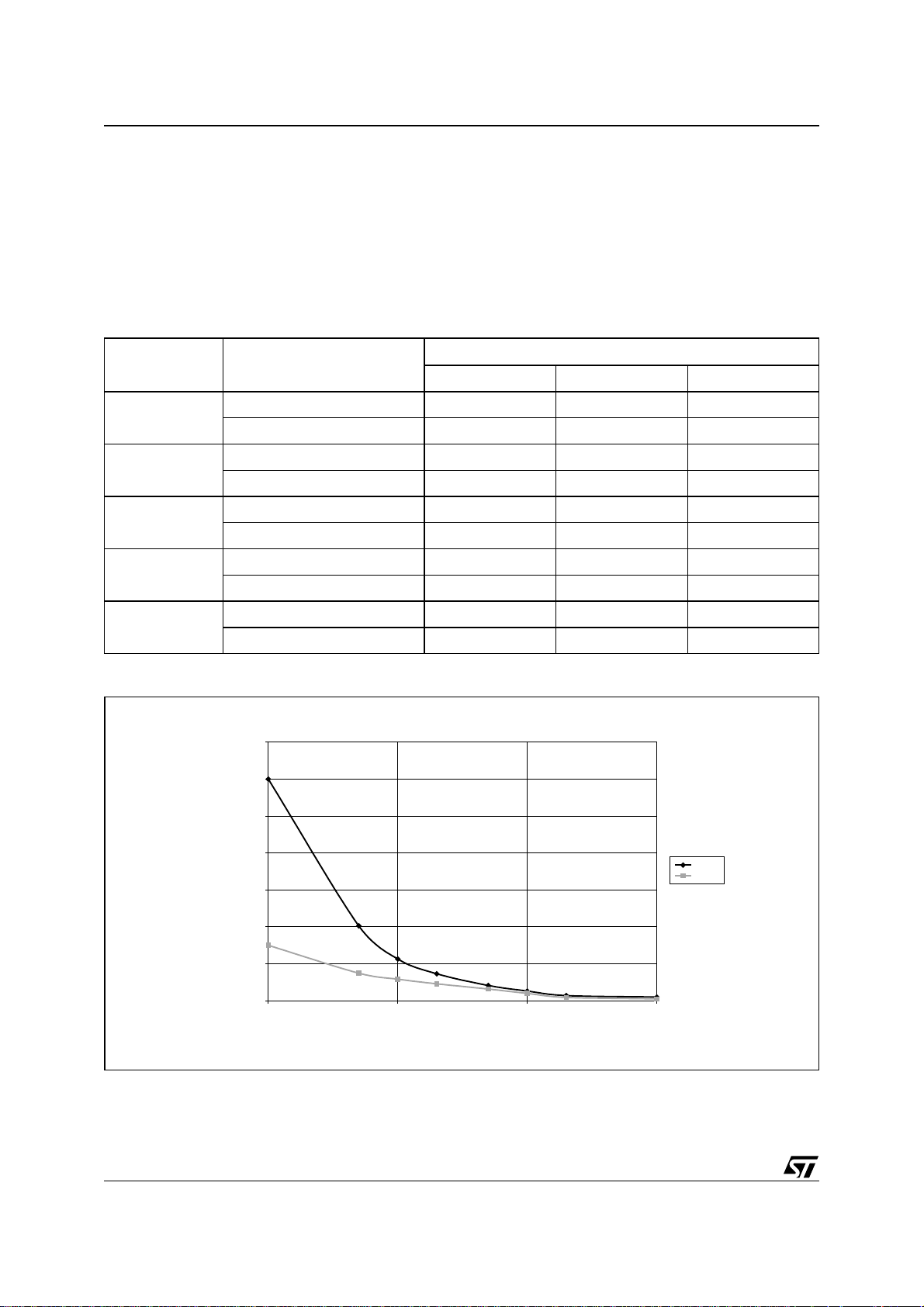
RESET THRESHOLDS
The STM8xx Reset Circuit devices have different reset threshold levels. Table 1, lists the thresholds,
, for each device and each temperature range.
V
RST
When considering the threshold level required for an application, it is also necessary to consider the maximum transient duration, not c ausing a reset pulse, with respect to voltage thresh old overdrive. A large
transient voltage overdrive need s less time to g enerate the Reset pulse, than a s mall transient voltage
overdrive, which needs much longer. Refer to the characterization graph shown in Figure 1.
Table 1. Reset Thresholds
V
(V)
Part Temperature Range (°C)
Min Typ Max
25 4.54 4.63 4.72
STM8xxL
-40 to 80 4.50 4.75
25 4.30 4.38 4.46
STM8xxM
-40 to 80 4.25 4.50
25 3.03 3.08 3.14
STM8xxT
-40 to 80 3.00 3.15
RST
STM8xxS
25 2.88 2.93 2.98
-40 to 80 2.85 3.00
25 2.58 2.63 2.68
STM8xxR
-40 to 80 2.55 2.70
Figure 1. Max Transient Duration NOT Causing Reset Pulse vs. Reset Comparator Overdrive
700.00
600.00
500.00
400.00
300.00
200.00
100.00
Maximum Transient Duration (µs)
0.00
1 10 100 1000
Reset Comparator Overdrive, V
– VCC (mV)
RST
AI07883
R/S/T
L/M
2/8
AN1790 - APPLICATION NOTE
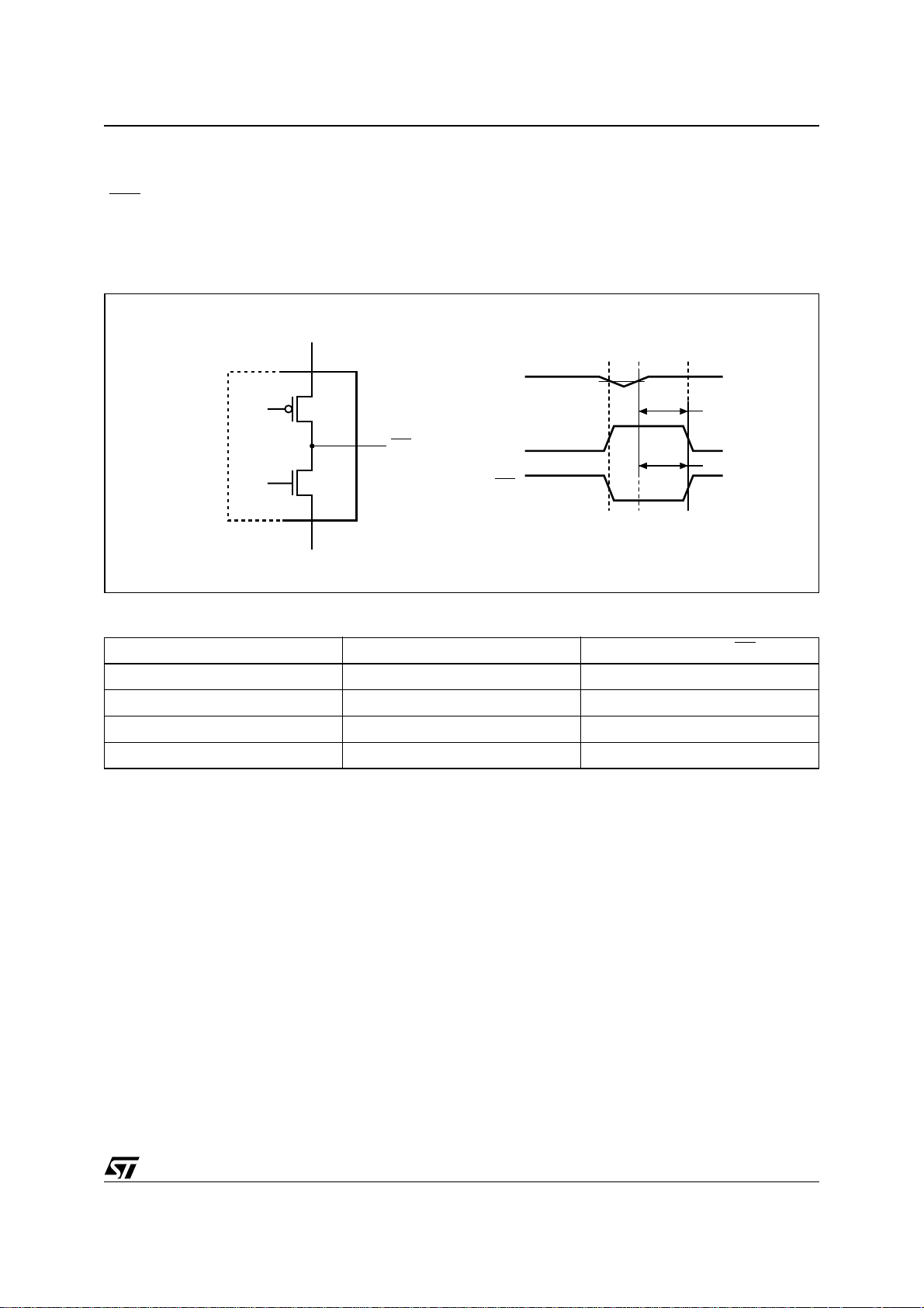
RESET OUTPUT
ST Reset Circuits feature a push-pull Reset out put with t he opt ion of an ac tive High (RST ) or ac tive Low
) output (see F igure 2 and Table 2). The push-pull output minimi zes the external c onnections be-
(RST
tween the Reset Circuit and the microprocessor or other logic devices. It offers high speed, almost rail-torail response, and the capability to source or sink current.
Figure 2. Reset Output
V
CC
V
CC
V
RST
trec
Reset Circuit
Table 2. Device Options
Part Reset Output active Manual Reset (MR)
STM809 Low No
STM810 High No
STM811 Low Yes
STM812 High Yes
RST/RST
V
SS
RST
trec
RST
AI08632
3/8

AN1790 - APPLICATION NOTE
MANUAL RESET INPUT
The STM811 and SMT812 devices fea ture a Manual Reset (MR
for a predefined time, t
and VSS (ground), as shown in Figure 3.
MR
. The simplest way to use this feature is to connect a push-button between the
rec
The Manual Reset has an internal 20 kΩ pul l-up resistor and a debounce circuit, which solves the problem
of any noise generated by switching the push-button.
The timing diagram represented in Figure 4 shows how the Manual Reset input functions. When MR
driven Low, the Reset (RST or RST
ing the time that MR
is Low. When the switch is released, MR goes High (thanks to the internal pull-up
) output becomes active after a delay of t
resistor), but the Reset output remains active for a time of t
The minimum pulse width of the M R
the M R
of MR
pulse width is shorter than t
, which can lead to the system not functioning correctly.
signal (t
MLMH(min)
MLMH(min)
, the RST/RST pulse generated is equal to the pulse width
= 10µs) must be taken into account in a design. If
Figure 3. Manual Reset Connection
V
CC
) input, which activates the Reset output
, and remains active dur-
MLRL
.
rec
is
Push-button
Reset
Figure 4. Manual Reset Waveform
MR
tMLRL
(1)
RST
tMLMH
Note: 1. RST for STM 810/812
2. Refer to STM 8xx datasheet for the tim i ng values .
MR
V
CC
RST
V
SS
trec
V
RESET
Input
V
CC
Microprocessor
SS
AI08637
AI08640
4/8

AN1790 - APPLICATION NOTE
CONNECTING THE RESET CIRCUITS IN AN APPLICATION
The standard connection of the Reset devices is very simple, as normally no other circuits are required.
The standard connections for the STM809, STM810, STM811 and STM812 are shown in Figure 5.
Figure 5. Standard Reset Device Connections
STM810 Connection STM809 Connection
V
CC
V
CC
V
CC
V
CC
V
CC
V
CC
V
CC
Push-button
Reset
MR
STM810
RST
V
SS
RESET
Input
V
Microprocessor
SS
STM809
RST
V
SS
RESET
Input
V
Microprocessor
SS
STM811 ConnectionSTM812 Connection
V
CC
V
CC
V
CC
STM812
RST
V
SS
RESET
Input
V
Microprocessor
SS
Push-button
Reset
MR
V
CC
STM811
RST
V
SS
V
RESET
Input
V
CC
Microprocessor
SS
AI08633
5/8

AN1790 - APPLICATION NOTE
Connection in a Noisy Environment
The internal debounce circuit in the ST Reset devices is especially designed to remove any noise generated by switching the push-button at the Manual Reset input. However the internal debounc e circuit may
not be sufficient to filter external noise in extremely noisy environments, for example, long wires in a noisy
environment or high speed buses near the Manual Reset input. In such cases, an external capacitor can
be added to solve the problem (see Figure 6). The recommended value of the capacitor is 0.1µF.
Figure 6. Reset Device Connection in a Noisy Environment
V
CC
V
RESET
Input
V
CC
Microprocessor
SS
AI08634
Push-button
Reset
C = 0.1µF
MR
V
CC
STM812
RST
V
SS
Connection to a Bi-directional Microprocessor Reset
Sometimes designers need to connect a Reset Circuit device to a m icroprocessor’s bi -directional Reset
input. In this case a resistor should be connected between the RST
output and the microprocessor’s RESET inp ut. T he va lue o f the resisto r s hould be high enough to lim it the c urrent when the microprocess or
pulls down the RESET
input and low enough to respond when RST goes low. The recomm ended value
of the resistor is 4.7kΩ (see Figure 7).
Figure 7. Reset Device Connection to a Bi-directional Microprocessor Reset
to other devices
V
CC
6/8
V
CC
STM809
RST
V
SS
R = 4.7kΩ
V
RESET
Input
V
CC
Microprocessor
SS
AI08635

AN1790 - APPLICATION NOTE
Connection With Reset Output V alid Dow n t o VCC = 0V
When V
circuit. In most applications this is not a problem, as most microprocessors do not operate below 1V. However, in applications where RST
the R ST
be small enough to pull the output to ground. The recommended value of the resistor is 100kΩ (see Figure
8).
falls bel ow 1V , th e RS T (S TM809/811) output no longer sinks curren t, but becomes a n open
CC
must be valid d own to 0V, a pull-down resi stor shou ld b e added to hold
output Low. The value of the resistor must be large enough not to load the RST outpu t, and still
Figure 8. Reset Device Connection With RST
V
CC
V
CC
RST
V
SS
Valid Down to VCC = 0V
STM809
R=100kΩ
V
RESET
Input
V
CC
Microprocessor
SS
AI08636
CONCLUSION
ST Reset Circuits are low-power supervisory devices, that have been specifically designed to monitor
power supplies in microprocessor systems.
In standard applications, they can be directly connec ted to the mi croprocessor, as no other ext ernal circuits are required. However, they can also be used in specific application environments, with the simple
addition of a resistor or capacitor.
They are available in small SOT23 and SOT143 packages; they require only a low supply current, typically
in the 5-10 µA range and offer a wide range of voltage thresholds.
REFERENCES
■ STM809, STM810, STM811, STM812 datasheet
REVISION HIST ORY
Table 3. Document Revision History
Date Version Revision Details
04-Dec-2003 1.0 First Issue.
7/8

AN1790 - APPLICATION NOTE
s
d
t
t
If you have any questions or suggestion concerning the matters raised in this document please send them
to the following electronic mail address:
ask.memory@st.com (for general enquiries)
Please remember to include your name, company, location, telephone number and fax number.
Information furnished is believed to be accurate and reliable. However, STMicroelectronics assumes no responsibility for the consequence
of use of such information nor for any infringement of patents or other rights of third parties which may result from its use. No license is grante
by implic ation or o th erwise u nder any pat ent or pat ent righ ts of STMicroelectron i cs. Specifications m entioned i n this publication are sub j ec
to change without notice. This publication supersedes and replaces all information previously supplied. STMicroelectronics products are no
authoriz ed for use as cri tical comp onents in lif e support dev i ces or systems witho ut express writ ten approv al of STMicro el ectronics.
The ST logo is a registered trademark of STMicroelectronics.
All other nam es are the pro perty of thei r respect ive owners
© 2003 STMi croelectronics - All ri ghts reser ved
STMicroelectron ics GROUP OF COMPANIES
Australi a - Belgium - Brazil - Ca nada - China - Czech Rep ubl i c - Finland - F rance - Germany - Hong Kong - India - Israel - Italy - Japan -
Malaysia - M al ta - Moroc co - Singapore - Spain - Sweden - Switzerlan d - United Ki ngdom - United States
www.st.com
8/8
 Loading...