


Conversion Guide, uPSD3200 to uPSD3400 series
1 Introduction
The uPSD family currently consists of three series , uPSD3200, uPSD3300, and uPSD3400.
All three series are available in the same kind of packages (52-pin and 80-pin TQFP), but
there are a few differences in pin definitions. This document describes the differences and
suggests methods to easily migrate designs from the uPSD3200 series to uPSD3400. You
can implement simple techniques on y our printed circuit b oard to accept either a uPSD3200
or a uPSD3400 during manufacturing. Please see Application Note AN1724 for similar
information regarding migrating d esigns from the uPSD3200 series to the uPSD3300 series ,
and see AN1773 for migrating from uPSD3300 to uPSD3400 designs.
Pin differences will be presented two categories:
■ Mandatory pin function changes for all applications, and
■ Conditional pin function changes depending on the application.
AN1787
Application note
There are also differences in SFRs and interrupt vectors, which may impact firmware
depending on the application. These differences are identified to help you migrate your
firmware.
For simplicity, the uPSD3200 series will be referred in this document as 3200, and the
uPSD3400 series will be referred to as 3400.
May 2007 Rev 2 1/27
www.st.com

Contents AN1787
Contents
1 Introduction . . . . . . . . . . . . . . . . . . . . . . . . . . . . . . . . . . . . . . . . . . . . . . . . 1
1.1 Summary of differences . . . . . . . . . . . . . . . . . . . . . . . . . . . . . . . . . . . . . . . 4
1.1.1 MCU Core Voltage . . . . . . . . . . . . . . . . . . . . . . . . . . . . . . . . . . . . . . . . . . 4
1.1.2 MCU Core . . . . . . . . . . . . . . . . . . . . . . . . . . . . . . . . . . . . . . . . . . . . . . . . 4
1.1.3 PWM . . . . . . . . . . . . . . . . . . . . . . . . . . . . . . . . . . . . . . . . . . . . . . . . . . . . 4
1.1.4 ADC . . . . . . . . . . . . . . . . . . . . . . . . . . . . . . . . . . . . . . . . . . . . . . . . . . . . . 4
1.1.5 LVD . . . . . . . . . . . . . . . . . . . . . . . . . . . . . . . . . . . . . . . . . . . . . . . . . . . . . 4
1.1.6 Watchdog . . . . . . . . . . . . . . . . . . . . . . . . . . . . . . . . . . . . . . . . . . . . . . . . . 4
1.1.7 I/O characteristics . . . . . . . . . . . . . . . . . . . . . . . . . . . . . . . . . . . . . . . . . . 4
1.1.8 USB . . . . . . . . . . . . . . . . . . . . . . . . . . . . . . . . . . . . . . . . . . . . . . . . . . . . . 4
1.1.9 UART and I2C . . . . . . . . . . . . . . . . . . . . . . . . . . . . . . . . . . . . . . . . . . . . . 5
1.1.10 DDC . . . . . . . . . . . . . . . . . . . . . . . . . . . . . . . . . . . . . . . . . . . . . . . . . . . . . 5
1.2 Summary of new uPSD3400 functions . . . . . . . . . . . . . . . . . . . . . . . . . . . 5
1.2.1 USB . . . . . . . . . . . . . . . . . . . . . . . . . . . . . . . . . . . . . . . . . . . . . . . . . . . . . 5
1.2.2 MCU Core . . . . . . . . . . . . . . . . . . . . . . . . . . . . . . . . . . . . . . . . . . . . . . . . 5
1.2.3 MCU core timing . . . . . . . . . . . . . . . . . . . . . . . . . . . . . . . . . . . . . . . . . . . 5
1.2.4 MCU core data pointers . . . . . . . . . . . . . . . . . . . . . . . . . . . . . . . . . . . . . . 5
1.2.5 SPI . . . . . . . . . . . . . . . . . . . . . . . . . . . . . . . . . . . . . . . . . . . . . . . . . . . . . . 5
1.2.6 ADC . . . . . . . . . . . . . . . . . . . . . . . . . . . . . . . . . . . . . . . . . . . . . . . . . . . . . 6
1.2.7 IrDA . . . . . . . . . . . . . . . . . . . . . . . . . . . . . . . . . . . . . . . . . . . . . . . . . . . . . 6
1.2.8 PCA . . . . . . . . . . . . . . . . . . . . . . . . . . . . . . . . . . . . . . . . . . . . . . . . . . . . . 6
1.2.9 JTAG debug . . . . . . . . . . . . . . . . . . . . . . . . . . . . . . . . . . . . . . . . . . . . . . . 6
1.2.10 Debug . . . . . . . . . . . . . . . . . . . . . . . . . . . . . . . . . . . . . . . . . . . . . . . . . . . 6
1.2.11 MCU clock . . . . . . . . . . . . . . . . . . . . . . . . . . . . . . . . . . . . . . . . . . . . . . . . 6
1.2.12 MCU clock division . . . . . . . . . . . . . . . . . . . . . . . . . . . . . . . . . . . . . . . . . . 6
1.2.13 Cross-Bar I/O . . . . . . . . . . . . . . . . . . . . . . . . . . . . . . . . . . . . . . . . . . . . . . 6
1.2.14 High Current I/O . . . . . . . . . . . . . . . . . . . . . . . . . . . . . . . . . . . . . . . . . . . . 6
1.2.15 5V-tolerant I/O . . . . . . . . . . . . . . . . . . . . . . . . . . . . . . . . . . . . . . . . . . . . . 7
2 Pin definitions . . . . . . . . . . . . . . . . . . . . . . . . . . . . . . . . . . . . . . . . . . . . . . 8
3 Mandatory pin changes . . . . . . . . . . . . . . . . . . . . . . . . . . . . . . . . . . . . . 12
3.1 52-pin Devices . . . . . . . . . . . . . . . . . . . . . . . . . . . . . . . . . . . . . . . . . . . . . 12
3.2 80-pin devices . . . . . . . . . . . . . . . . . . . . . . . . . . . . . . . . . . . . . . . . . . . . . 13
2/27

AN1787 Contents
4 PC layout suggestions . . . . . . . . . . . . . . . . . . . . . . . . . . . . . . . . . . . . . . 14
5 Conditional pin changes . . . . . . . . . . . . . . . . . . . . . . . . . . . . . . . . . . . . . 17
5.1 PWM . . . . . . . . . . . . . . . . . . . . . . . . . . . . . . . . . . . . . . . . . . . . . . . . . . . . . 17
5.2 52-pin devices . . . . . . . . . . . . . . . . . . . . . . . . . . . . . . . . . . . . . . . . . . . . . 17
5.3 80-pin devices . . . . . . . . . . . . . . . . . . . . . . . . . . . . . . . . . . . . . . . . . . . . . 17
5.4 PC Layout Suggestion for PWM . . . . . . . . . . . . . . . . . . . . . . . . . . . . . . . . 18
5.5 ADC, reassigned ADC channel numbers . . . . . . . . . . . . . . . . . . . . . . . . . 18
5.6 ADC voltage scaling . . . . . . . . . . . . . . . . . . . . . . . . . . . . . . . . . . . . . . . . . 19
5.7 ADC reference voltage . . . . . . . . . . . . . . . . . . . . . . . . . . . . . . . . . . . . . . . 19
5.8 LVD . . . . . . . . . . . . . . . . . . . . . . . . . . . . . . . . . . . . . . . . . . . . . . . . . . . . . . 20
6 Special function register (SFR) differences . . . . . . . . . . . . . . . . . . . . . 22
7 Interrupt vector differences . . . . . . . . . . . . . . . . . . . . . . . . . . . . . . . . . . 24
8 Conclusion . . . . . . . . . . . . . . . . . . . . . . . . . . . . . . . . . . . . . . . . . . . . . . . . 25
9 Revision history . . . . . . . . . . . . . . . . . . . . . . . . . . . . . . . . . . . . . . . . . . . 26
3/27

1.1 Summary of differences
1.1.1 MCU Core Voltage
The 3400 MCU core requires a 3.3V supply, even when used in a 5V system. This means
two separate supplies (5V V
supply (3.3V V
V
supply, which is 5V VCC for 5V devices, or 3.3V VCC for 3.3V devices.
CC
1.1.2 MCU Core
The 3200 MCU requires 12 clocks per instruction but t he 3400 uses just 4 clocks. The 3400
does not have an optional 12-clock operation mode. No modifications are needed to 3200
firmware for standard 8032 functions unless timing was established with software loops.
Modifications ARE required for firmware controlling some peripherals when migrating to
3400.
1.1.3 PWM
The five 8-bit PWM channels of the 32 00 are implemented with the Programmable Counter
Array (PCA) in the 3400, which has six 16-bit timer/counter modules. There are new SFRs,
and some PWM pin number assignments have changed on the 3400.
) is required for a 3.3V system. In contrast, 3200 devices use only a single
CC
and 3.3V VCC) are required in a 5V system, but just one
DD
AN1787
1.1.4 ADC
The four 8-bit ADC channels of the 3200 are imple mented using f our of the eigh t 10-bit ADC
channels on the 3400. There are new SFRs, but there are no ADC input pin number
changes. The ADC reference voltage (V
devices and V
have an ADC V
voltage on any 3400 ADC input or reference is V
is shared internally with the 3.3V VCC core supply . 80-pin 3400 devices do
REF
pin, and its maximum input voltage is V
REF
1.1.5 LVD
Both 5V and 3.3V 3400 devices have Low-Voltage Detect (LVD) trip point set for the 3.3V
V
supply level (2.5V). This must be considered when designing 5V systems.
CC
1.1.6 Watchdog
The watchdog timer is enabled after reset on 3200 devices, but it is disabled after reset on
3400 devices.
1.1.7 I/O characteristics
The 3.3V 3400 devices have 5V tolerant I/O on ports 3, and 4, but ports A,B,C, and D are
not 5V tolerant. The 3.3V 3200 devices do not have any 5V tolerant I/O ports.
1.1.8 USB
) input pin is not available on 52-pin 3400
REF
(3.3V). The maximum input
(3.3V) even in a 5V system.
CC
CC
The 3200 supports low-speed USB 1.1 (1.5Mbps), the 3400 supports full-speed USB 2.0
(12Mbps). The 3400 has all new SFRs for the USB channel. Some USB bus pin numbers
have changed between the 3200 and 3400.
4/27

AN1787
1.1.9 UART and I2C
Minor changes to SFR definitions.
1.1.10 DDC
No DDC interface is on the 3400.
1.2 Summary of new uPSD3400 functions
Listed below are new functions on the 3400 that were no t available on the 3300:
1.2.1 USB
The 3400 supports USB 2.0 Full-Speed (12Mbps) and includes the USB physical interface.
There are a total of 5 pair of endpoints (each pair consists of In and Out ). One endpoint pa ir
is for USB Control transfer types, the remaining four endpoint pairs can be used for any
combination of USB Interrupt or USB Bulk transfer types . Each individual e ndpoint has a 64byte FIFO (10 FIFOs total) to maintain USB data throughput.
1.2.2 MCU Core
The 8032 MCU core of the 3400 operates on 4-clo cks per in struction, with a maximum cloc k
rate of 40MHz, yielding 10 MIPS (Million Instructions Per Second) maximum performance
for single-byte instructions. The 3400 MCU core has a 16-bit internal path from memory to
enhance performance, meaning that double-byte instructions are fetched in a single MCU
cycle, which pushes average performance close to the peak performance. No firmware
changes are required to take advantage of this enhancement. In summary, 3400 has 10
MIPS peak performance, but you can e xpect about 9 MIPS a ver age perf ormance, compared
to 3.3 MIPS peak and 3.0 MIPS average performance from the 3200.
1.2.3 MCU core timing
The 3400 Turbo MCU core has a six-deep instruction prefetch queue and a four-way
branching address cache to increase performance. Code in smaller localities operate very
fast. No special firmware is required to take advantage of the prefetch queue or branching
cache. Be aware that firmware timing loops will not be accurate because of the nondeterministic nature of pipeline and cache architecture. Please use one of the many
hardware timer modules to create timing functions, not firmware loops.
1.2.4 MCU core data pointers
The 3400 Turbo MCU core includes dual data pointers to speed data transfers of XDATA.
The pointers can auto-increment and auto-decrement, providing rapid data movement from
source to destination locations. The 3200 has one only data pointer.
1.2.5 SPI
An SPI bus master interface is provided on the 3400.
5/27

1.2.6 ADC
Eight 10-bit ADC inputs are provided, compared to only four 8-bit ADC inputs on the 3200.
1.2.7 IrDA
The 2nd UART channel supports IrDA protocol, which be connected directly to an IR
transceiver.
1.2.8 PCA
The Programmable Co unter Arra y unit has six 16-bit tim er/counter (TC) modules that can be
used for PWM, Capture/Compare, Timers, or Counters. Three of the six TC modules can
operate from one time base , and the ot her three TC modules can oper ate from another time
base if desired. These six TC modules are in addition to the standard th ree 16-bit time r units
inside the 8032 MCU core, bringing a total of nine 16-bit timer/counters. The 3200 provides
only the three standard 16-bit 8032 timers.
1.2.9 JTAG debug
The JTAG port now functions as a debug port in addition to In-System Programming (ISP).
This eliminates the need for conventional hardware In-Circuit Emulation (ICE) tools.
AN1787
1.2.10 Debug
The 3400 has a dedicated debug input/ output pin. As an output, it ca n signal that a specified
debug ev en t has occurred, as an input it can t rigger a debu g e v ent to begin (e .g., bre akpoint
or trace)
1.2.11 MCU clock
3.3V 3400 devices can be clocked up to 40MHz, unlike 3.3V 3200 with 24MHz maximum.
1.2.12 MCU clock division
The 8032 MCU clock can be divided internally for lower power operation. The MCU may
change the clock divider ratio on-the-fly using SFRs. This affects the MCU only, not
peripheral clocks.
1.2.13 Cross-Bar I/O
Peripheral functions on Port 1 are also av ailab le on P ort 4 (cross-bar s witch), pro viding more
flexibility. There is no need to sacrifice one peripheral function when two functions are
available on a single pin, just use the other port.
1.2.14 High Current I/O
Eight I/O pins on Port 4 are each capable of sinking or sourcing 10mA for both, 3.3V and
5.0V 3400. In contrast, 3.3V 3200 pins ar e cap able of sinking 4mA each, while the 5V 3200
can sink 8mA each.
6/27

AN1787
1.2.15 5V-tolerant I/O
The following pins are 5V tolerant on 3.3V, 52-pin 3400 devices: P1.1 through P1.7, P3.1
through P3.7, P4.1 through P4.7, and RESET_IN_.
On 3.3V, 80-pin 3400 devices, the following pins are also 5V tolerant: MCU_AD0 through
MCU_AD7, RD_, WR_, and _PSEN. In contrast, 3.3V 3200 devices had no 5V tolerant I/O
pins.
Note: PSD functions have NOT changed from the 3200 to 3400. These funct ions include PLD,
memory mapping, memory management (code space vs. data space, and pagin g), Flash
memories, SRAM memory, and PSD I/O. The wider 16-bit internal data path on the 3400
(compared to 8-bit path on 3200) is transparent to the user.
Please note the SRAM on the 3400 can not be configured to reside in code space.
7/27
Pin definitions AN1787
2 Pin definitions
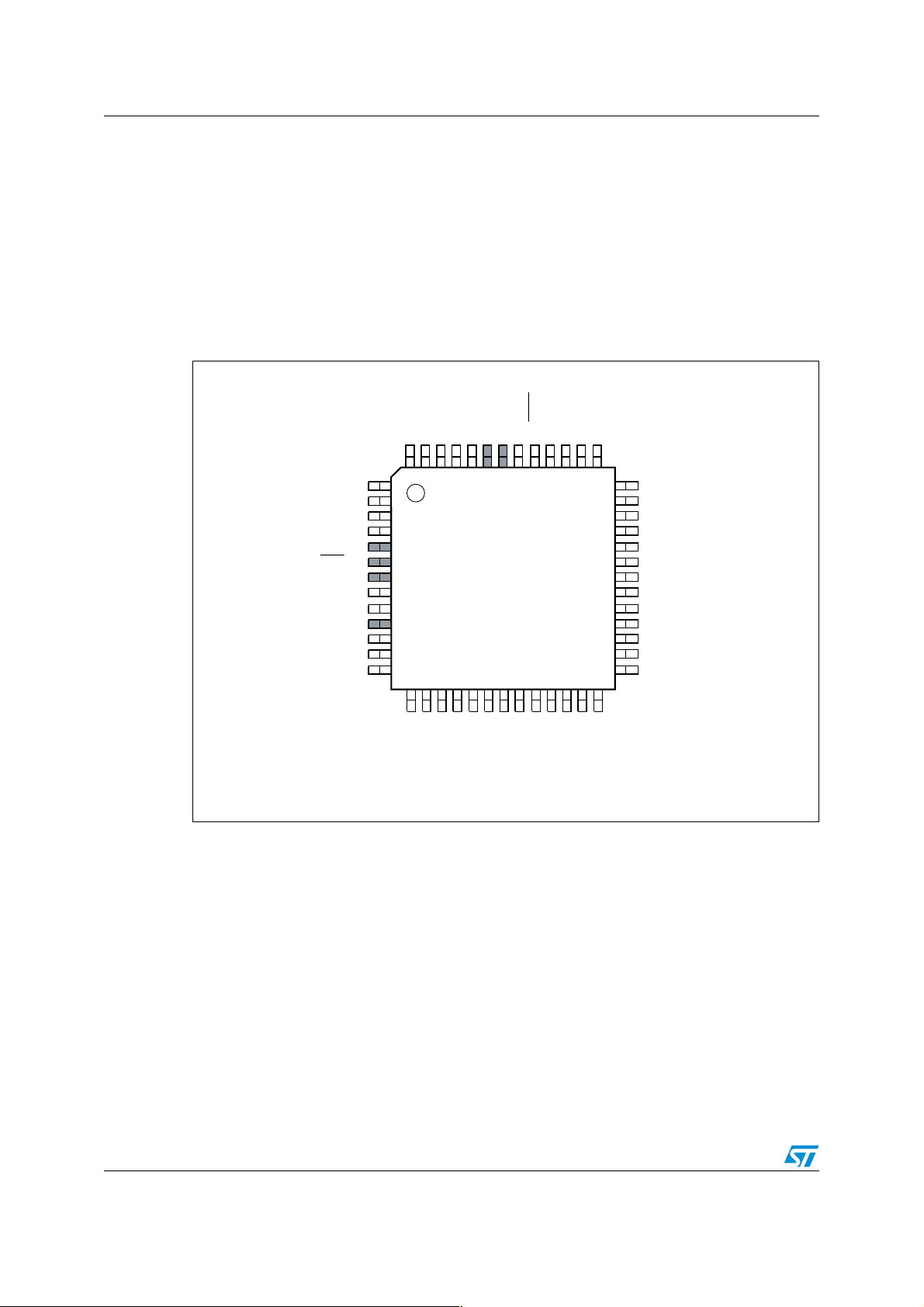
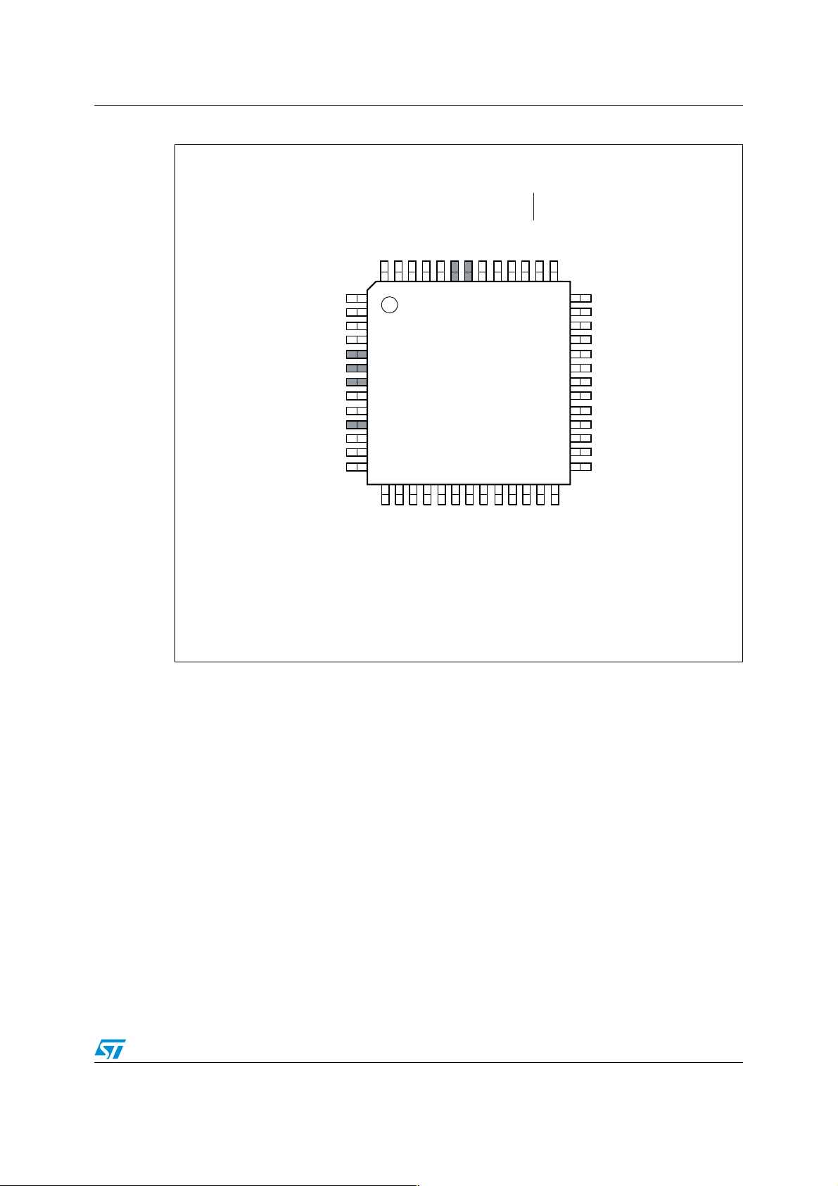
Figure 1 and Figure 2 show pin assignments of the 3200 and 3400 devices in both 52-pin
and 80-pin TQFP packages. Please see the 3200 and 3400 data sheets for detailed pin
function descriptions and physical dimensions of packages. Pins requiring mandatory
changes during migration are darkened in the figur es, this assume s that USB will be used in
both the 3200 and 3400 applications.
Note: 5V 3200 devices support USB while the 3.3V 3200 devices do NOT support USB.
Figure 1. uPSD3200 52-pin TQFP pin definition
REF
GND
RESET
PB6
PB7
P1.7/ADC3
PB0
PB1
PB2
PB3
PB4
PB5
V
52515049484746454443424140
P1.6/ADC2
PD1/CLKIN
PC7
JTAG TDO
JTAG TDI
USB–
PC4/TERR
USB+
V
GND
PC3/TSTAT
PC2/V
STBY
JTAG TCK
JTAG TMS
1
2
3
4
5
6
7
8
CC
9
10
11
12
13
14151617181920212223242526
P4.7/PWM4
P4.6/PWM3
P4.5/PWM2
P4.4/PWM1
uPSD32XX
52-pin TQFP
SYNC
GND
P4.3/PWM0
P4.1/DDC SCL
P4.2/DDC V
P3.1/TXD
P3.0/RXD
P4.0/DDC SDA
P3.2/EXINT0
P3.3/EXINT1
39 P1.5/ADC1
38 P1.4/ADC0
37 P1.3/TXD1
36 P1.2/RXD1
35 P1.1/T2X
34 P1.0/T2
33 V
CC
32 XTAL2
31 XTAL1
30 P3.7/SCL1
29 P3.6/SDA1
28 P3.5/T1
27 P3.4/T0
AI08885
8/27
AN1787 Pin definitions
Figure 2. uPSD3400 52-pin TQFP pin definition
/ADC6
/ADC7
(2)
RESET_IN_
PB6
PB7
(2)
P1.6/SPITXD
P1.7/SPISEL
(3)
REF
/V
CC
PB5
PB0
PB1
PB2
PB3
PB4
AV
GND
52515049484746454443424140
(1)
(2)
2
CSCL
2
CSDA
(2)
/ADC1
/ADC0
(2)
(2)
/ADC5
/ADC4
(2)
(2)
/ADC3
/ADC2
PD1/CLKIN
PC7
JTAG TDO
JTAG TDI
DEBUG
3.3V V
USB+
V
DD
GND
USB–
PC2/V
STBY
JTAG TCK
JTAG TMS
1
2
3
4
5
6
CC
7
(1)
8
uPSD34XX
52-pin TQFP
9
10
11
12
13
39 P1.5/SPIRXD
38 P1.4/SPICLK
37 P1.3/TXD1(IrDA)
36 P1.2/RXD1(IrDA)
35 P1.1/T2X
34 P1.0/T2
33 V
DD
32 XTAL2
31 XTAL1
30 P3.7/I
29 P3.6/I
28 P3.5/C1
27 P3.4/C0
14151617181920212223242526
GND
/TCM5/P4.6
/TCM4/P4.5
/TCM3/P4.4
(2)
(2)
(2)
/PCACLK1/P4.7
(2)
SPICLK
SPITXD
SPIRXD
SPISEL_
1. For 5V applications, VDD must be connected to 5.0V source. For 3.3V applications, VDD must be
connected to a 3.3V source.
/TCM2/P4.2
/TCM1/P4.1
(2)
(2)
/PCACLK0/P4.3
(2)
T2X
RXD1(IrDA)
TXD1(IrDA)
/TCM0/P4.0
(2)
T2
EXTINT0/TG0/P3.2
EXTINT1/TG1/P3.3
AI08887
TXD0/P3.1
RXD0/P3.0
2. These signals can be used on one of two different ports (Port 1 or Port 4) for flexibility. Default is Port 1.
3. V
and 3.3V AVCC are shared. ADC channels must use 3.3V as V
REF
for 52-pin package.
REF
9/27

Pin definitions AN1787
Figure 3. uPSD3200 80-pin TQFP pin definition
PD2
P3.3/EXINT
PD1
ALE
PC7
JTAG TDO
JTAG TDI
USB–
PC4/TERR
USB+
NC
V
GND
PC3/TSTAT
PC2/V
STBY
JTAG TCK
NC
P4.7/PWM4
P4.6/PWM3
JTAG TMS
PB0
P3.2/EXINT0
PB1
P3.1/TXD
PB2
P3.0/RXD
PB3
PB4
80797877767574737271706968676665646362
1
2
3
4
5
6
7
8
9
10
11
12
CC
13
14
15
16
17
18
19
20
21222324252627282930313233343536373839
PA7
PA6
PA5
P4.5/PWM2
P4.4/PWM1
PA4
P4.3/PWM0
uPSD32XX
80-pin TQFP
PA3
PB5NCV
SYNC
GND
P4.2/DDC V
REF
GND
RESET
PB6
PA2
PA1
P4.1/DDC SCL
P4.0/DDC SDA
PB7RDP1.7/ADC3
PA0
PSENWRP1.6/ADC2
AD0/P0.0
AD1/P0.1
AD2/P0.2
AD3/P0.3
61
40
P3.4/T0
60 P1.5/ADC1
59 P1.4/ADC0
58 P1.3/TXD1
57 P2.3/A11
56 P1.2/RXD1
55 P2.2/A10
54 P1.1/T2X
53 P2.1/A9
52 P1.0/T2
51 P2.0/A8
50 V
CC
49 XTAL2
48 XTAL1
47 P0.7/AD7
46 P3.7/SCL1
45 P0.6/AD6
44 P3.6/SDA1
43 P0.5/AD5
42 P3.5/T1
41 P0.4/AD4
AI08886
10/27

AN1787 Pin definitions
Figure 4. uPSD3400 80-pin TQFP pin definition
/ADC6
/ADC7
(2)
(2)
CC
PB0
P3.2/EXINT0/TG0
PB1
P3.1/TXD0
PB2
P3.0/RXD0
PB3
80797877767574737271706968676665646362
PB4
AV V
PB5
REF
V
GND
RESET_IN_
PB6
PB7RDP1.7/SPISEL
PSENWRP1.6/SPITXD
61
SPISEL_
SPITXD
P3.3/TG1/EXINT1
PD2
PD1
ALE
PC7
JTAG TDO
JTAG TDI
DEBUG
PC4/TERR
3.3V V
USB+
V
DD
GND
USB–
PC3/TSTAT
PC2/V
STBY
JTAG TCK
(2)
/PCACLK1/P4.7
(2)
/TCM5/P4.6
JTAG TMS
1
2
3
4
5
6
7
8
9
10
CC
11
(1)
12
uPSD34XX
80-pin TQFP
13
14
15
16
17
18
19
20
21222324252627282930313233343536373839
PA5
PA7
PA6
/TCM4/P4.5
(2)
SPIRXD
PA4
/TCM3/P4.4
(2)
/PCACLK0/P4.3
(2)
SPICLK
PA3
GND
/TCM2/P4.2
(2)
PA2
/TCM1/P4.1
(2)
(2)
T2X
PA1
PA0
/TCM0/P4.0
T2
MCU AD0
MCU AD1
MCU AD2
MCU AD3
60 P1.5/SPIRXD
59 P1.4/SPICLK
58 P1.3/TXD1(IrDA)
57 NC
56 P1.2/RXD1(IrDA)
55 NC
54 P1.1/T2X
53 NC
52 P1.0/T2
51 NC
50 V
49 XTAL2
48 XTAL1
47 MCU AD7
46 P3.7/I
45 MCU AD6
44 P3.6/I
43 MCU AD5
42 P3.5/C1
41 MCU AD4
40
P3.4/C0
(2)
/ADC5
(2)
/ADC4
(2)
/ADC3
(2)
/ADC2
(2)
/ADC1
(2)
/ADC0
(1)
DD
2
CSCL
2
CSDA
RXD1(IrDA)
TXD1(IrDA)
AI08888
1. For 5V applications, VDD must be connected to 5.0V source. For 3.3V applications, VDD must be
connected to a 3.3V source.
2. These signals can be used on one of two different ports (Port 1 or Port 4) for flexibility. Default is Port 1.
11/27

Mandatory pin changes AN1787
3 Mandatory pin changes
There are some pin changes (see Table 1 and Table 2) that are absolutely re q uir ed whe n
migrating from the 3200. These changes are a result of the additional voltage source
required by the 3400 MCU core and the reassignment of USB pins , which ar e highlighted as
dark colored pins in Figure 1 though Figure 4. It is assumed that USB was used in the 3200
and will be used in the 3400 design.
Note: 5V 3200 devices support USB while the 3.3V 3200 devices do NOT support USB.
3.1 52-pin Devices
Refer to Figure 1 and Figure 2.
● Pin 5
Pin 5 (USB–) on the 3200 must be pulled up to V
or not. The pull-up resistor value for 3.3V 3200 de vices is 2K Ω; the pull-up value f or 5V
3200 devices is 7.5KΩ.
Pin 5 on the 3400 device functions as a Debug input/output, and does not nee d a pullup to V
● Pins 6 and 10
The functions of pin 6 (PC4/TERR
CC
.
) and pin 10 (PC3/TSTAT) on 3200 devices have
been eliminated on the 52-pin 3400 devices to accommodate some pin function
reassignments. These two signals o n the 320 0 wer e used as general purpose I/O or as
optional JTAG ISP pins that reduce programming time.
Pin 6 on the 3400 is V
and must always be connected to a 3.3V VCC supply.
CC
Pin 10 on the 3400 is USB– and is connected to the USB bus for 3400 applications
(with no pull-up resistor).
● Pin 7
Pin 7 on both the 3200 and the 3400 is the USB+ signal and has not changed.
However, the 3200 supports low-speed USB, while the 3400 supports full-speed USB.
Low-speed USB requires a pull-up resistor on the USB– signal whereas the full-speed
USB requires a pull-up resistor on the USB+ signal for identification purposes. Since
3400 is full-speed, a pull-up resistor (1.5 KΩ) to 3.3V
should be in place on 3400 designs even if USB is not used.
● Pins 46 and 47
The functions of pins 46 and 47 have been swapped. Pin 47 on the 3400 must always
be connected to AV
The ADC V
(voltage reference) input was on pin 46 for the 3200, but is now on pin
REF
CC/VREF
.
47 for the 3400.
● V
CC
and V
DD
In a 3.3V system using a 3.3V 3400 device, pins 6, 8, 33, 47 must be connected to a
3.3V V
source.
CC
In a 5V system, using a 5V 3400 device, pins 6 and 47 should be connected to a 3.3V
V
source, and pins 8 and 33 should be connected to a 5.0V VDD source.
CC
● Pin 47 is dedicated to A/D Converter on the 3400 devices
, regardless of whether USB is used
CC
is required. This pull-up resistor
CC
12/27

AN1787 Mandatory pin changes
Table 1. 52-pin device changes
Pin 5 Pin 6 Pin 7 Pin 10 Pin 46 Pin 47
3200
3400 DEBUG 3.3V V
USB– (pull-
up)
PC4/TERR USB+ PC3/TSTAT ADC V
3.2 80-pin devices
Refer to Figure 3 and Figure 4. Table 2 summarizes the mandatory pin changes for 80-pin
devices.
● Pins 8
Pin 8 (USB–) on the 3200 must be pulled up to V
or not. The pull-up resistor value for 3.3V 3200 devices is 2KΩ, the p ull- up value for 5V
3200 devices is 7.5KΩ.
Pin 8 on 3400 devices functions as a Debug input/output, and does not need a pull up
to V
.
CC
● Pin 10
Pin 10 is the USB+ signal on 3200 de vices , b ut on 3400 it m ust alwa ys be con nected to
3.3V V
● Pin 11
Pin 11 on 3200 is not used, but on 3400 devices it is the USB+ signal and must be
pulled up to 3.3V V
● Pin 14
Pin 14 on 3200 is PC3/TSTAT which can be a general purpose I/O signal or an optional
JTAG ISP signal used to reduce programming time. If this signal was used in the 3200
design, you can connect it to pin 15 on the 3400 (not a mandatory signal).
Pin 14 on the 3400 is the USB– signal and is connected to USB bus (with no pull-up
resistor).
● Pins 16 and 17
Pin 16 on the 3200 is JTAG CLK used for ISP. Pin 16 on the 3400 is PC2/V
for general purpose I/O or for the battery input for SRAM backup. You will need to
reroute JTAG CLK to pin 17 on the 3400. JTAG CLK is a mandatory signal.
If PC2/V
PC2/V
● Pins 71 and 72
The functions of pins 71 and 72 have been swapped. Pin 72 on the 3400 must always
be connected to AV
● V
CC
In a 3.3V system using a 3.3V 3400 device, pins 10, 12, 50 must connect to 3.3V VCC
source.
In a 5V system, using a 5V 3400 device, pin 10 should be connected to a 3.3V V
source, and pins 12 and 50 should be connected to a 5. 0V V
● Pin 72 is dedicated to A/D Converter on 3400 devices.
CC
STBY
STBY
and V
.
(with 1.5KΩ) for USB identification purposes.
CC
was used in the 3200 design, you can connect it to pin 16 on the 3400.
is not a mandatory signal.
CC/VREF
DD
CC
USB+ (pull-
up)
REF
– PB5 AV
, regardless of whether USB is used
CC
CC/VREF
STBY
PB5
used
.
source.
DD
CC
13/27

PC layout suggestions AN1787
● Pin 51, 53, 55 and 57 are No Connect on 3400 devices. Address A8-A11 can be
brought out on PLD pins.
Table 2. 80-pin device changes
Pin 51,
Pin 8 Pin 10 Pin 11 Pin 14 Pin 16 Pin 17
53, 55, 57Pin 71 Pin 72
3200
USB–
(pull-up)
3400 DEBUG
USB+
3.3V
V
CC
No
Connect
USB+
(pull-up)
4 PC layout suggestions
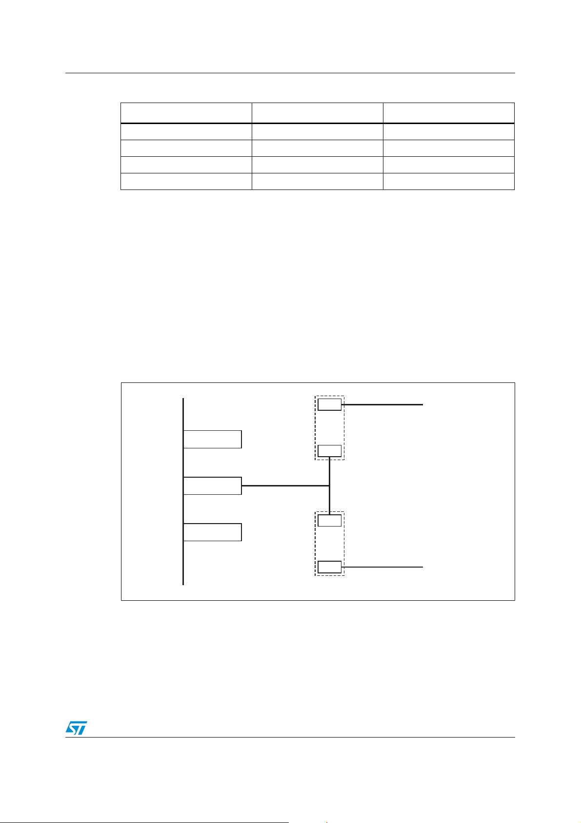
You can plan your printed circuit board layout in anticipation of migrating from the 3200 to
the 3400 by using simple and low cost techniques. One method involves the use of zeroohm resistors (either surface mount or thru-hole) and multiple circuit traces on the printed
circuit board. The idea is to install or not install these zero-ohm resistors at the time of board
manufacture, depending on which uPSD is installed.
For ex ample, Figure 5 shows how you can use this method to handle the swapped functions
of pins 46 and 47 on the 52-pin uPSD. In this example, resistors are installed at some
locations, and no resistors are installed at other locations as specified in Table 3.
A similar method can be used for an 80-pin device, using pins 71 and 72 instead of pins 46
and 47, respectively.
Figure 5. PC layout example for pin swapping
PC3/
TSTAT
USB–
JTAG
TCK
PC2/V
TBY
S
No
Connect
JTAG
TCK
A8-A11
No
Connect
No
Connect
PB5 AV
PB5
CC
uPSD
(52-pin)
Pin 47
Pin 46
R3
R4
14/27
R1
R2
R5
3.3V V
R6
PB5
V
REF
AI08892
CC

AN1787 PC layout suggestions
Table 3. 52-pin uPSD (0Ω) resistor installation example
R1 R2 R3 R4 R5 R6
3200 0Ω Blank Blank 0Ω Blank 0Ω
3400 Blank 0Ω 0Ω Blank 0Ω Blank
Figure 6 illustrates one way to handle the differing functions of Pins 5 through 10 on the 52-
pin uPSD. For this example, resistors are installed at some locations, and no resistors are
installed at other locations as specified in Table 4.
Note: The Deb ug signal is only for laboratory use and typically will be routed to a test point on the
circuit board.
Figure 6. PC Layout Example for 52-pin Devices
uPSD
(52-pin)
Pin 10
Pin 9
Pin 8
3.3V for 3400,
5.0V for 3200
GND
R3
R4
R1
PC3 / TSTAT
R2
USB–
1.5K
Pin 7
Pin 6
Pin 5
Table 4. 52-pin uPSD Resistor Installation Example (for Pins 5 through 10)
7.5K
R6
USB+
R5
PC4 / TERR
R7
DEBUG
AI08891
R1 R2 R3 R4 R5 R6 R7
3200 0Ω Blank 0Ω 7.5KΩ Blank 0Ω 0Ω
3400 Blank 0Ω 1.5KΩ Blank 0Ω Blank Blank
Figure 7 illustrates one way to handle the differing functions of pins 5 through 17 on the 80-
pin uPSD. For this example, resistors are installed at some locations, and no resistors are
installed at other locations as specified in the following Table 5.
Note: The Debug signal is only for laboratory use and typically will be routed to a test point
on the circuit board.
15/27

PC layout suggestions AN1787
Figure 7. PC layout example for 80-pin devices
uPSD
(80-pin)
Pin 17
R1
JT A G TCK
Pin 16
Pin 15
Pin 14
Pin 13
Pin 12
Pin 11
Pin 10
GND
1.5K
R9
R3
R5
R7
3.3V for 3400,
5.0V for 3200
R10
R8, 7.5K
R2
R4
R6
R11
R12
PC2 / V
STBY
PC3 / TSTAT
USB–
USB+
Pin 9
Pin 8
Table 5. 80-pin uPSD resistor installation example (for pins 5 through 17)
R1 R2 R3 R4 R5 R6 R7 R8 R9 R10 R11 R12 R13
3200 Blank 0Ω Blank
7.5
Blank 0Ω Blank 0Ω Blank Blank Blank 0Ω 0Ω
KΩ
3400 0Ω Blank 0Ω Blank 0Ω Blank 0Ω Blank
16/27
R13
1.5
0Ω 0Ω Blank Blank
KΩ
PC4/TERR
DEBUG
AI08890

AN1787 Conditional pin changes
5 Conditional pin changes
There are some pin changes that may or may not apply to your design, depending on your
application. These changes must be considered when migrating to the 3400 and you have
used the PWM or ADC peripherals of the 3200. There is also a conditional change
regarding the use of the Low-Voltage Detect (LVD) feature in 5V 3400 devices.
5.1 PWM
There are five PWM outputs on th e 3200, and six PWM outputs on the 3400. If y ou have
used any of PWM outputs PWM1, PWM2, or PWM3, on the 3200 then there are no pin
changes when migrating to the 3400. However, if you have used PWM outputs PWM0 or
PWM4 on the 3200, then you will have to connect to different pins on the 3400.
The Programmable Counter Array (PCA) on the 3400 has six Timer/Counter I/O pins,
labeled TCM0 through TCM5, that can be used for PWM outputs, and the PCA also has two
clock input pins labeled PCACLK0 and PCACLK1. These eight PCA pins are all on P ort 4. It
is the two PCA clock input pins of the 3400 that conflict with the PWM0 and PMW4 pin
assignments of the 3200.
5.2 52-pin devices
Refer to Figure 1 and Figure 2.
If you are using up to three of the five PWM outputs on the 3200, do not use output s PMW0
or PWM4. Instead, use outputs PWM1, PWM2, or PWM3 and there will be no pin conflicts
when migrating to the 3400.
If you are using f our or more PWM outputs on th e 3200, then PWM0 on pin 18, o r PWM4 on
pin 14, they will have to be moved to one of the following pins on the 3400: pins 15, 16, 17,
20, 21, or 22.
5.3 80-pin devices
Refer to Figure 3 and Figure 4.
If you are using up to three of the five PWM outputs on the 3200, do not use output s PMW0
or PWM4. instead, use outputs PWM1, PWM2, or PWM3 and there will be no pin conflicts
when migrating to the 3400.
If you are using f our or more PWM outputs on th e 3200, then PWM0 on pin 27, o r PWM4 on
pin 18, they will have to be moved to one of the following pins on the 3400: pins 19, 23, 25,
30, 31, or 33.
17/27

Conditional pin changes AN1787
5.4 PC Layout Suggestion for PWM
Figure 8 is an example of how to move PWM output PWM0 on a 3200 device to the PCA
output TCM2 on a 3400 device (52-pin). When a 3200 is installed, R1 is populated with a
zero-ohm resistor and R2 is blank. When a 3400 is installed, only R2 is popula ted. A similar
method can be used for an 80-pin device using pins 27 and 30 instead of pins 18 and 20,
respectively.
Figure 8. PC layout example to swap PWM outputs
uPSD
(52-pin)
R2
Pin 20
R1
Pin 18
5.5 ADC, reassigned ADC channel numbers
The 3200 has four ADC inputs (8-bit resolution), and the 3400 has eight ADC inputs (10-bit
resolution). The physical ADC input pin numbers have not been changed, but the logical
ADC channel numbers change when migrating from 3200 to 3400. This means no changes
to the PC board are required, but MCU firmware must change to account for different
channel numbers. Firmware changes must occur anyway because there are SFR changes,
identified in the next section. Table 6 refers to 52-pin uPSD devices and Table 7 refers to 80pin uPSD devices.
Table 6. Reassigned ADC Channel Numbers, 52-pin uPSD
Pin Number on 52-pin TQFP 3200 Device 3400 Device
38 ADC Channel 0 ADC Channel 4
39 ADC Channel 1 ADC Channel 5
40 ADC Channel 2 ADC Channel 6
PWM_out
AI08889
41 ADC Channel 3 ADC Channel 7
18/27
AN1787 Conditional pin changes
Table 7. Reassigned ADC Channel Number, 80-pin uPSD
Pin Number on 80-pin TQFP 3200 Device 3400 Device
59 ADC Channel 0 ADC Channel 4
60 ADC Channel 1 ADC Channel 5
61 ADC Channel 2 ADC Channel 6
64 ADC Channel 3 ADC Channel 7
5.6 ADC voltage scaling
For all 3400 devices, both 3.3V and 5V, the maximum input voltage level on any of the eight
ADC inputs is the MCU core voltage, V
are to be sampled in a 5V 3400 system, they must be scaled down t o 3.3V V
for 5V 3200 de vices, if 5V signals are sampled, they do not ha v e to be scaled down because
the maximum ADC input voltage is 5V Vcc (5.5V max).
Figure 9 illustrates one way to scale a 0-5V analog signal down to 0-3.3V when a 3400
device is used. For example, if a 3400 device is installed, resistor R1 is populated with a
332KΩ resistor, and R2 is populated with a 665KΩ resistor. Precision 1% resistors are
recommended. Alternately, if a 3200 is installed, R1 is populated with a zero-ohm resistor
and R2 is left blank because no scaling is needed.
(3.6V maximum). This means that if 5V signals
CC
. In contrast,
CC
Figure 9. Scaling 5V signal for 3.3V ADC Input
uPSD
ADC Input
5.7 ADC reference voltage
The maximum ADC Reference Voltage (V
V
(3.6V max), for both 3.3V and 5V 3400 devices. In contrast, f or 5V 3200 devices the
CC
maximum ADC reference voltage is 5V V
switch the source for V
populated with a zero-ohm resistor and R2 is blank. If a 5V 3400 is installed, only R2 gets
during manufacturing if needed. If a 5V 3200 is installed, R1
REF
ANALOG
INPUT,
0-5V Range
R1
R2
GND
AI08882
) allowed on the 3400 is the MCU core v oltage,
REF
(5.5V max). Figure 10 shows one method to
CC
19/27

Conditional pin changes AN1787
the zero-ohm resistor. This ONLY applies to 80-pin uPSD devices because 52-pin 3400
devices do not have a V
input as discussed in the MANDATORY PIN CHANGE section
REF
and in Figure 5.
Figure 10. Switching sources of V
5.8 LVD
The Low Voltage Detect (LVD) circuitry on all 3400 devices (both 3.3V and 5V) will generate
an internal reset signal whenever the MCU 3.3V V
fine for 3.3V systems using a 3.3V 3400 device. However, for 5V systems using a 5V 3400
device, it is recommended to use an external LVD circuit to drive the RESET_IN_ pin if it is
desired to monitor the 5.0V V
Regarding the 3200, there is no problem with 5V devices because the LVD circuitry has an
internal trip point at 4.0V.
uPSD
(80-pin)
Pin 70
ADC V
REF
in 80-pin uPSD devices
REF
5.0V V
for 3200
R1
R2
3.3V V
for 3300
AI08883
voltage level dips below 2.5V. This is
CC
system supply in addition to the 3.3V VCC supply.
DD
CC
CC
RESET_IN_ is an active-low, open-drain, 5V tolerant input. RESET_IN_ is located at pin 44
on 52-pin devices, or pin 68 on 80-pin devices.
Figure 11 illustrates a scheme that may be used when migr ating from a 5V 3200 de vice to a
5V 3400 device . In this e xample , R1 is populate d with a zero -ohm resistor only when a 3400
is installed, but R1 is left blank when a 3200 is used (supervisor device is optional when
3200 is used). R2 is always populated with a 10K resistor. Since the pin RESET_IN_ is
open-drain, it may be driven by multiple open-drain sources.
Suggestion: If a real-time cloc k (R TC) is needed in the system, choose an R TC that also has
an LVD reset output so you can use it as shown in Figure 11. There are many types of these
devices available from ST at www.st.com/nvram.
Note: An external LVD circuit is not needed for 3.3V 3400 devices in a 3.3V system.
20/27

AN1787 Conditional pin changes
Figure 11. Applying External LVD Circuit to 3400 5V System
uPSD
RESET_IN_
R2
10K
R1
5V
RESET_S_
RESET_J_ from
JTAG connector
RESET_B_ from
Push-button
Supervisor
Device or
discrete
LVD circuit
AI08884
21/27

Special function register (SFR) differences AN1787
6 Special function register (SFR) differences
The are a number of SFRs in the 3200 that ha ve changed compared to t he 3400. Ther e are
also a number of ne w SFRs in the 3400 t o control ne w peripherals a nd f eatures . None of th e
standard 8032 SFRs have changed (those defined in standard Intel 8032 archite cture).
Please see the full 3400 data sheet for a detailed description of new and changed SFRs.
Below is a summary of the differences for those SFRs that have changed functi on or
location (the SFRs with black background in Table 8). Please adjust your firmware for these
changes.
● 87: PCON
New POR Bit to determine source of last reset.
● 91: P3SF1
Used to be P1SF1. P1SF1, but it now has new meaning since it is linked to P4SF1
(please see the full 3400 data sheet).
● 96: ADAT1
Now different because 3400 has a 10-bit ADC, not an 8-bit ADC.
● 97: ACON
New bits to control ADC interrupt.
New bit to access eight ADC channels instead of four channels.
● A7/A8: ICA/IA
New Interrupt Enable bits for Debug, ADC, SPI, and PCA.
● B7/B8: IPA/IP
New Interrupt priority bits f or Debug, ADC, SPI, and PCA.
● D8/D9: SCON1/SBUF1
2nd UART control and data buffer. Same function as 3200, but new SFR address
location in 3400.
● DC: S1CON
STO and STA Bits do not have to be cleared by soft w are as they did in 3200. The 3400
has hardware (silicon) to assist, which improves I
overhead.
● DD: S1STA
More efficient use of INTR and ACK_REP_ Bits for I
● MANY USB SFRS
There are 19 new SFRs related to th e Full-Speed USB interface, all of which start with
the letter “U” and the CCON1 SFR.
2
C performance and reduces softw are
2
C.
Table 8 shows all the 3400 SFRs. Those with a black background and white letters indicate
3400 SFRs that have changed from the 3200 definition. Those with a gray background and
black letters are new SFRs in the 3400.
22/27
AN1787 Special function register (SFR) differences
Table 8. SFRs in the 3400
SFR
Addr
F8 CCON0 CCON1
(1)
(1)
USIZE
UIF2
F0 B UCON
(1)
E8 UIF0
UIF1
E0 ACC UADDR
D8 SCON1
(2)
SBUF1
(2)
(1)
SFR Register Name
(1)
CCON2 CCON3 FF
(1)
UBASEH
(1)
UPAIR
S1SETUP S1CON
UIF3
(1)
(1)
(1)
UBASEL
UCTL
UIE0
(1)
(1)
(2)
(1)
USCI
USTA
UIE1
S1STA
(1)
(1)
((1)
(1)
USCV
USEL
(1)
UIE2
(2)
S1DAT S1ADR DF
UIE3
(1)
(1)
D0 PSW SPICLKD SPISTAT SPITDR SPIRDR SPICON0 SPICON1 D7
C8 T2CON RCAP2L RCAP2H TL2 TH2 IRDACON DSTAT CF
C0 P4
B8 IP
B0 P3
A8 IE
(2)
(2)
CAP
COML3
CAP
COMH1
TCM
MODE0
A0 P2 PCACL0 PCACH0 PCACON0 PCASTA WDRST IEA
CAP
COMH3
CAP
COML4
CAP
COMH4
PCACL1 PCACH1 PCACON1
CAP
COML2
TCM
MODE1
CAP
COMH2
TCM
MODE2
PWMF0 IPA
CAP
COML0
CAP
COML5
TCM
MODE3
CAP
COMH0
CAP
COMH5
TCM
MODE4
WDTKEY
PWMF1 C7
TCM
MODE5
(2)
CAP
COML1
(2)
98 SCON0 SBUF0 BUSCON DIR DVR 9F
90 P1 P3SFS
(2)
P4SFS0 P4SFS1 ADCPS ADAT0 ADAT1
(2)
ACON
(2)
88 TCON TMOD TL0 TL1 TH0 TH1 P1SFS0 P1SFS1 8F
80 P0 SP DPL DPH DPTC DPTM PCON
1. New SFRs in uPSD3400
2. SFRs changed in uPSD3400
(2)
SFR
Addr
F7
EF
E7
BF
B7
AF
A7
97
87
23/27

Interrupt vector differences AN1787
7 Interrupt vector differences
There are new interrupt vectors for the 3400, an d some interrupt priority levels have
changed. See Table 9 for comparison of interrupt vectors of 3200 and 3400 and their relati ve
priorities. Please adjust your firmware accordingly.
Table 9. interrupt vector tables and priority
Interrupt Source 3400 Priority
JTAG Debug 0 (high) 0063 N/A N/A
External INT0 1 0003 0 0003
Timer 0 2 000B 2 000B
External INT1 3 0013 4 0013
Timer 1 4 001B 6 001B
UART0 5 0023 8 0023
Timer 2 + EXF2 6 002B 9 002B
SPI 7 0053 N/A N/A
USB 8 0033 7 0033
2
C 9 0043 3 0043
I
ADC 10 003B N/A N/A
PCA 11 005B N/A N/A
UART1 12 (low) 004B 1 004B
DDC N/A N/A 5 003B
3400 Vector
Address (hex)
3200 Priority
3200 Vector
Address (hex)
24/27

AN1787 Conclusion
8 Conclusion
The suggestions for methods to easily migrate designs from the uPSD3200 series to
uPSD3400 allow the user to implement firmware and software settings, as well as simple
techniques on the printed circuit board to accept either a uPSD3200 or a uPSD3400 during
manufacturing.
For current information on ST Flash uPSD products, please consult our pages on the world
wide web:
www.st.com/micropsd
For application support:
apps.psd@st.com (please include your name, company, location, telephone number, and
fax number)
25/27

Revision history AN1787
9 Revision history
Table 10. Document revision history
Date Revision Changes
26-Apr-2004 1 First Issue
14 -May-2007 2
Document reformatted.
Updated page 4, 6, 8,10, 11 and 12.
26/27

AN1787
Please Read Carefully:
Information in this document is provided solely in connection with ST products. STMicroelectronics NV and its subsidiaries (“ST”) reserve the
right to make changes, corrections, modifications or improvements, to this document, and the products and services described herein at any
time, without notice.
All ST products are sold pursuant to ST’s terms and conditions of sale.
Purchasers are solely res ponsibl e fo r the c hoic e, se lecti on an d use o f the S T prod ucts and s ervi ces d escr ibed he rein , and ST as sumes no
liability whatsoever relati ng to the choice, selection or use of the ST products a nd services described herein.
No license, express or implied, by estoppel or otherwise, to any intellectual property rights is granted under this document. If any part of this
document refers to any third pa rty p ro duc ts or se rv ices it sh all n ot be deem ed a lice ns e gr ant by ST fo r t he use of su ch thi r d party products
or services, or any intellectua l property c ontained the rein or consi dered as a warr anty coverin g the use in any manner whats oever of suc h
third party products or servi ces or any intellectual property contained therei n.
UNLESS OTHERWISE SET FORTH IN ST’S TERMS AND CONDITIONS OF SALE ST DISCLAIMS ANY EXPRESS OR IMPLIED
WARRANTY WITH RESPECT TO THE USE AND/OR SALE OF ST PRODUCTS INCLUDING WITHOUT LIMITATION IMPLIED
WARRANTIES OF MERCHANTABILITY, FITNESS FOR A PARTICUL AR PURPOS E (AND THEIR EQUIVALE NTS UNDER THE LAWS
OF ANY JURISDICTION), OR INFRINGEMENT OF ANY PATENT, COPYRIGHT OR OTHER INTELLECTUAL PROPERTY RIGHT.
UNLESS EXPRESSLY APPROVED IN WRITING BY AN AUTHORIZED ST REPRESENTATIVE, ST PRODUCTS ARE NOT
RECOMMENDED, AUTHORIZED OR WARRANTED FOR USE IN MILITARY, AIR CRAFT, SPACE, LIFE SAVING, OR LIFE SUSTAINING
APPLICATIONS, NOR IN PRODUCTS OR SYSTEMS WHERE FAILURE OR MALFUNCTION MAY RESULT IN PERSONAL INJ URY,
DEATH, OR SEVERE PROPERTY OR ENVIRONMENTAL DAMAGE. ST PRODUCTS WHICH ARE NOT SPECIFIED AS "AUTOMOTIVE
GRADE" MAY ONLY BE USED IN AUTOMOTIVE APPLICATIONS AT USER’S OWN RISK.
Resale of ST products with provisions different from the statements and/or technical features set forth in this document shall immediately void
any warranty granted by ST fo r the ST pro duct or serv ice describe d herein and shall not cr eate or exten d in any manne r whatsoever , any
liability of ST.
ST and the ST logo are trademarks or registered trademarks of ST in various countries.
Information in this document su persedes and replaces all information previously supplied.
The ST logo is a registered trademark of STMicroelectronics. All other names are the property of their respective owners.
© 2007 STMicroelectronics - All rights reserved
STMicroelectronics group of compan ie s
Australia - Belgium - Brazil - Canada - China - Czech Republic - Finland - France - Germany - Hong Kong - India - Israel - Italy - Japan -
Malaysia - Malta - Morocco - Singapore - Spain - Sweden - Switzerland - United Kingdom - United States of America
www.st.com
27/27
 Loading...