

Page 1
AN1783
Obsolete Product(s) - Obsolete Product(s) Obsolete Product(s) - Obsolete Product(s)
®
APPLICATION NOTE
HOW TO MAKE FIRE-WIRE COMMUNICATION PORT SAFE?
P. MERCERON
Video-mediaequipmentgrowthhasleadmanufacturers to use fasttransmission buses in orderto share information quickly and easily.
In many cases, video equipment use Fire-Wire link (IEEE1394) which brings the following features:
Up to 63 devices can be plugged on the bus
n
400Mb/s data transmission rate
n
Hot plugging
n
Power through the cable
n
Plug-and-play
n
Low cost cabling
n
Low implementation cost
n
As a matter of fact, this race for fast transmission and small compact video machines (cameras, mobiles,
videoequipment) has broughtmore and more integratedand sensitive electronicdevices at thesametime.
Asa result, on onehand, protection devices havebeen required tomakethe system morerobustregarding
ESD while, on the other hand, line adaptation have been implemented to prevent fastsignal distortion due
to high data rate transmission across non ideal elements.
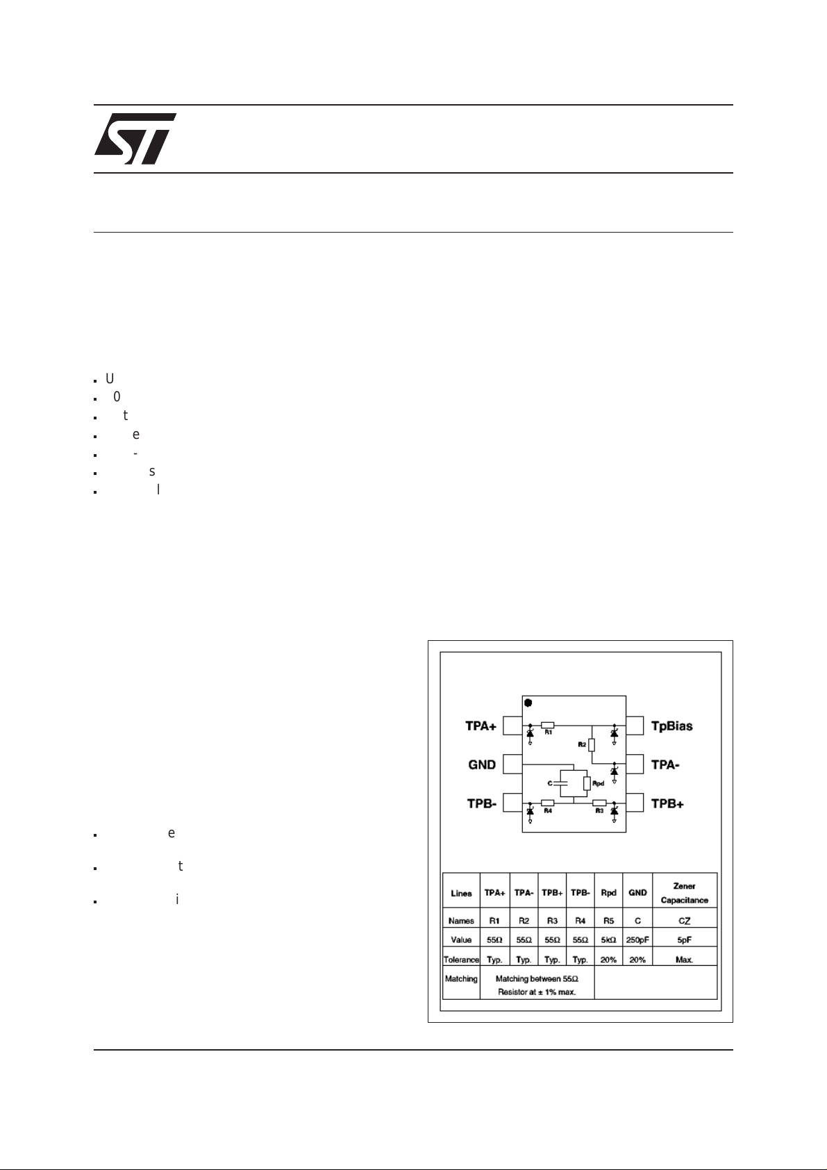
ST1394-01SC6 is one of those devices that com-
Fig. 1: ST1394-01SC6 internal diagram.
bine both ESD protection and line termination at a
time in one chip especially designed for Fire-Wire
transmission.
Its ± 4kV ESD IEC61000-4-2 compliance and
small package (1.5x2.8mm) makes it very convenient for IEEE1394 link.
The following internal diagram gives an idea of its
characteristics.
We can notice on
n
ESD protection is performed with clamping
figure 1
the following points:
diodes located at each line side.
n
RC elements realize line termination at each
data lines
n
Moreover, intrinsic clamping diode capacitors
offers RF rejection for GSM bandwidth.
October 2003 - Ed: 1
1/9
Page 2
Obsolete Product(s) - Obsolete Product(s) Obsolete Product(s) - Obsolete Product(s)
AN1783 - APPLICATION NOTE
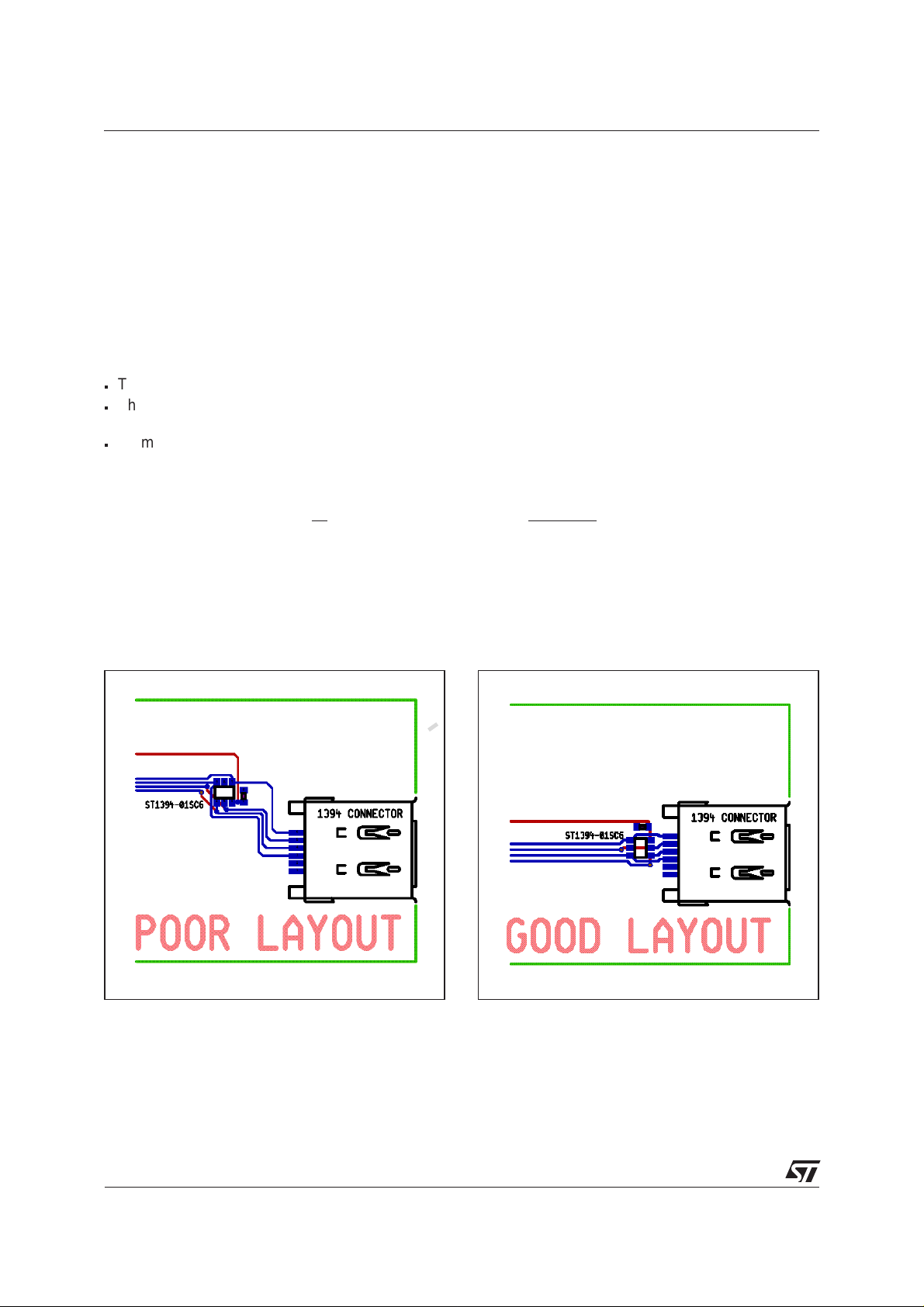
ST1394-01SC6 BOARD PLACEMENT RECOMMANDATIONS
Whatever the protection device at Fire Wire connector, it is known that upon ESD strike occurrence, a remaining over voltage is applied at sensitive IC side. In main cases a small part of this over voltage is coming from the clamping of the protection diode and a larger part from the copper track that connects
component altogether. For this reason it is important also to focus on the way component are routed.
Theway the ST1394-01SC6ismounted on theFire-Wire communication printedboardis also amajor concern. This will affect the ESD and line termination efficiency. Keep in mind when facing +4kV ESD surge
(IEC61000-4-2, level 2), a 10mm long; 0,5mn wide; 35µm thick copper track will induce about 70V!!
over-voltage due to track parasitic inductance.
Indeed, fast di/dt induced by the ESD IEC61000-4-2 level 2 brings the following calculation:
The ESD surge has a step rise time of 0.7ns minimum.
n
The level 2 of the ESD test table stands for 4kV air discharge and the internal series resistance of the
n
equivalent ESD generator is 330 ohms, thus the peak current induced by the 4kV surge is roughly 12A
A 1mm, 35µm thick, 0.5mm wide is 0.4nH
n
Then considering a 10mm; 35µm; 0.5mm copper track, the voltage drop along this track comes up with:
dI
=
; then it is
VV
=××
10 04 10
VL
dt
So shorter the tracks, better the ESD suppression.
.
−
9
07 10
.
121
.
×
−
9
=
70
!!
Next figures 2 and 3 give an idea of component placement on a printed circuit board:
Fig. 2: Bad layout. Fig. 3: Good layout.
2/9
Page 3
Obsolete Product(s) - Obsolete Product(s) Obsolete Product(s) - Obsolete Product(s)
AN1783 - APPLICATION NOTE
ESD PROTECTION
The ST1394-01SC6 complies with IEC61000-4-2 standard, level 2, air discharge surge test (± 4kV).
The next figure shows the way the ST1394-01SC6 is connected to Fire Wire communication port:
Fig. 4: ST1394-01SC6 connection diagram.
Fire Wire
communication
bus
{
When the surge is applied at the Fire-Wire communication port, the ST1394-01SC6 eliminates the
over-voltage like shown further:
The way it works!
UponESD occurrence (
Considering
V
= Z1; ST1394-01SC6 internal diode breakdown voltage
BR
R
= dynamic resistance =1Ω for ST1394-01SC6
d
That means the remaining over-voltage at the ST1394-01SC6 input line is 12V above Z1 diode breaking
voltage.
Fig. 5: ESD occurence.
IA
112≈
cf.fig. 5
(≈4000V/330Ω per IEC61000-4-2 level 2)
),Z1 diode clampsthe surge andtheremaining voltage atits terminations is:
VV RIV V
1112=+×≡+
BR d BR
Vcc
I1
V1
Z1
IC to
protect
ESD surge
I1
V1
3/9
Page 4

Obsolete Product(s) - Obsolete Product(s) Obsolete Product(s) - Obsolete Product(s)
AN1783 - APPLICATION NOTE
WHAT HAPPENS IN A PRACTICAL CASE?
Fig. 6: Test set-up picture.
Fig. 7: Remaining over voltage at ST1394-01SC6 input terminations when +4kV is applied.
V1
Fig. 8: Remaining over voltage at ST1394-01SC6 input terminations when -4kV is applied.
V1
As a result, last figures show the remaining over voltage at the ST1394-01SC6 output is quite low and that
way ensures a very efficient protection against ± 4kV ESD strike.
4/9
Page 5

Obsolete Product(s) - Obsolete Product(s) Obsolete Product(s) - Obsolete Product(s)
AN1783 - APPLICATION NOTE
LINE TERMINATION
The ST1394-01SC6 has an internal circuitry that is convenient for line termination.
Indeed non-adapted line load would generate signal distortion and in some cases make big overshoots
over data signal transmission, exposing down-stream ICs to hazardous voltages.
This phenomenon is simply explained in next diagram where a data line transmission is given through
Pspice model.
This shows a Transmitter that communicates with a Receiver via a transmission line.
Incase of high-speed datarates,a poor receiver adaptationwould create signal distortionas shown in next
figure 11
Fig. 9: Pspice model of a data line transmission with no adaptation.
.
RECEIVERTRANSMITTER
V1 = 10mV
V2 = 2.9
TD = 0
TR = 0.5ns
TF = 0.5ns
PW = 1.5ns
PER = 5ns
R1
50
V1
T1
00 0 0
L1
1 2
10nH
Fig. 10: Poor adaptation on data transmission signal induces overshoots.
4.0V
2.0V
0V
R2
200kC12pf
-2.0V
0s 1ns 2ns 3ns 4ns 5ns 6ns 7ns 8ns 9ns 10ns
Now,ifwe consider the same Pspice model where the Transmitteriscommunicating with a Receiver using
the ST1394-01SC6 device in between, the data signal transmissionwould have almost no distortion as on
next page:
5/9
Page 6

Obsolete Product(s) - Obsolete Product(s) Obsolete Product(s) - Obsolete Product(s)
AN1783 - APPLICATION NOTE
Fig. 11: Pspice model of a Receiver when using ST1394-01SC6.
RECEIVERTRANSMITTER
V1 = 10m
V2 = 2.9
TD = 0
TR = 0.5ns
TF = 0.5ns
PW = 1.5ns
PER = 5ns
R1
50
V1
T1
00 0 0
1 2
Fig. 12: Signal behavior change in case of adapted transmission line.
4.0V
2.0V
0V
C3
5pf
L1
10nH
R3
55
C2
250p
R2
200kC12pf
-2.0V
0s 1ns 2ns 3ns 4ns 5ns 6ns 7ns 8ns 9ns 10ns
This Line Adaptation chapter tells us how important it is to implement line termination elements on
IEEE1394communication port and how ST1394-01SC6performs in that case.It is also noticeable thatline
adaptationis better realizedsince down-stream ICsare as close aspossible to ST1394-01SC6device.
As a results, ST1394-01SC6 has to be as close as possible to the IEEE1394 connector for ESD
consideration, and down-stream ICs have to be located as close as possible to theST1394-01SC6 forline
termination consideration as well.
6/9
Page 7
Obsolete Product(s) - Obsolete Product(s) Obsolete Product(s) - Obsolete Product(s)
AN1783 - APPLICATION NOTE
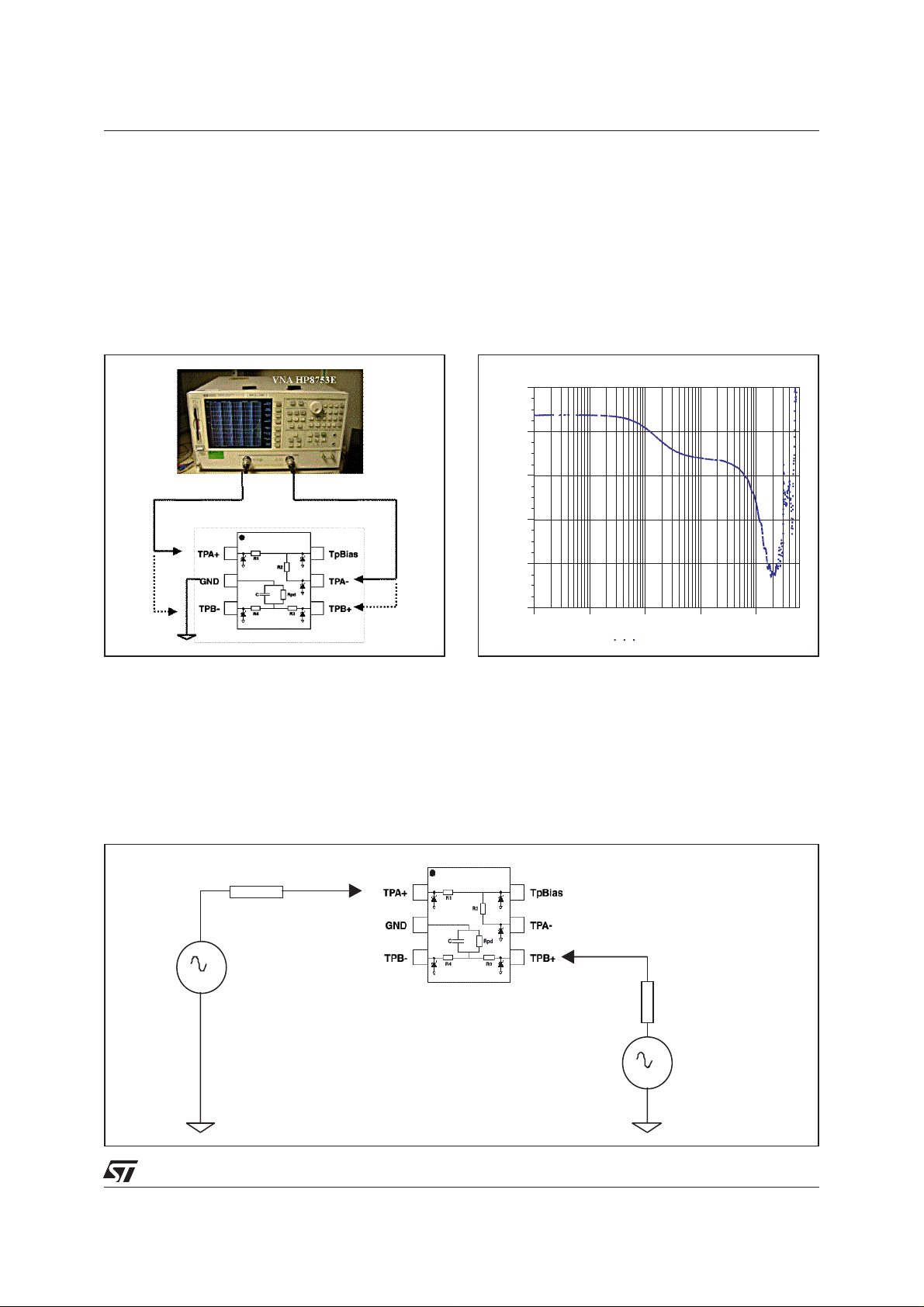
RF FILTER
Among allthe benefits the ST1394-01SC6 offers, there is one that allowsthedesigner to get a low-pass filter close to the IEEE1394 communication port especially dedicated to GSM bandwidth radiation.
The way the frequency response is measured is shown below:
Fig. 13: Frequency response measurement
set-up using HP8753E VNA (Vector Network
Fig. 14: Frequency response behavior on TPA
line.
Analyzer).
ST1394-SC6 : S21(dB)response
0.00
dB
-2.00
-4.00
-6.00
-8.00
-10.00
Thus frequency behavior is monitored and typical TPA or TPB response is given in
Aplac 7.70 User: ST Microelectronics Aug 29 2003
100.0k 1.0M 10.0M 100.0M 1.0G
Line 1
f/Hz
figure 14
.
Sinceone ST1394-01SC6 device managestwo data transmissionlines,some cross-talk phenomenoncan
be considered. This phenomenon could be explained by interferences from one line to the other due to internal undesirable coupling elements like parasitic capacitors or whatever.
Cross-talkanalysis consists in checkingthe impact of datatransmission of onelineon the otherduringdigital communication. The test set-up schematic given beneath tells more about it:
Fig. 15: Cross-talk set-up.
Rg
VNA
Port 1
Rg
VNA
Port 2
7/9
Page 8

Obsolete Product(s) - Obsolete Product(s) Obsolete Product(s) - Obsolete Product(s)
AN1783 - APPLICATION NOTE
Thiscross-talk measurement figureshowsthe parasitic disturbance is about -40dB for a 400Mb/s
signal from one line to the other.
As long as frequency measurement is considered,
caution must be taken in the way the measurements are performed. And particularly regarding
the PCB in order to minimize insertion losses and
reflectionphenomena mainly due tothe test board.
It should have the following features:
short tracks, 50Ω impedance adapted
n
coplanar structure, meaning ground plate lo-
n
cated at the back and top sides of the test PCB
ground vias on the entire pcb surface and all
n
along the access tracks (that connect the device
under test to the VNA equipment)
SMA connector located at the edge of the test
n
PCB.
Atest board exampleis shown inthenext
figure17
Fig. 17: RF test board picture (note the unused
lines are 50Ω loaded).
Fig. 16: Cross-talk response between one line
and the other with ST1394-01SC6 device versus
frequency.
ST1394_PM312 : S21(dB)response
0.00
-10.00
-20.00
-30.00
-40.00
-50.00
-60.00
-70.00
-80.00
-90.00
-100.00
:
Aplac 7.62 User: ST Microelectronics Jun 20 2003
dB
100.0k 1.0M 10.0M 100.0M 1.0G
Xtalk 1
f/Hz
Fig. 18: Calibration board for ST1394-01SC6
frequency response board analysis.
1cm
This is not all, by the way the VNA: itneeds tobe calibrated before the measurements are performed. This
imposes the use of a special calibration board that will previously set-up the analyzer and provides it the
test PCB characteristics. Those latter would be subtracted to the final measurements.
Typical calibration board developed for the ST1394-01SC6 frequency response board measurement is
given in
Once "Full two port" calibration is performed on VNA equipment, the ST1394-01SC6 frequency response
figure 18
analysis can be done.
.
8/9
Page 9

Obsolete Product(s) - Obsolete Product(s) Obsolete Product(s) - Obsolete Product(s)
AN1783 - APPLICATION NOTE
CONCLUSION
Fire-Wire communication port systems require ESD protection due to the possibility of external device
plugging, line termination due to fast data signal transmission in imperfect cable elements, GSM parasitic
frequency cut-off because this transmission connection can be used in mobiles environment.
As shown and described in this article, the ST1394-01SC6 device has been especially developed for
IEEE1394 communication port in order to fulfill:
ESD IEC61000-4-2 protection thanks to internal protection diodes
n
Line adaptation with integrated RC components
n
GSM bandwidth frequency cut-off
n
Easy implementation feature due to small SOT23-6L package
n
Informationfurnished is believed to beaccurateand reliable. However, STMicroelectronics assumes noresponsibility for the consequences of
useof such information nor forany infringement of patents orother rights of third partieswhich may result from itsuse.No license is granted by
implication or otherwise under any patent or patent rights of STMicroelectronics. Specifications mentioned in this publication are subject to
change without notice.This publication supersedes and replaces all information previously supplied. STMicroelectronics products are not authorized for use as critical components in life support devices or systems without express written approval of STMicroelectronics.
The ST logo is a registered trademark of STMicroelectronics.
All other names are the property of their respective owners.
© 2003 STMicroelectronics - All rights reserved.
Australia - Belgium - Brazil - Canada - China - Czech Republic - Finland - France - Germany -
Hong Kong - India - Israel - Italy - Japan - Malaysia - Malta - Morocco - Singapore - Spain -
STMicroelectronics GROUP OF COMPANIES
Sweden - Switzerland - United Kingdom - United States
www.st.com
9/9
 Loading...