

Page 1

AN1782
APPLICATION NOTE
STR71X I2C
COMMUNICATION WITH M24CXX EEPROM
INTRODUCTION
This application note gives an example of how to use the STR71x I2C peripheral to communicate with an I2C Protocol-Compatible Electrically Erasable Programmable Read Only Memory (EEPROM). The example uses the M24C08 EEPROM from STMicroelectronics.
The implemented software manages read and write operations between the STR71x I2C
interface and the M24C08.
1 STR71X I2C PERIPHERAL
The STR71x I2C peripheral provides both multi master and slave functions, and controls all
I2C bus-specific sequencing, protocol, arbitration and timing. It also provides the transfer
problem detection feature. The speed of the I2C interface may be selected between standard
(0-100KHz) and fast I2C (100-400KHz).
The STR71x provides two I2C interfaces I2C0 and I2C1.
Only the master characteristics of the STR71x I2C are needed to manage the communication
sequencing with EEPROM, which acts as a slave.
In this application, only the single master mode is used without error management.
To implement the I2C protocol, only 2 bidirectional lines are required, SCL (Serial Clock Line),
which carries the synchronization clock and SDA (Serial Data Line), which carries the bit to be
transmitted. This line is driven by the device that sends the data.
The corresponding port pins have to be configured as alternate function open drain.
Please refer to the STR71x reference manual for more details.
2 M24CXX EEPROM
The M24Cxx families of EEPROM are compatible with the I2C protocol. This EEPROM family
includes a range of different devices. Table 1 displays the size, the number of devices that can
be connected to the I2C bus and the number of blocks in each device.
Table 1. M24Cxx EEPROMs family characteristics
Device Size (Kbit) Devices per Bus Number of Blocks
M24C01 1 8 1
Rev. 2.0
AN1782/0905 1/7
1
Page 2
I2C COMMUNICATION BETWEEN STR71X AND M24CXX EEPROM
Device Size (Kbit) Devices per Bus Number of Blocks
M24C02 2 8 1
M24C04 4 4 2
M24C08 8 2 4
M24C016 16 1 8
3 STR71X/M24C08 COMMUNICATION APPLICATION
3.1 HARDWARE CONFIGURATION
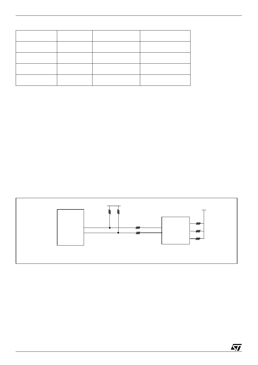
Two M24C08 memory chips can be addressed by a microcontroller on the same two wire bus
by configuring the M24C08 input E2. In this application the M24C08 E0, E1 and E2 inputs are
tied to V3.3 via 10K resistor. The M24C08 is divided into four blocks defined by the two LSB
bits of the memory address defined on the following:
■ M24C08_Block0 ==> ADDRESS 0xA8
■ M24C08_Block1 ==> ADDRESS 0xAA
■ M24C08_Block2 ==> ADDRESS 0xAC
■ M24C08_Block3 ==> ADDRESS 0xAE
Figure 1. STR71x/M24C08 configuration
STR71x
SDA
SCL
V3.3
4K7
4K7
100
100
SDA
SCL
M24C08
E2
E1
E0
V3.3
10K
10K
10K
3.2 SOFTWARE IMPLEMENTATION
In this application note the software modules are developed in C language, with RVDK envi-
ronment.
The software implemented to manage read and write operations between the STR71x I2C
interface and the M24C08 is divided in three parts:
– Write: first, the program writes the contents of a predefined buffer to the memory starting
from address 0x00 of Block3,
2/7
2
Page 3
I2C COMMUNICATION BETWEEN STR71X AND M24CXX EEPROM
– Wait: then, it waits until the write operation is finished,
– Read: finally it reads the data already written.
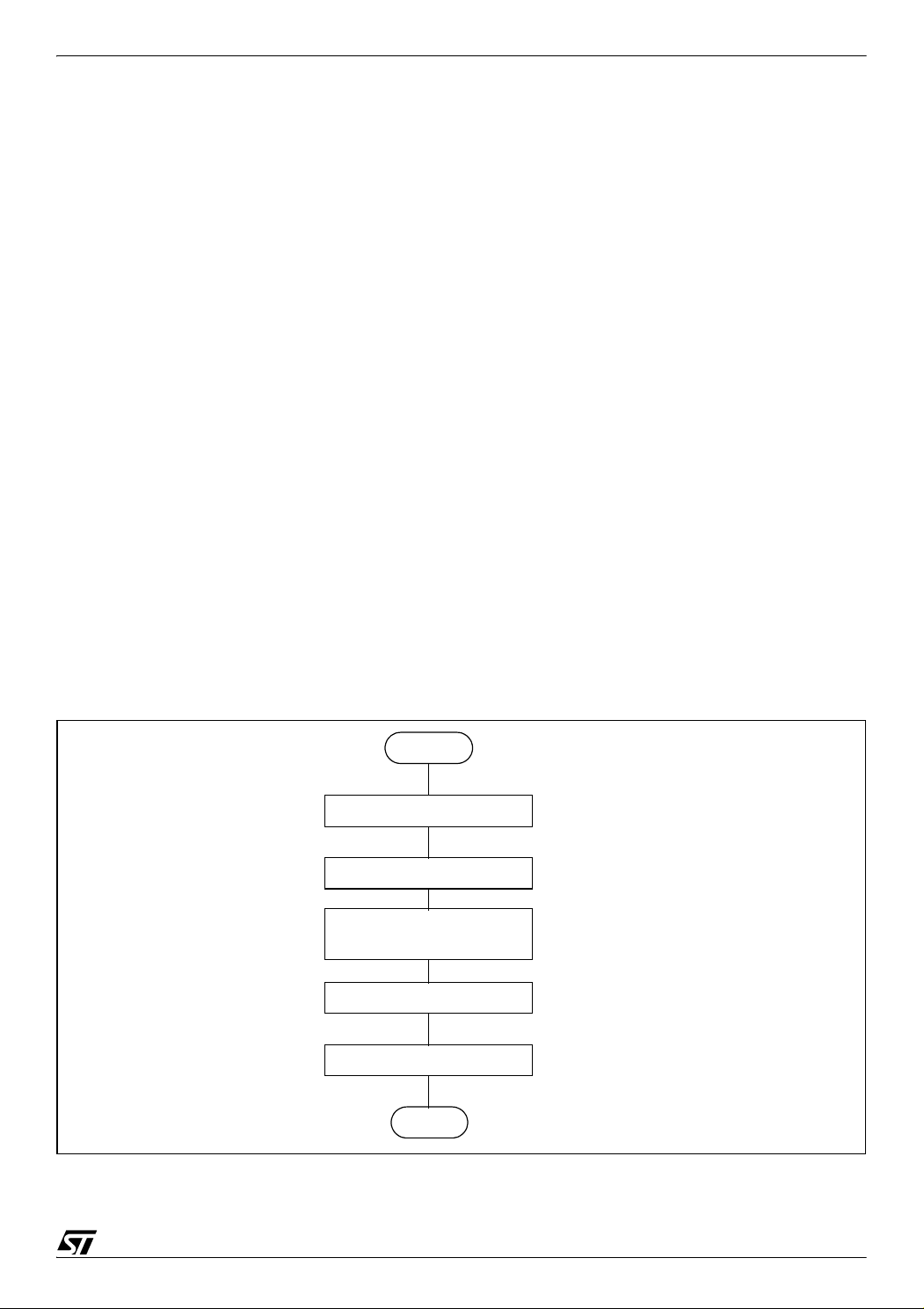
3.2.1 Write Operation
Before starting the communication, the I2C bus must be in the free state (SCL and SDA must
be HIGH). The write sequence is started by getting control of the bus. This action, which puts
the bus in busy state, is performed by setting the START bit in the Control Register (CR) in
order to generate a START Condition. Then the slave address is written in the Data Register
(DR) with the R/Wbit=0. This causes the address to be sent to the slave. The address transmission check is done by looping on the ENDAD flag in Status Register2 (SR2). This flag is
cleared by writing 0x20 in the Control Register (CR).
Then the master starts sending the data byte by writing it in the Data Register (DR). To
transmit a new data byte, the address or the data byte previously transmitted has to be completed correctly. The previous transmission check is done by looping on the BTF flag in Status
Register 1 (SR1). This flag is cleared by writing the next byte to be sent in the Data Register.
The first byte to be sent is the start address of the destination of the data.
A maximum of 16 bytes can be written to the M24C08 in a single write cycle.
The write sequence is ended by generating a STOP condition, by setting the STOP bit in the
Control Register (CR). This action releases the bus.
The following flowchart shows the different steps of the write cycle.
Figure 2. Write Operation Flowchart
Begin
Generate START Condition
Send Slave Address((R/W)bit=0)
Send the EEPROM’s internal
address to write to
Send String
Generate STOP Condition
End
3/7
Page 4

I2C COMMUNICATION BETWEEN STR71X AND M24CXX EEPROM
Example:
This example shows a write of data values 0x05 and 0xE0 to address 0x00 and 0x01 of
M24C08 Block3 respectively
START 0xAE 0 00 0 0x05 0 0xE0 0 STOP
Slave Address(R/W)=0 ACK Byte Address ACK DATA1 ACK DATA2 ACK
.
3.2.2 Wait for Write Operation
Before starting any new operation with the EEPROM, we wait until the write operation is finished. The EEPROM will send the ACK bit if busy with the write operation, so the processor
has to send the EEPROM address continuously until the EEPROM sends the ACK bit.
3.2.3 Read Operation
To initiate the communication, the STR71x I2C has to generate a START condition and then
send the M24C08 Address (with R/W bit cleared). After checking the correct status of the previous transmission, the Master writes, in the Data Register (DR), the address of the first byte
we want to read from the M24C08. The previous byte transmission check is done by looping
on the BTF flag in the Status Register 1 (SR1).
Then the STR71x I2C has to regenerate the START condition and then write the slave address in the Data Register (DR). This address must be the same as the address sent after the
first START condition except that the least significant bit (R/W) must be set. Then a previous
byte transmission check is done by looping on the ENDAD flag in Status Register 2 (SR2).
After this, the STR71x I2C becomes a receiver for all bytes sent from the M24C08. To receive
a new data byte, the previous byte reception has to be completed correctly. The byte reception
check is done by looping on the BTF flag in Status Register 1 (SR1). This flag is cleared by
reading the Data Register (DR).
To close the communication, before reading the last byte from the DR register, set the STOP
bit to generate the Stop condition. The interface goes automatically back to slave mode (M/SL
bit cleared). In order to generate the non-acknowledge pulse after the last received data byte,
the ACK bit must be cleared just before reading the second last data byte.
4/7
Page 5

I2C COMMUNICATION BETWEEN STR71X AND M24CXX EEPROM
Figure 3. Read Operation Flowchart
Send Slave Address((R/W)bit=0)
Begin
Generate START Condition
Send the EEPROM’s address to
Send Slave Address((R/W)bit=1)
Wait until the byte is received
No
No
Enable STOP condition generation
read from
Re-Generate START
2nd last byte to
receive
Ye s
Disable ACK
Last byte to receive
Ye s
No
Receive next byte
End of reception
Ye s
End
5/7
Page 6

I2C COMMUNICATION BETWEEN STR71X AND M24CXX EEPROM
Example:
This example shows a read of two bytes from address 0x00 and 0x01 of M24C08 Block3.
START 0xAE 0 00 0 RESTART 0xAF DATA1
(Out)
Slave Address
(R/W)=0
ACK Byte Address ACK Slave Address
(R/W)=1
DATA1 ACK DATA1 NoACK STOP
0 DATA2
(Out)
1 STOP
6/7
Page 7

I2C COMMUNICATION BETWEEN STR71X AND M24CXX EEPROM
“THE PRESENT NOTE WHICH IS FOR GUIDANCE ONLY AIMS AT PROVIDING CUSTOMERS WITH INFORMATION
REGARDING THEIR PRODUCTS IN ORDER FOR THEM TO SAVE TIME. AS A RESULT, STMICROELECTRONICS
SHALL NOT BE HELD LIABLE FOR ANY DIRECT, INDIRECT OR CONSEQUENTIAL DAMAGES WITH RESPECT TO
ANY CLAIMS ARISING FROM THE CONTENT OF SUCH A NOTE AND/OR THE USE MADE BY CUSTOMERS OF
THE INFORMATION CONTAINED HEREIN IN CONNECTION WITH THEIR PRODUCTS.”
Information furnished is believed to be accurate and reliable. However, STMicroelectronics assumes no responsibility for the consequences
of use of such information nor for any infringement of patents or other rights of third parties which may result from its use. No license is granted
by implication or otherwise under any patent or patent rights of STMicroelectronics. Specifications mentioned in this publication are subject
to change without notice. This publication supersedes and replaces all information previously supplied. STMicroelectronics products are not
authorized for use as critical components in life support devices or systems without express written approval of STMicroelectronics.
The ST logo is a registered trademark of STMicroelectronics.
All other names are the property of their respective owners
© 2005 STMicroelectronics - All rights reserved
STMicroelectronics group of companies
Australia – Belgium - Brazil - Canada - China – Czech Republic - Finland - France - Germany - Hong Kong - India - Israel - Italy - Japan -
Malaysia - Malta - Morocco - Singapore - Spain - Sweden - Switzerland - United Kingdom - United States of America
www.st.com
7/7
 Loading...