

Page 1

Application note
TS4990 low voltage audio power amplifier
Evaluation board user guidelines
TS4990 features
■ TS4990 low voltage audio power amplifier with active low standby mode
■ Operating from V
■ 1.2W output power @ V
■ Ultra low power consumption in standby mode (10nA)
■ 62dB PSRR @ 217Hz in grounded mode (Av=2V/V)
■ Near zero pop & click
■ Ultra low distortion (0.1%)
■ Module gain set at 2V/V
■ Thermal and short circuit protection
Description
=2.2V to 5.5V
CC
CC
=5V, THD=1%, F=1kHz, with 8Ω load
AN1766
The DEMO TS4990 is an evaluation board designed for the TS4990 low power audio
amplifier. The micropackage DFN8 (dual flat non leaded 8 pins) allows space saving and
good thermal dissipation.
The BTL gain is set at 2V/V and can be ad apted if necessary with a modificati on of R1 or R2
values.
On the board, R3 and C3 component locations are empty to allow you to modify the input
configuration from single ended to differential. For differential mode, R4 must be modified.
The C1 component location is also empty so that you can add a low pass filter if required.
More information about component calculations is available in the TS4990 datasheet.
November 2006 Rev 3 1/5
www.st.com
Page 2
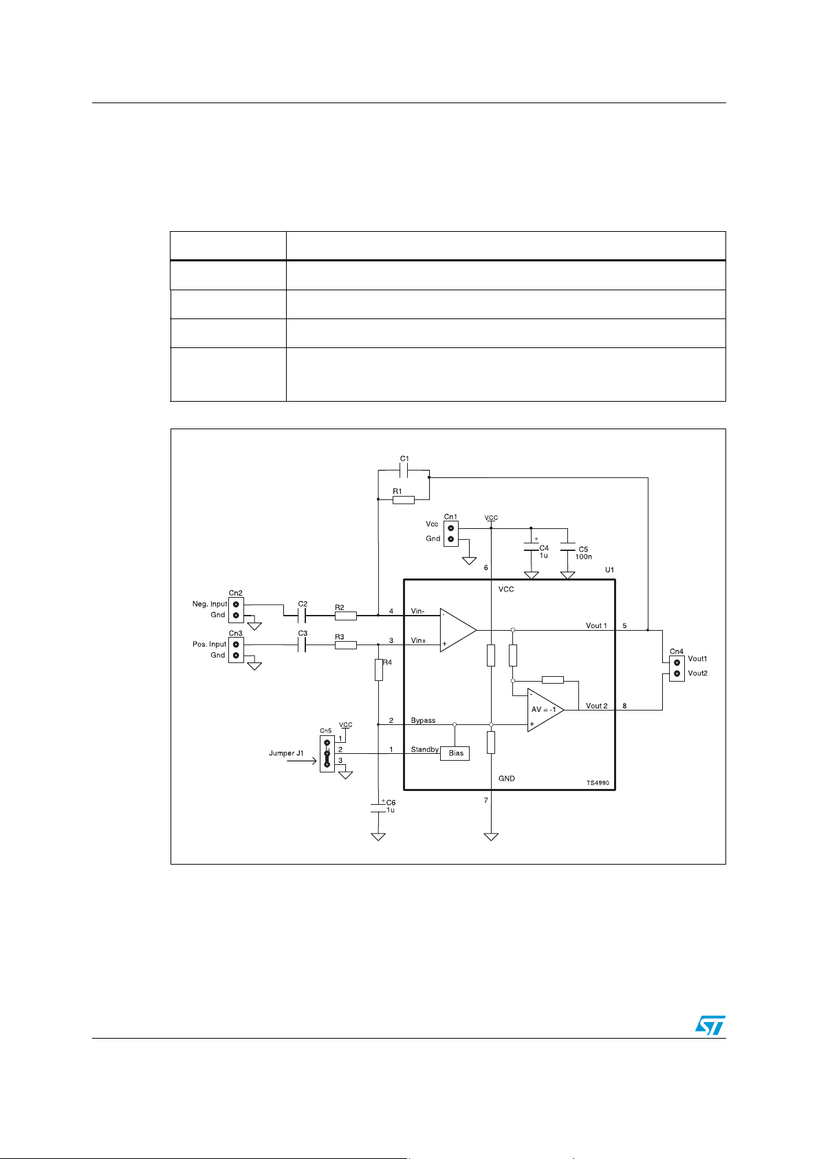
Connector configuration AN1766
Connector configuration
Caution: When you apply power supply through Cn1, DO NOT invert the polarity because it would
destroy the amplifier U1.
Connector Description
Cn1 Pow er connector (V
and GND). Power supply voltage from 2.2V to 5.5V.
CC
Cn2 and Cn3 Input signal connector (GND and active input signal).
Cn4 Output signal connector (V
Standby control connector (V
Cn5
and standby puts U1 in operation mode. A short-circuit between GND and
and V
out1
, standby, GND). A short-circuit between VCC
CC
out2
).
Standby puts U1 in standby mode.
Figure 1. Schematic diagram
2/5
Page 3

AN1766 Component list for the DEMO TS4990/DFN
Component list for the DEMO TS4990/DFN
Designation Quantity Description
C1 0 Unconnected, ceramic capacitors, 0603
C2 1 100nF/16V, ceramic capacitors, 0603
C3 0 Unconnected, ceramic capacitors, 0603
C4 1 1μF/50V, electrolytic capacitor
C5 1 100nF/16V, ceramic capacitors, 0603
C6 1 1μF/50V, electrolytic capacitor
Cn1 1 2 pins header 2.54mm pitch
Cn2 1 2 pins header 2.54mm pitch
Cn3 1 2 pins header 2.54mm pitch
Cn4 1 2 pins header 2.54mm pitch
Cn5 1 3 pins header 2.54mm pitch
J1 1 Jumper, 2.54mm pitch
R1 1 22k, 1/16W 1% resistor, 0603
R2 1 22k, 1/16W 1% resistor, 0603
R3 0 Unconnected, 1/16W 1% resistor, 0603
R4 1 0R, 1/16W 1% resistor, 0603
U1 1 TS4990IQ (DFN8 package)
3/5
Page 4

Evaluation board layout AN1766
Evaluation board layout
The following schematics show the different layers and the top view of the evaluat ion board.
Figure 2. PCB top layer view Figure 3. PCB bottom layer view
Figure 4. Top view of demo board
4/5
Page 5

AN1766
Please Read Carefully:
Information in this document is provided solely in connection with ST products. STMicroelectronics NV and its subsidiaries (“ST”) reserve the
right to make changes, corrections, modifications or improvements, to this document, and the products and services described herein at any
time, without notice.
All ST products are sold pursuant to ST’s terms and conditions of sale.
Purchasers are solely res ponsibl e fo r the c hoic e, se lecti on an d use o f the S T prod ucts and s ervi ces d escr ibed he rein , and ST as sumes no
liability whatsoever relati ng to the choice, selection or use o f the ST products and services described herein.
No license, express or implied, by estoppel or otherwise, to any intellectual property rights is granted under this document. If any part of this
document refers to any third pa rty p ro duc ts or se rv ices it sh all n ot be deem ed a lice ns e gr ant by ST fo r t he use of su ch thi r d party products
or services, or any intellectua l property c ontained the rein or consi dered as a warr anty coverin g the use in any manner whats oever of suc h
third party products or servi ces or any intellectual property contained therein.
UNLESS OTHERWISE SET FORTH IN ST’S TERMS AND CONDITIONS OF SALE ST DISCLAIMS ANY EXPRESS OR IMPLIED
WARRANTY WITH RESPECT TO THE USE AND/OR SALE OF ST PRODUCTS INCLUDING WITHOUT LIMITATION IMPLIED
WARRANTIES OF MERCHANTABILITY, FITNESS FOR A PARTICUL AR PURPOS E (AND THEIR EQUIVALE NTS UNDER THE LAWS
OF ANY JURISDICTION), OR INFRINGEMENT OF ANY PATENT, COPYRIGHT OR OTHER INTELLECTUAL PROPERTY RIGHT.
UNLESS EXPRESSLY APPROVED IN WRITING BY AN AUTHORIZED ST REPRESENTATIVE, ST PRODUCTS ARE NOT
RECOMMENDED, AUTHORIZED OR WARRANTED FOR USE IN MILITARY, AIR CRAFT, SPACE, LIFE SAVING, OR LIFE SUSTAINING
APPLICATIONS, NOR IN PRODUCTS OR SYSTEMS WHERE FAILURE OR MALFUNCTION MAY RESULT IN PERSONAL INJ URY,
DEATH, OR SEVERE PROPERTY OR ENVIRONMENTAL DAMAGE. ST PRODUCTS WHICH ARE NOT SPECIFIED AS "AUTOMOTIVE
GRADE" MAY ONLY BE USED IN AUTOMOTIVE APPLICATIONS AT USER’S OWN RISK.
Resale of ST products with provisions different from the statements and/or technical features set forth in this document shall immediately void
any warranty granted by ST fo r the ST pro duct or serv ice describe d herein and shall not cr eate or exten d in any manne r whatsoever , any
liability of ST.
ST and the ST logo are trademarks or registered trademarks of ST in various countries.
Information in this document su persedes and replaces all information previously supplied.
The ST logo is a registered trademark of STMicroelectronics. All other names are the property of their respective owners.
© 2006 STMicroelectronics - All rights reserved
STMicroelectronics group of compan ie s
Australia - Belgium - Brazil - Canada - China - Czech Republic - Finland - France - Germany - Hong Kong - India - Israel - Italy - Japan -
Malaysia - Malta - Morocco - Singapore - Spain - Sweden - Switzerland - United Kingdom - United States of America
www.st.com
5/5
 Loading...