

AN1762
APPLICATION NOTE
L6205, L6206, L6207 DUAL FULL BRIDGE DRIVERS
by Vincenzo Marano
Modern motion control applications need more flexibility that can be addressed only with specialized IC
products. The L6205, L6206, L6207 are dual full bridge drivers ICs specifically developed to drive a wide
range of motors. These ICs are one-chip cost effective solutions that include several unique circuit design
features. These features allow the devices to be used in many applications including DC and stepper motor
driving. The principal aim of this development project was to produce easy to use, ful ly protected pow er ICs.
In addition several k ey functi ons s uch as pr otection circuit and PW M current c ontrol drastic ally r educe external components count to meet requirements for many different applications.
1 INTRODUCTION
The L6205, L6206, L6207 are highly integrated, mixed-signal power ICs that allow the user to easily design a
control system for two-phase bipolar stepper motors, multiple DC motors and a wide range of inductive loads.
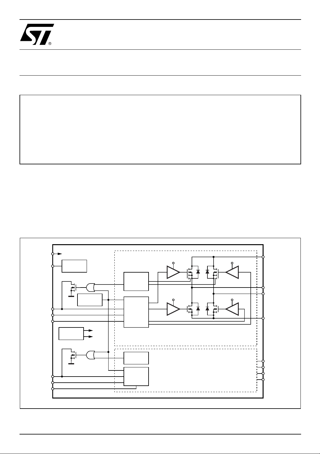
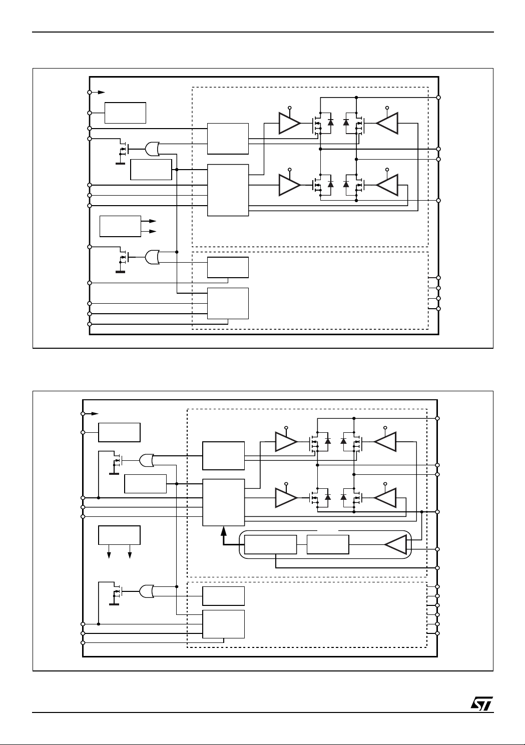
Figure 1 to Figure 3 show the L6205, L6206, L6207 block di agrams. Each IC integrates eight Power DMOS pl us
other added features for safe operation and flexibility. The L6207 also features a constant t
control technique (
Synchronous mode
) for each of the two full bridges.
PWM current
OFF
Figure 1. L6205 block diagram.
VBOOT
VCP
EN
IN1
IN2
EN
IN1
IN2
A
A
A
B
B
B
V
BOOT
CHARGE
PUMP
VOLTAGE
REGULA TOR
OCD
THERMAL
PROTECTION
10V
5V
OCD
A
B
OVER
CURRENT
DETECTION
GA TE
LOGIC
OVER
CURRENT
DETECTION
GA TE
LOGIC
V
BOOT
10V 10V
V
BOOT
BRIDGE A
BRIDGE B
D99IN1091A
VS
A
OUT1
OUT2
SENSE
V
S
B
OUT1
OUT2
SENSE
A
A
A
B
B
B
December 2003
1/53
AN1762 APPLICATION NOTE
Figure 2. L6206 block diagram.
VBOOT
VCP
PROGCL
OCD
EN
IN1
IN2
OCD
A
A
A
A
A
B
V
BOOT
CHARGE
PUMP
VOLTAGE
REGULA TOR
OCD
THERMAL
PROTECTION
10V
5V
OCD
PROGCL
B
EN
B
IN1
B
IN2
B
Figure 3. L6207 block diagram.
VS
V
BOOT
OVER
A
CURRENT
DETECTION
V
BOOT
10V 10V
GA TE
LOGIC
A
OUT1
OUT2
SENSE
A
A
A
BRIDGE A
OVER
B
CURRENT
DETECTION
GA TE
LOGIC
V
S
B
OUT1
OUT2
SENSE
B
B
B
BRIDGE B
D99IN1088A
VBOOT
VCP
EN
IN1
IN2
EN
IN1
IN2
A
A
A
B
B
B
V
BOOT
CHARGE
PUMP
PROTECTION
VOLTAGE
REGULATOR
5V10V
THERMAL
OCD
OCD
VS
V
BOOT
A
OVER
CURRENT
DETECTION
V
BOOT
10V 10V
GATE
LOGIC
A
OUT1
OUT2
SENSE
A
A
A
PWM
BRIDGE A
+
-
VREF
RC
A
V
S
B
OUT1
OUT2
SENSE
VREF
RC
B
A
B
B
B
B
ONE SHOT
MONOSTABLE
OVER
CURRENT
B
DETECTION
GATE
LOGIC
MASKING
TIME
SENSE
COMPARATOR
BRIDGE B
D99IN1085A
2/53

AN1762 APPLICATION NOTE
Table of Contents
1 INTRODUCTION................................................................................................................................ 1
2 MAIN DIFFERENCES BETWEEN L6205, L6206 , L6207 ..................................................................4
3 DESIGNING AN AP PLICATI ON WITH L6205, L6206, L6207 ...........................................................4
3.1 Current Ratings........................................................................................................................4
3.2 Voltage Rating s and Operating Range ....................................................................................4
3.3 Choosing th e Bulk Capacitor....................................................................................................6
3.4 Layout Considerations.............................................................................................................7
3.5 Sensing Resisto r s.............................. ......................................................... ..................... ....... .9
3.6 Charge pump external components.......................................................................................10
3.7 Sharing the Charge Pump Circuitry .......................................................................................11
3.8 Reference Voltage for PWM Current Control (L6207 ONLY).................................................12
3.9 Input Logic pins......................................................................................................................13
3.10 EN pins...................................................................................................................................13
3.11 Program mab le off-time Monost able (L6207 ON LY)..............................................................14
3.11.1 Off-time Selection and minimum on-time (L6207 ONLY) ................................................16
3.11.2 Slow Decay Mode (L6207 ONLY) ...................................................................................17
3.12 Over Current Protection........................................................................................................18
3.13 Adjusting the Over Current Detection trip point (L6206 ONLY)............................................21
3.14 Paralleling two Full Bridges...................................................................................................23
3.14.1 Paralleling two Full Bridges to get a single Full Bridge ....................................................23
3.14.2Paralleling the four Half Bridges to get a single Half Bridge.............................................26
3.15 Power Managem ent..............................................................................................................27
3.15.1 Maximum output current vs. selectable devices..............................................................27
3.15.2 Power Dissipation Formulae for different sequences......................................................28
4 APPLICATION EXAMPLE (L6207)..................................................................................................32
4.1 Decay mode, sensing resistors and reference voltage..........................................................32
5 APPENDIX - EVALUATI ON BO ARD S...................................................................... .......................33
5.1 PractiSPIN............................................................................. .................................................33
5.2 EVAL6205N ...........................................................................................................................34
5.2.1 Important Not e s......... ................................... ......................................................... ....... ....35
5.3 EVAL6206N ...........................................................................................................................39
5.3.1 Important Not e s......... ................................... ......................................................... ....... ....40
5.4 EVAL6206PD.........................................................................................................................44
5.4.1 Important Not e s......... ................................... ......................................................... ....... ....45
5.5 EVAL6207N ...........................................................................................................................49
5.5.1 Important Not e s......... ................................... ......................................................... ....... ....50
6 REFERENCES....................................................................................... ..........................................53
3/53

AN1762 APPLICATION NOTE
2 MAIN DIFFERENCES BETWEEN L6205 , L6206, L6207
L6205, L6206 and L6207 are DMOS Dual Full Bridge ICs.
L6205 (see Figure 1) includes logic for CMOS/TTL interface, a charge pump that provide auxiliary voltage to
drive the high-side DMOS, non dissipative over current protection circuitry on the high-side DMOS, with fixed
trip point set at 5.6 A (see
Out for reliable start-up.
In addition, L6206 gives the possibility of adjusting the trip point of the over current protection for each of the
two full-bridges (through two external resistors), and its internal open-drain mosfets (see
tion
Section) are not internally connected to EN pins but to separate
tics and overcurrent management.
L6207 has Over Current protection function with fixed trip point set at 5.6 A and internal open-drain mosfets
connected to
bridges (see
EN
pins, as the L6205, but it also integrates two PWM current controller for each of the two full-
Programmable off-time Monostable
3 DESIGNING AN APPLICATION WITH L6205, L6206, L6207
3.1 Current Ratings
With MOSFET (DMOS) devices, unlike bipolar transistors, current under short circuit conditions is, at first approximation, limited by the R
L6207
Out
pins and the two VSA and VSB pins are rated for a maximum of 2.8A r.m.s. and 5.6A peak (typical
values), corresponding to a total (for the whole IC) 5.6A rms (11.2A peak). These values are meant to avoid
damaging metal structures, including the metallization on the die and bond wires. In practical applications,
though, maximum allowable current is less than these values, due to power dissipation limits (
Management
section
against short circuits between the outputs and between an output and ground (
sect ion
).
Over Current Protection
Section), over temperature protection, Under Voltage Lock-
Over Current Protec-
OCD
pins,
allowing eas ier external dia gnos-
section).
of the DMOS themselves and could reach very high values. L6205, L6206,
DS(ON)
see
Powe r
). The devices have a built-in Over Current Detection (OCD) that provides protection
see
Over Current Protection
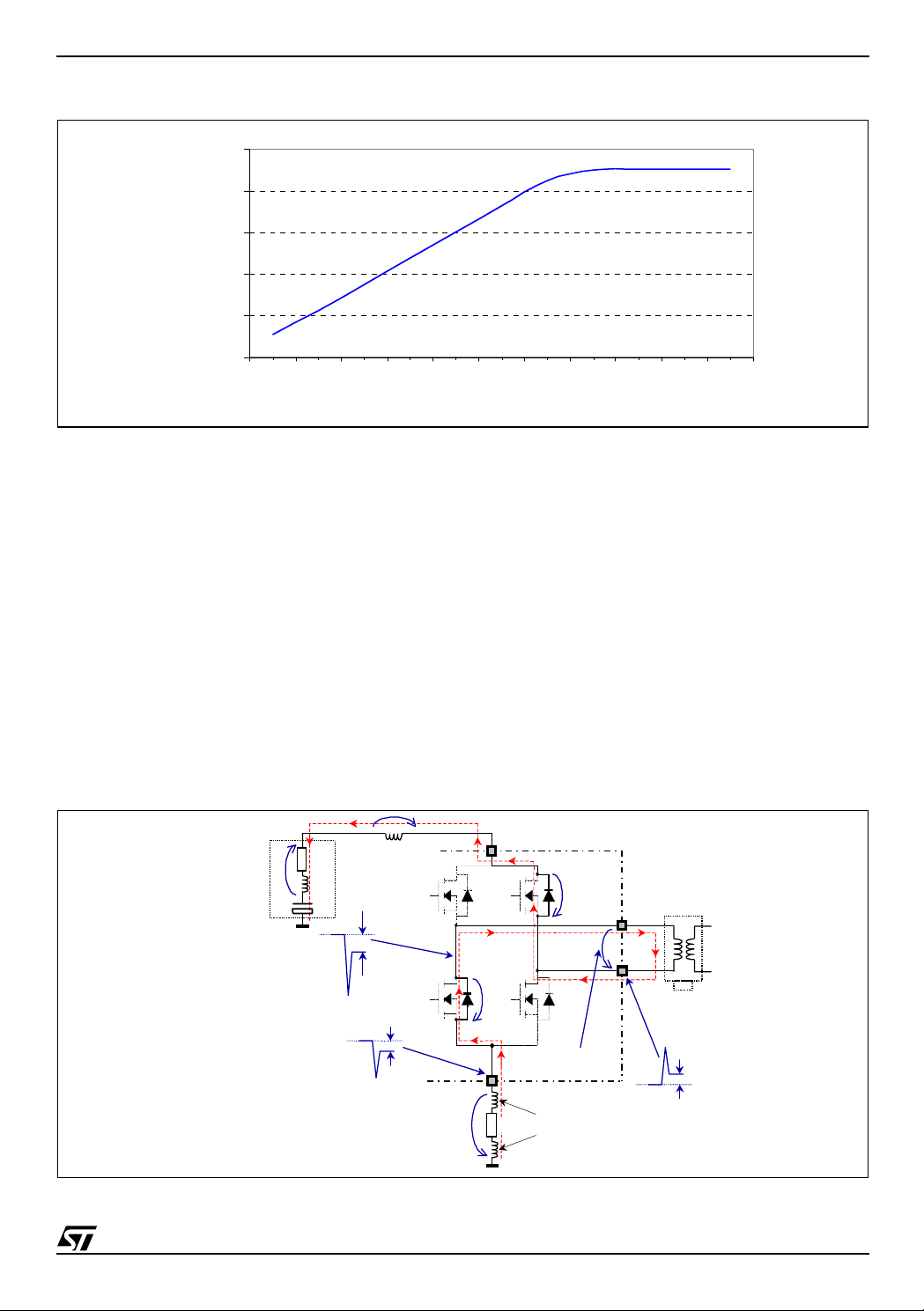
3.2 Voltage Ratings and Operating Range
The L6205, L6206, L6207 requires a si ngle supply voltage (VS), for the motor supply. Internal voltag e regulators
provide the 5V and 10V required for the internal circuitry. The operating range for V
working into undesirable low supply volt age an
when supply voltage falls below 6V; to resume normal oper ating condi tions, V
Under Vol tage Lock Out
(
UVLO
must then exceed 7V. The hys-
S
teresis is provided to avoid false intervention of the UVLO function during fast V
however, that DMOS's R
R
is adversely affected, and this is particularly true for the High Side DMOS that are driven from V
DS(ON)
is a function of the VS supply voltage. Actually, when VS is less than 10V,
DS(ON)
is 8 to 52V. To prevent
S
) circuit shuts down the device
ringings. It should be noted,
S
BOOT
supply. This supply is obtained through a charge pump from the internal 10V supply, which will tend to reduce
its output voltage when V
(V
4/53
- VS) versus the supply voltage (VS).
BOOT
goes below 10V. Figure 4 shows the supply voltage of the high side gate drivers
S
AN1762 APPLICATION NOTE
Figure 4. High side gate drivers supply voltage versus supply volta ge.
8
7.6
V
- V
BOOT
[V]
Note that VS must be connected to both VSA and VSB since the bootstrap voltage (at V
7.2
S
6.8
6.4
6
8 8.5 9 9.5 10 10.5
[V]
V
S
pin) is the same for
BOOT
the two H-bridges. The integrated DMOS have a rated Drain-Source breakdown voltage of 60V. However V
should be kept below 52V, since in normal working conditions the DMOS see a Vds voltage that will exceed V
supply. In particular, during a phase change ( when each output of the same H-bridge sw itches from VS to GND
or vice versa, for example to reverse the current in the load) at the beginning of the dead-time (when all the
DMOS are off) the
path from the pin to GND. This spike is followed by a stable negative voltage due to the drop on R
of the two
OUT
SENSE
pin sees a negative spike due to a not negligible parasitic inductance of the PCB
. One
SENSE
pins of the bridge sees a similar behavior, but with a slightly larger voltage due to the forward
recovery time of the integrated freewheeling di ode and the forward voltage drop ac ross it (see Figure 5). Typical
duration of this spike is 30ns . At the same time, the other
OUT
pin of the same bridge sees a vol tage above VS,
due to the PCB in ductance and v oltage drop across the h igh-side ( integrated) freewheeling diode, as the current
reverses direction and flows into the bulk capacitor. It turns out that the highest differential voltage can be observed between the two
OUT
pins of the same bridge, during the dead-time at a phase change, and this must
always be kept below 60V [3].
S
S
Figure 5. Currents and voltages during the
PCB Parasitic
Inductance
R
*I+V
SENSE
R
SENSE
Bulk Capacitor
Equivalent Circuit
ESR
ESL
dead time
F(Diode)
*I
SENSE
at a phase change.
V
S
OUT
OUT
Dangerous
High Differential Voltage
PCB Par a s i ti c
R
SENSE
Inductan ce
2
1
VS+V
F(Diode)
5/53
AN1762 APPLICATION NOTE
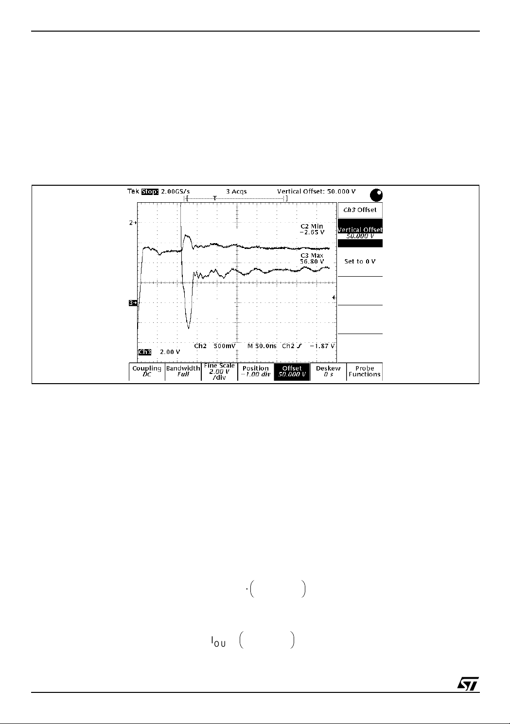
Figure 6 shows the voltage waveform s at the two OUT pins referring to a pos sible pr actical situ ation, with a peak
output current of 2.8A, V
ground spike amplitude is -2.65V for one output; the other
differential voltage reaches almost 60V, which is the a bsolute max imum rating for the DMOS. Keepi ng differential voltage between two Output pins belonging to the same Full Bridge within rated values is a must that can
be accomplished with proper selection of Bulk capacitor value and equivalent series resistance (ESR), according to current peaks and chopping style and adopting good layout practices to minimize PCB parasitic inductances (see below) [3].
= 52V, R
S
= 0.33Ω, TJ = 25°C (approximately) and a good PCB layout. Below
SENSE
OUT
pin is at about 57V . In these conditions, total
Figure 6. Vol ta ge a t th e tw o outputs duri ng the
Out 1
Out 2
dead time
at a phase change.
3.3 Choosing the Bulk Capacitor
Since the bulk capacitor, placed between VS and
AC current capability
must be greater than the r.m.s. value of the charge/discharge current. In the case of a
PWM current regulation, the current flows from the capacitor to the IC during the on-time (t
GND
pins, is charged and discharged during IC operation, its
) and from the IC
ON
(implementing a fast decay current recirculation technique) or from the power supply (implementing a slow decay current recirculation technique) to the capacitor during the off-time (t
). The r.m.s. value of the current
OFF
flowing into the bulk capacito r depends on peak output curr ent, outp ut current r ippl e, switchin g fr equency, dutycycle and chopping style. It also depends on power supply characteristics. A power supply with poor high frequency performances (or long, inductive connections to the IC) will cause the bulk capacitor to be recharged
slowly: the higher the current control switching frequency, the higher the current ripple in the capacitor; r.m.s.
current in the capacitor, however, does not exceed the r.m.s. output current. Bulk capacitor value (
ESR
determine the amount of voltage ripple on the capacitor itself and on the IC. In slow decay, neglecting the
dead-time
power supply, the voltage at the end of the
and output current ripple, and assumin g that during the
on-time
is:
on-time
the capacitor is not recharged by the
C
) and the
so the supply voltage ripple is:
6/53
VSI
– ESR
OUT
I
⋅
OUT
t
t
---------+
ON
C
-------- -+
ON
C
,
,
⋅
ESR

AN1762 APPLICATION NOTE
where I
is the output current. With fast decay, i nstead, recirculating curr ent recharges the capacitor , causing
OUT
the supply voltage to exceed the nominal voltage. This can be very dangerous if the nominal supply voltage is
close to the maximum recommended supply voltage (52V). In fast decay the supply voltage ripple is about:
t
+
I
OUT
2 ESR⋅
⋅
ONtOFF
--------------------------- -+
C
,
always assuming that the power supply does not recharge the capacitor, and neglecting the output current ripple
and the dead-time. Usually (if C > 100 µF) the capacitance role is much less than the ESR, then supply v oltage
ripple can be estimated as:
I
· ESR in slow decay
OUT
2 · I
For Example, if a maximum ri pple of 500mV is all owed and I
0.5V
ESR
------------
< 250mΩ=
1
---
2
Actually, current sunk by V
ESR
and VSB pins of the device is subject to higher peaks due to reverse recovery
SA
· ESR in fast decay
OUT
2A
0.5V
------------
⋅< 125mΩ=
2A
= 2A, the capacitor ESR should be lower than:
OUT
in slow decay, and
in fast decay.
charge of internal freewheeling diodes. Duration of these peaks is, tough, very short, and can be filtered using
a small value (100÷200 nF), good quality ceramic capacitor, connected as close as possible to the V
and GND pins of the IC. Bulk capacitor will be chosen with
maximum operating voltage
25% greater than the
SA
, V
SB
maximum supply voltage, considering also power supply tolerances. For example, with a 48V nominal power
supply, with 5% tol erance, maximum voltage is 50.4V, then operati ng voltage for the capacitor should be at least
63V.
3.4 Layout Considerations
Working with devices that combine high power switches and control logic in the same IC, careful attention has
to be paid to the PCB lay out. In extreme cases, Power DMOS commutation can i nduce nois es that could c ause
improper operation in the logic section of the device. Noise can be radiated by high dv/dt nodes or high di/dt
paths, or conducted through G ND or Supply connectio ns. Logic connec tions, es pecial ly hi gh-i mpedance nodes
(actually all logic inputs, see furt her), must be kept far from switching nodes and paths. With the L6205, L6206,
L6207, in particular, external components for the charge pump circuitry should be connected together through
short paths, since these components are subject to voltage and current switching at relatively high frequency
(600kHz). Primary mean in minimizing conducted noise is working on a good GND layout (see Figure 7).
7/53
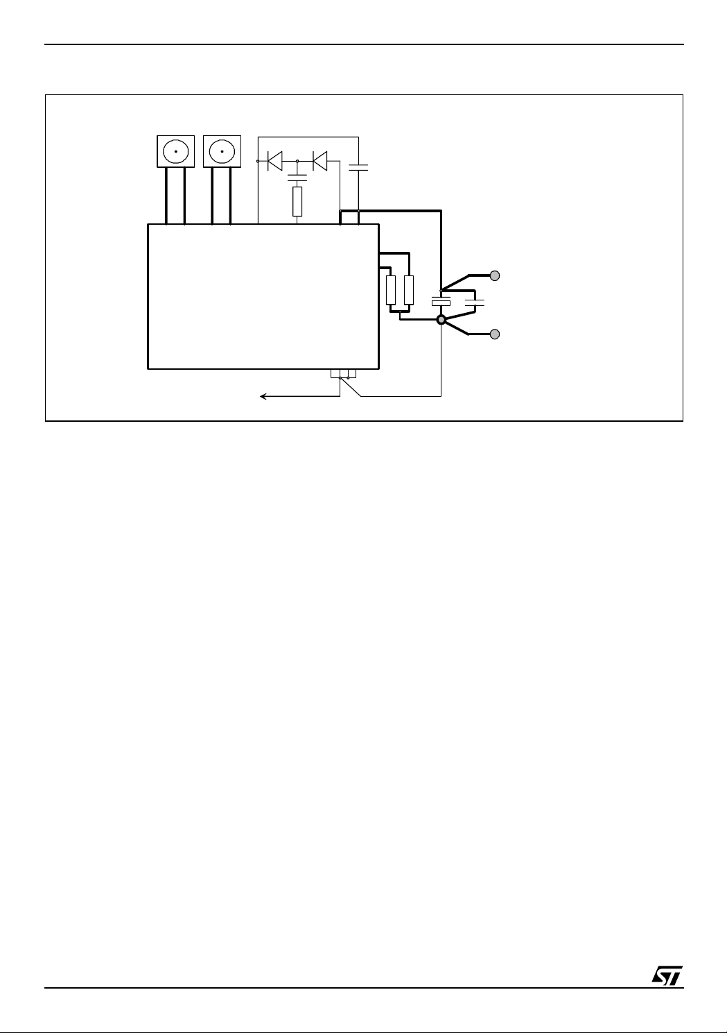
AN1762 APPLICATION NOTE
Figure 7. Typ ic a l App li ca ti on and Layout suggest io ns.
Motors or
other loads
D1
D2
C1
R1
C4
OUT
OUT
OUT
1A
2A
V
OUT
1B
2B
BOOT
CP
L6205, L6206, L6207
V
SA VSB
SENSE
A
SENSE
B
RS1 RS2
C2
+
C3
VS = 8 ÷ 52 V
-
GND
GND
Logic
GND
High current GND tracks (i.e. the tracks connected to the sensing resistors) must be connected directly to the
negative terminal of the bulk capacitor. A good quality, high-frequency bypass capacitor is also required (typically a 100nF÷200nF ceramic would suffice), since electrolytic capacitors show a poor high frequency performance. Both bulk electrolytic and high frequency bypass capacitors have to be connected with short tracks to
V
, VSB and GND. On the L6205, L6206, L6207 GND pins are the
SA
flows through them. Logic GND and Power GND should be connected together in a
pacitor, to keep noise in the Power GND from affecting Logic GND. Specific care should be paid layouting the
path from the
SENSE
pins through the sensing resistors to the negative terminal of the bulk capacitor (Power
Ground). These tracks must be as short as possible in order to minimize parasitic inductances that can cause
dangerous voltage spikes on
for the same reason the capacitors on V
SENSE
and
OUT
, VSB and GND should be very close to the GND and supply pins.
SA
Refer to the Sensing Resistors section for information on selecting the sense resistors. Traces that connect to
, VSB, SENSEA, SENSEB, and the four
V
SA
OUT
are flowing through these traces, and layer changes should be avoided. Should a layer change prove necessary, multiple and large via holes have to be used. A wide GND copper area can be used to improve power
dissipation for the device.
Figure 8 shows two typical situations that must be avoided. An important consideration about the location of the
bulk capacitors is the abi lity to abs orb the inductiv e ener gy from the load, without all owing the s upply v oltage to
exceed the maximum rating. The diode shown in Figure 8 prevents the recirculation current from reaching the
capacitors and will res ult in a high voltage on the IC pins th at can destroy the device. H aving a switch or a power
connection that can dis connect the c apacitors from the IC, w hile there is stil l c ur rent in the motor, will a lso result
in a high voltage transient since there is no capacitance to absorb the recirculation current.
GND
GND
pins (see the
Logic
GND, since only the quies cent current
single point
Voltage Ratings and Operating Range
, the bulk ca-
section);
pins must be designed with adequate width, since high currents
8/53
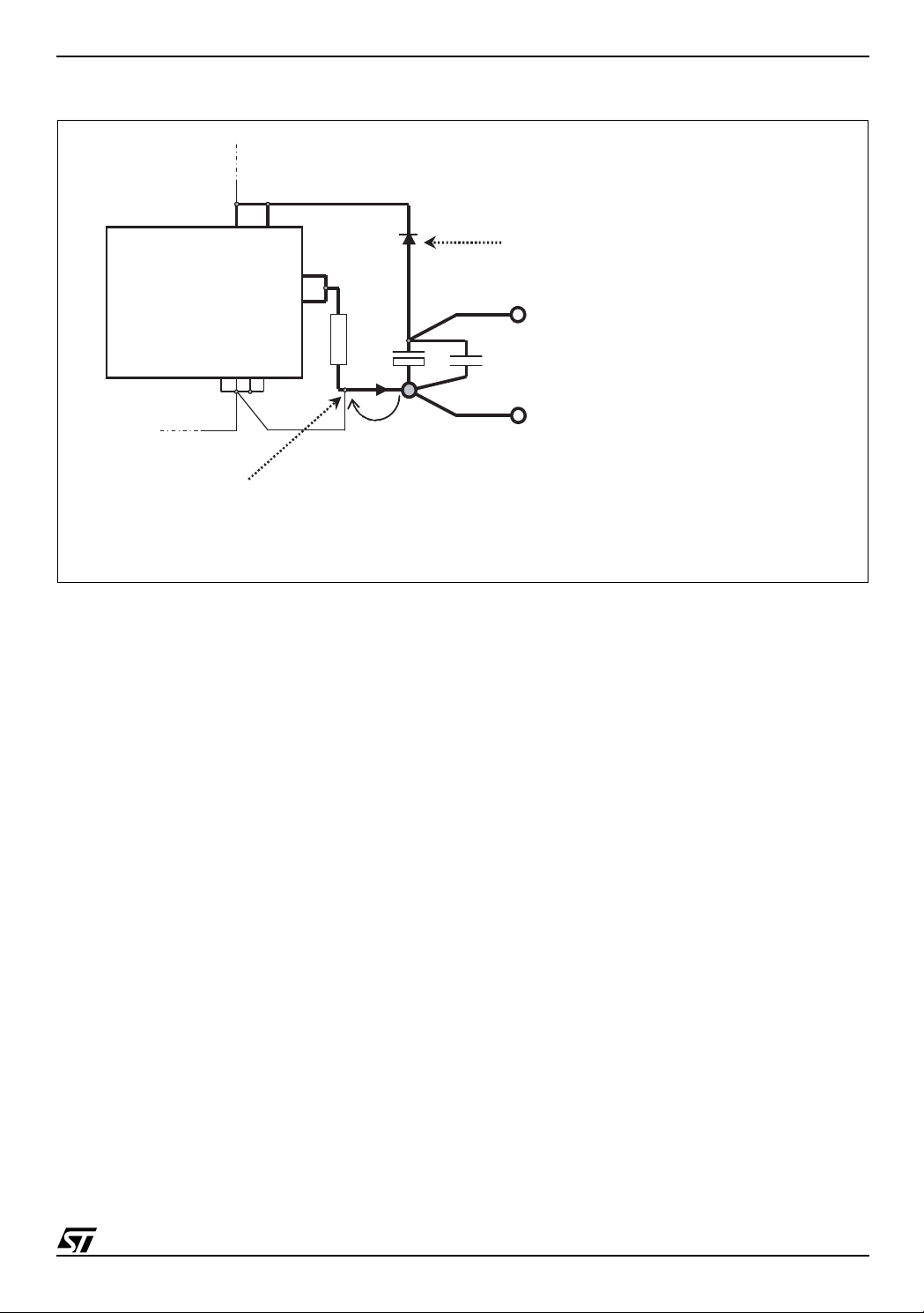
Figure 8. Two situations that must be avoided.
V
SA VSB
SENSE
A
SENSE
B
L6205, L6206, L6207
GND
GND
GND
GND
R5
C6
DON’T conne ct the Logic GND here
Voltage drop due to current in s ense
path can disturb lo gic GND.
AN1762 APPLICATION NOTE
DON’T put a di ode here!
Recircul at ing current cannot flow into t he
bulk cap ac itor and causes a high voltage
spike that c an des troy the I C .
+
C7
VS = 8 ÷ 52 V
-
3.5 S en sing Resistors
Each motor winding current is flowing through the corresponding sensing resistor, causing a voltage drop that
can be used, by the logic (integrated in the L6207; an external logic can be used with L6205 and L6206), to
control the peak value of the load current. Two issues must be taken into account when choosing the R
SENSE
value:
– The sensing resistor dissipates energy and provides dangerous negative voltages on the
SENSE
pin
during the current recirculation. For this reason the resistance of this component should be kept low.
– The voltage drop across R
parator (L6207 only). The lo wer is the R
on Vref pin and to the input offset of the current sense comparator: too small values of R
is compared with a reference voltage (on V
SENSE
value, the higher is the peak current error due to noise
SENSE
pin) by the internal com-
ref
must be
SENSE
avoided.
A good compromise is calculating the sensi ng resistor value so that the voltage drop , corresponding to the peak
current in the load (I
), is about 0.5 V: R
peak
SENSE
= 0.5 V / I
peak
.
It should be clear that sensing resistor must absolutely be non-inductive type in order to avoid dangerous negative spikes on
SENSE
pins. Wire-wounded resistors c annot be used here, whi le Metall ic film res istor s are recommended for their high peak current capability and low inductance. For the same reason the connections
between the
(see also the
SENSE
pins, C6, C7, VSA, VSB and
Layout Considerations
section).
GND
pins (see Figure 7) must be taken as short as possible
The average power dissipated by the sensing resistor is:
Fast Decay Recirculation: P
R
Slow Decay Recirculation: PR ≈ I
≈ I
rms
rms
2
2
· R
· R
SENSE
SEN SE
· D,
D is the duty-cycle of the PWM current control, I
is the r.m.s. value of the load current.
rms
9/53
AN1762 APPLICATION NOTE
Nevertheless, sensing resistor power rating should be chosen taking into account the peak value of the dissipated power:
where I
is the peak value of the load current.
pk
PRI
pk
2
R
⋅≈
SENSE
,
Using multiple resistors in parallel will help obtaining the required power rating with standard resistors, and reduce the inductance.
R
The following table shows R
tolerance reflects on the peak current error: 1% resistors should be preferred.
SENSE
recommended values (to have 0.5V drop on it) and power ratings for typical
SENSE
examples of current peak values.
I
pk
0.5 1 0.25
1 0.5 0.5 2 X 1Ω, 0.25W paralleled
1.5 0.33 0.75 3 X 1Ω, 0.25W paralleled
2 0.25 1 4 X 1Ω, 0.25W paralleled
R
SENSE
Value
[Ω]
R
SENSE
Power Rating
[W]
Alternatives
3.6 Charge pump external components
An internal oscillator, with its output at CP pin, switches from GND to 10V with a typical frequency of 600kHz
(see Figure 9).
Figure 9. Charge Pump .
VS + 10 V - VD1 - V
D2
f = 600 kHz
VS + 10 V - VD1
V
- VD1
S
C8
= 70Ω
= 70Ω
Charge Pump
Oscillator
10 V
5 V
10 V
f = 600 kHz
D1
V
BOOT CP
To High-Side
Gate Drivers
C5
R4
D2
V
10 V
SA VSB
R
DS(ON)
R
DS(ON)
L6205, L6206, L6207
When the oscillator output is at ground, C5 is charged by VS through D2. When it rises to 10V, D2 is r eve rse
biased and the charge flows from C
imum voltage of V
+ 10V - VD1 - VD2, which supplies the high-side gate drivers.
S
With a differential vol tage betw een V
ical current drawn by the V
BOOT
to C8 through D1, so the V
5
and V
S
of about 9V and both the bridges switching at 50kHz, the typ-
BOOT
pin is 1.85 mA.
pin, after a few cycles, reaches the max-
BOOT
10/53
AN1762 APPLICATION NOTE
Resistor R4 is added to reduce the maxi mum current i n the exter nal components and to reduce the slew rate of
the rising and falling edges of the voltage at the
circuit. For the same reason car e must be taken in realiz ing the PC B layout of
also the
Layout Considerations
section). Recommended values for the charge pump circuitry are:
D1, D2 : 1N4148
R4 : 100
Ω (1/8 W)
C5 : 10nF 100V ceramic
C8 : 220nF 25V ceramic
Due to the high charge pump frequency, fast diodes are required. Connecting the cold side of the bulk capacitor
(C8) to V
R4 = 100
instead of GND the average current in the external diodes during operation is less than 10 mA (with
S
Ω
); at startup (when VS is provided to the IC) is less than 200 mA while the reverse voltage is about
10 V in all condi tions. 1N4148 diodes withstand about 200 mA DC (1 A peak), and the maximum rever se voltage
is 75 V, so they should fit for the majority of applications.
3.7 S ha ring the Charge Pump Circuitry
If more than one device is used in the application, it's possible to use the charge pump from one L6205, L6206
or L6207 to supply the V
pins of several ICs. The unused CP pins on the slaved devices are left uncon-
BOOT
nected, as shown in Figure 10. A 100nF capacitor (C8) should be connected to the V
Supply voltage pins (V
) of the devices sharing the charge pump must be connected together.
S
The higher the number of devices sharing the same charge pump, the lower will be the differential volt age available for gate drive (V
- VS), causing a higher R
BOOT
In this case it's recommended to omit the resistor on the
charge pump circuitry.
Better performance can als o be obtained using a 33nF capacitor for C5 and using s chottky diodes (for ex ample
BAT47 are recommended).
Sharing the same charge pump ci rcuitr y fo r mor e than 3÷4 devi ces is not recommended, sinc e it wil l reduce the
V
voltage increasing the high-side MOS on-resistance and thus power dissipation.
BOOT
CP
pin, in order to minimize interferences with the rest of the
R4, C5, D1, D2
for the high side DMOS, so higher dissipating po wer.
DS(ON)
CP
pin, obtaining a higher current capability of the
connections (see
pin of each device.
BOOT
Figure 10. Sha ring the char ge pu m p c ir cui t ry .
To other Devices
V
BO OT
To High-Side
Gate Drivers
C18 = 100 nF
V
V
SA
CP
SB
L6205, L6206, L6207
D2 = BAT47
V
BOOT
To High-Side
Gate Drivers
D1 = BAT47
C5 = 33nF
CP
V
SA VSB
C8 = 100nF
L6205, L6206, L6207
11/53
AN1762 APPLICATION NOTE
3.8 Reference Voltage for PWM Current Control (L6207 ONLY)
The L6207 has two analog inputs, V
peak value of the motor curr ent through th e integrated PWM circuitry . In typical applications these p ins ar e connected together, in order to obtain the same cur rent i n the two m otor windings. A fixed reference vol t age can be
easily obtained through a resistive divider from an available 5 V voltage rail (maybe the one supplying the µC
or the rest of the application) and GND.
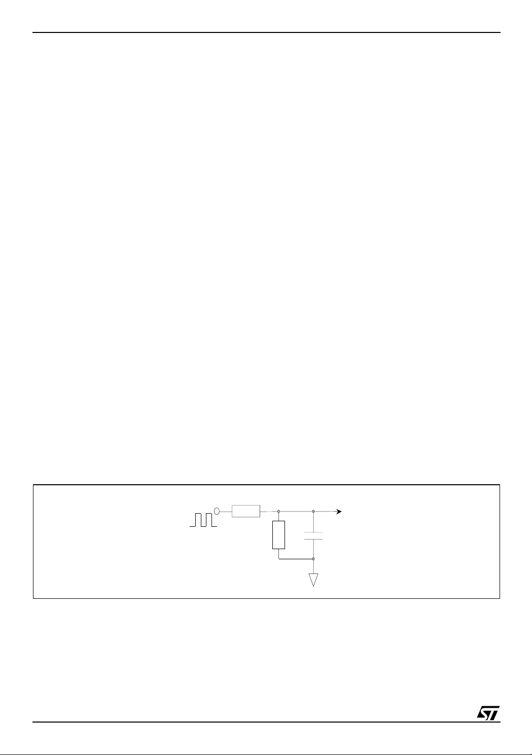
A very simple way to obtain a variable voltage without using a DAC is to low-pass filter a PWM output of a µC
(see Figure 11).
Assuming that the PWM output swings from 0 to 5V, the resulting voltage will be:
refA
and V
V
ref
, connected to the internal sense comparators, to control the
refB
5V DµCR
⋅⋅
-----------------------------------------=
R
LPRDIV
DIV
+
where D
Assuming that the µC output impedance is lower than 1k
is the duty-cycle of the PWM output of the µC.
µC
Ω,
with RLP = 56kΩ, R
= 15kΩ, CLP = 10nF and a
DIV
µC PWM switching fr om 0 to 5V at 100kHz , the l ow pass fi lter tim e consta nt is about 0.12 ms an d the remai ning
ripple on the V
voltage will be about 20 mV. Using higher values for RLP, R
ref
and CLP will reduce the ripple,
DIV
but the reference voltage will tak e more time to vary after changing the duty -cycle of the µC PWM, an d too high
values of R
As sensing resistor values are typically kept small, a small noise on V
will also increase the im pedance of the V
LP
net at low frequencies, causing a poor nois e immunity.
ref
input pins might cause a considerable
ref
error in the output current. It's then recommended to decouple these pins with cerami c capaci tors of some tens
of nF, placed very close to V
and GND pins. Note that V
ref
pins cannot be l eft unconnected, while, if connected
ref
to GND, zero current is not guaranteed due to voltage offset in the sense comparator. The best way to cut down
(IC) power consumption and clear the load current is pulling down the
age, PWM integrated circuitry can loose control of the current due to the minimum allowed duration of t
the
Programmable off-time Monostable
section).
EN
pins. With very small reference volt-
ON
(see
Figure 11. Obtaining a variable voltage through a PWM outpu t of a µC.
PWM Output
of a µC
R
LP
R
DIV
V
ref
C
LP
12/53
GND
AN1762 APPLICATION NOTE
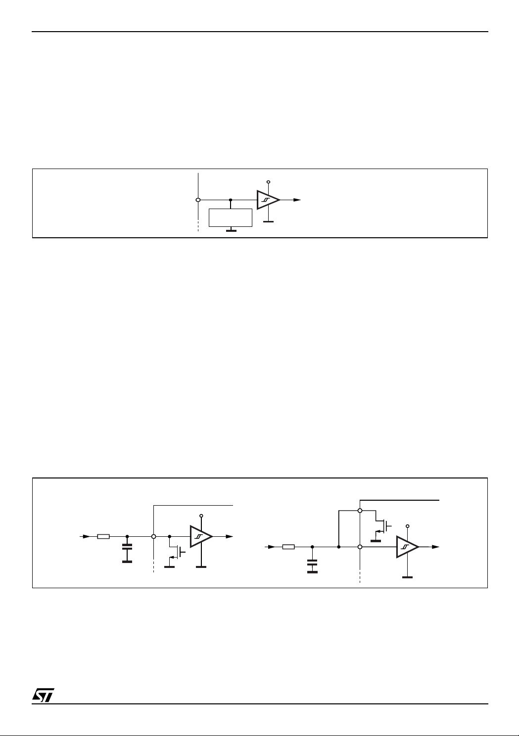
3.9 Input Logi c pin s
IN1A, IN2A, IN1B, IN2
teresis to ensu re the r equire d noise i mmuni ty. Typic al val ues for tur n-on and t urn-off thresh olds ar e V
V
= 1.3V. Pins are ESD prote cted (see Figur e 12) (2kV h uman-body ele ctro-static discharge), a nd can be d irectly
th,OFF
connected to t he logic o utp uts of a µC; a series resis tor is gen erall y not recom mende d, as it co uld hel p induct ed nois e
to disturb the inp uts. All logic pins enforce a speci fi c behavior and cannot be left unconnected.
Figure 12. Logic input pins.
3.10 EN pi ns
The
ENA, EN
pins are, actuall y, bi-directiona l: as an input, with a comparator si milar to the other logi c input pins (TTL/
B
CMOS with hysteresis), they control the state of the PowerDMOS. When each of the two pins is at a low logic level,
all the PowerDMOS of the corresponding H-bridge (A or B) are turned off. In L6205 and L6207 the EN pins are also
connected to the two corresponding open drain outputs of the protection circuits that will pull the pins to GND if over
current in the corresponding H-bridge or over temperature conditions exist. In L6206 the open drain outputs are on
separate pi ns, OCD
with L6205 and L6207 (and L6206 if EN pins are connected to DIAG pins) EN pins must be driven through a series
resistor of 2.2k
A capacitor (C
Ω
EN
value of the output current when overcurrent conditions persist (see
not be left unconnected.
are CMOS/TTL com patible logic i nput pins. The input compara tor has been realized with hys-
B
= 1.8V and
th,O N
5V
ESD
PROTECTION
D01IN1329
and OCDB, allowing easier external di agnostics an d overcurrent ma nagement. For this reason,
A
minimum (for 5V logic), to al low the voltage at the pin to be pulled below th e tur n-off threshold.
in Figure 13) connected between each EN pin and GND is also recommended, to reduc e the r.m.s.
Over Current Protection
section). EN pin must
Figure 13. ENA and ENB input pins .
L6205, L6207 L6206
PUSH-PULL
OUTPUT
R
EN
ENA or EN
ENA or EN
B
B
C
EN
EN
C
EN
OCDA or OCD
5V
PUSH-PULL
OUTPUT
R
ENA or EN
B
5V
B
13/53
AN1762 APPLICATION NOTE
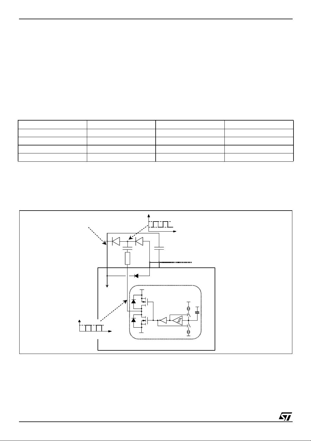
3.11 Programmable off-time Monostab le (L6207 ONL Y)
The L6207 includes a constant off time PWM current controller for each of the two bridges. The current control
circuit senses the bridge current by sensing the voltage drop across an external sense resistor connected between the source of the two lower power MOS transistors and ground, as shown in Figure 14. As the current in
the load builds up the voltag e across the sens e r esistor incr eases proportionally . W hen the vo ltage drop ac ross
the sense resistor becomes greater than the voltage at the reference input (VREF
parator triggers the monostable switching the low-side MOS off. The low-side MOS remain off for the time set
by the monostable and the motor current recirculates in the upper path. When the monostable times out the
bridge will again turn on. Since the internal dead time, used to prevent cross conduction in the bridge, delays
the turn on of the power MOS, the effective off time is the sum of the monostable time plus the dead time.
Figure 14. PWM Current Control Circuitry (L6207 ONLY).
VS
TO GATE LOGIC
BLANKING TIME
MONOST ABLE
1µs
FROM THE
LOW-SIDE
GATE DRIVERS
or VREFB) the sense com-
A
(or B)
A
5mA
MONOSTABLE
S
(0) (1)
5V
RC
C
OFF
R
Q
R
-
+
2.5V
A(or B)
OFF
RESET
BLANKER
SENSE
COMPARATOR
COMPARATOR
OUTPUT
DRIVERS
+
DEAD TIME
+
-
VREF
A(or B)
2H 1H
DRIVERS
+
DEAD TIME
2L 1L
SENSE
A(or B)
R
SENSE
OUT2
OUT1
I
OUT
A(or B)
A(or B)
D02IN1352
LOAD
(or B)
A
Figure 15 shows the typical operating waveforms of the output current, the voltage drop across the sensing resistor, the RC pin voltage and the status of the bridge. Immediately after the low-side Power MOS turns on, a
high peak current flow s through the sen sing resistor due to the rev erse recovery of the freewheeling diodes . The
L6207 provides a 1
µs
Blanking Time t
that inhibits the comparator output so that this current spike cannot
BLANK
prematurely re-trigger the monostable.
14/53
AN1762 APPLICATION NOTE
Figure 15. PWM Output Current Regulation Waveforms (L6207 ONLY).
I
OUT
V
REF
R
SENSE
V
SENSE
V
REF
0
V
RC
5V
2.5V
ON
OFF
SYNCHRONOUS RECTIFICATION
D02IN1351
t
OFF
1µs t
BLANK
Slow Decay Slow Decay
t
RCRISE
t
RCFALL
1µs t
DT
BC
t
ON
t
RCFALL
DDA
BC
t
OFF
1µs t
t
RCRISE
1µs t
BLANK
DT
Figure 16 shows the magnitude of the Off Time t
calculated from the equations:
t
RCFALL
t
OFF
where R
20K
0.47nF ≤ C
t
DT
= 0.6 · R
= t
RCFALL
and C
OFF
Ω ≤
R
OFF
OFF
OFF
= 1µs (typical value)
· C
OFF
· C
OFF
+ t
OFF
OFF
+ tDT = 0.6 · R
are the external component values and tDT is the internally generated Dead Time with:
≤ 100K
Ω
≤ 100nF
Therefore:
t
OFF(MIN)
t
OFF(MAX)
These values allow a sufficient range of t
The capacitor value chosen for C
The Rise Time t
= 6.6µs
= 6ms
RCRISE
to implement the drive circuit for most motors.
OFF
also affects the Rise Time t
OFF
will only be an issue if the capacitor is not completely charged before the next time the
monostable is triggered. Therefore, the on time t
versu s C
OFF
DT
, which depends by motors and supply parameters, has to
ON
OFF
RCRISE
and R
values. It can be approximately
OFF
of the voltage at the pin RCA (or RCB).
15/53
AN1762 APPLICATION NOTE
Ω
be bigger than t
can not be smaller than the minimum on time t
t
>1.5µs (typ. value)=
ONtON MIN()
t
ONtRCRISEtDT
RCRISE
= 600 · C
t
for allowing a good current regulation by the PWM stage. Furthermore, the on time t
RCRISE
ON(MIN)
.
–>
OFF
ON
3.11.1 Off-time Selection and mini mum on-time (L6207 ON LY)
Figure 16 also shows the lower limit for the on time tON for having a good PWM current regulation capacity. It
has to be said that t
smaller than t
RCRISE
is always bigger than t
ON
because the device imposes this condition, but it can be
ON(MIN)
- tDT. In this last case the device continues to work but the off time t
is not more con-
OFF
stant.
So, small C
switching frequency), but, the smaller is the value for C
value gives more flexibility for the applications (allows smaller on time and, therefore, higher
OFF
, the more influential will be the noises on the circuit
OFF
performance.
Figure 16. Off-time selection and minimum on-time (L6207 ONLY).
4
1.10
1.10
3
R = 100 kΩ
R = 47 k
R = 20 kΩ
10 0
to f f [ u s]
10
1
0.1 1 10 100
Coff [nF]
100
10
to n ( m in ) [ u s ]
1
0.1 1 10 100
Coff [nF]
16/53

AN1762 APPLICATION NOTE
minimum t
3.11.2 Slow Decay Mode (L6207 ONLY)
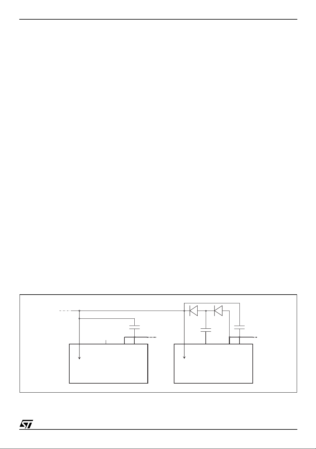
Figure 17 shows the operation of the bridge i n the Slow Decay mode. At the start of the off ti me, the lower power
MOS is switched off and the current recirculates around the upper half of the bridge. Since the voltage across
the coil is low, the current decays slowly. After the dead time the upper power MOS is operated in the synchronous rectification mode. When the monostable times out, the lower power MOS is turned on again after some
delay set by the dead time to prevent cross conduction.
Figure 17. Slow Decay Mode Output Stage Configurations
A) ON TIME B) 1µs DEAD TIME C) SYNCHRONOUS
D01IN1336
RECTIFICATION
D) 1µs DEAD TIME
In some conditions (short off-time, very low regulated current, high motor winding L / R) the system may need
an on-time shorter than 1.5µs. In these cases the PWM current controller can loose the regulation.
Figure 18 shows the operation of the circuit in this condition. When the current first reaches the threshold, the
bridge is turned off for a fixed tim e and the current decays. During the foll owing on-time current incr eases above
the threshold, but the bridge cannot be turned off until the minimum 1.5µs on-time expires. Since current increases more in each on-time than it decays during the off-time, it keeps growing during each cy cle, with steady
state asymptotic value set by duty-cycle and load DC resistance: the resulting peak current will be
I
= VS · D / R
pk
where D = t
ON
,
LOAD
/ (tON + t
) is the duty-cycle and R
OFF
is the load DC resistance.
LOAD
Figure 18. Minimum on-time can cause the PWM controller to loose the regulation (L6207 ONLY).
is about 1.5 µs
ON
V
/ R
ref
SENSE
needed tON is
than 1.5 µs
less
17/53

AN1762 APPLICATION NOTE
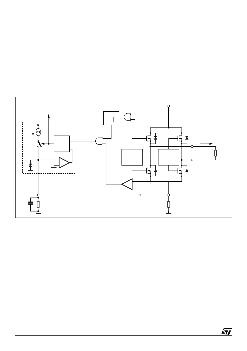
3.12 Over Current Protection
To implement an O ver Cur rent (i.e. shor t ci rcuit) Pr otection, a dedi cated Over Cur rent D etection (OCD) circ uitry
(see Figure 19 for a simplified schem atic) senses the current in each high side. P ower DMOS are actually made
up with thousands of individual identical cells, each carrying a fraction of the total current flowing. The current
sensing element, connected in parallel to the Power DMOS, is made only with few such cells, having a 1:N ratio
compared to the power DMOS. The total drain current is split between the output and the sense element according to the cell ratio. Sensed current is, then, a small fraction of the output current and will not contribute
significantly to power dissipation.
Figure 19. Over Current Detection simplified circuitry.
µC or LOGIC
+5V
L6205, L6207
POWER SENSE
1 cell
TO GATE
LOGIC
R
EN
EN
A
C
EN
R
40Ω TYP.
DS(ON)
INTERNAL
OPEN-DRAIN
POWER DMOS
OCD
COMPARATOR
OVER TEMPERATURE
L6206
POWER SENSE
1 cell
n cells
OUT1
I
/ n
1A
(I1A+I2A) / n
OUT1
VS
A
I
1A I2A
+
I
REF
VS
A
A
A
OUT2
OUT2
A
HIGH SIDE DMOSs OF
POWER DMOS
n cells
I
/ n
2A
A
HIGH SIDE DMOSs OF
THE BRIDGE A
POWER SENSE
1 cell
THE BRIDGE A
18/53
µC or LOGIC
+5V
I
1A I2A
POWER SENSE
1 cell
+
I
(I1A+I2A) / n
I
REF
I
REF
.
POWER DMOS
n cells
/ n
2A
1.2V
-
+
POWER DMOS
TO GATE
LOGIC
R
ENA
C
ENA
EN
OCD
A
A
R
DS(ON)
40Ω TYP.
INTERNAL
OPEN-DRAIN
n cells
OCD
COMPARATOR
OVER
TEMPERATURE
PROGCL
I
/ n
1A
A,
R
CLA

AN1762 APPLICATION NOTE
This sensed current is co mpar ed to an internall y generated refer ence (adj ustable through the exter nal resi stors
R
and
R
CLA
sum of the currents in the bridges 1A and 2A or 1B and 2B reaches the threshold (5.6A typical value for L6205
and L6207; adjustable through the external resistors
drain are inter nally connected to the
protection working. To ensure an over current protection, connect these pins to an external RC network (see
Figure 19).
Figure 20 shows the device operating in overcurrent condition (short to ground). When an over current is detected the internal open drain mosfet pull the
bridge and allowing the current to decay. Under a persistent over current condition, like a short to ground or a
short between two output pins, the external RC network on the
of the output current by imposing a fixed disable-time after each over current occurrence. The values of
and
C
are selected to ensure pr oper operation of the dev ice under a shor t circui t conditi on. When the curr ent
EN
flowing through the high side DMOS reaches the OCD threshold (5.6 A typ. for L6205 and L6207, adjustable for
L6206), after an internal propagation delay (t
voltage falls below the turn-off threshold (V
delay (t
D(OFF)EN
are
off
, there is no current flowing through them and no current to sense so the OCD circuit, after a short delay
(t
OCD(OFF)
reaches the turn-on threshold (V
Even if the maximum output current can be very high, the external RC network provides a disable time (t
to ensure a safe r.m.s. value (see Figure 20).
for L6206) to detec t an over current conditi on. A n i nternal open dr ain mosfet turns on when the
CLB
R
and
R
for L6206); in L6205 and L6207 the open
CLB
EN
pin (see Figure 19) reduces the r.m.s. value
C
. When the EN pin
EN
EN
pins; with L6206
EN
pin to GND switching off all 4 power DMOS of the interested
OCD(ON)
TH(OFF)
CLA
OCD
pins should be c onnected to EN pins to all ow the
) the open drain starts discharging
) all the Power DMOS turn off after the internal propagation
). The current begins to decay as it circulates through the freewheeling diodes. Since the D MOS
), switches the internal open drain device off, and
), after the t
TH(ON)
D(ON)EN
R
can charge
EN
C
. When the voltage at EN pin
EN
delay, the DMOS turn on and the current restarts.
R
DISABLE
EN
)
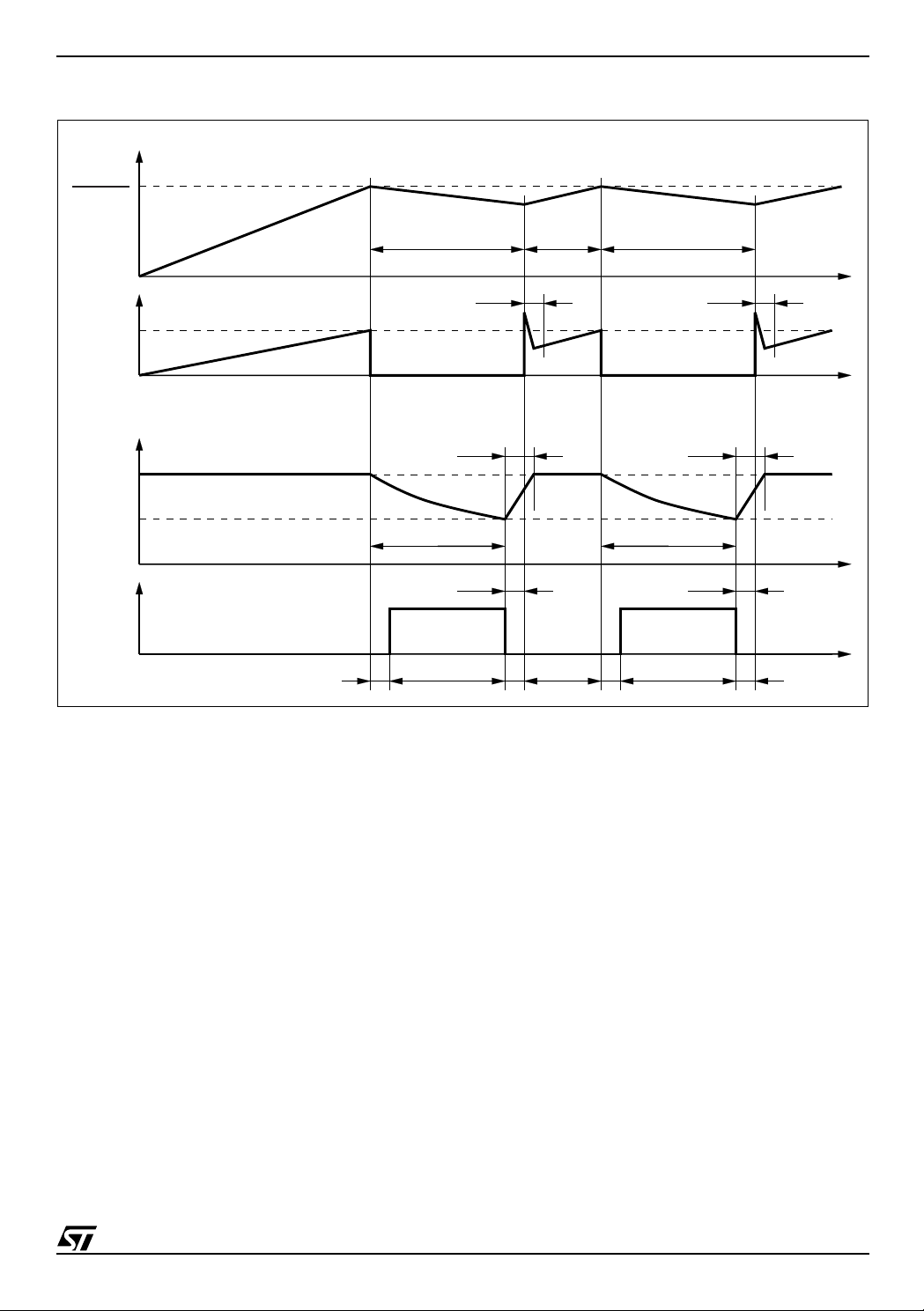
Figure 20. Over Current Operation.
t
DELAY
t
OCD(ON)
Outp ut Current
I
S OVER
t
EN(FALL)
t
D(OFF)EN
t
V
TH(OFF)
t
OCD(OFF)
DISABLE
EN
The maximum value reached by the current depends on its slew-rate, so on the short circuit nature and supply
voltage, and on the total intervention delay (t
). It can be noticed that after the first current peak, the max-
DELAY
imum value reached by the output current becomes lower, because the capacitor on
ing from a lower voltage, resulting in a shorter t
DELAY
.
The following approximate relations estimate the disable time and the first OCD intervention delay after the short
circuit (worst case).
t
DISABLE
V
TH(ON)
V
EN(LOW)
Ou tput Curr ent
t
D(ON)EN
t
EN(RISE)
EN
EN
pins is discharged start-
19/53

AN1762 APPLICATION NOTE
The time the device remains disabled is:
where
)(
tttt
++=
VV
−
CRt
⋅⋅=
ln
ENENRISEEN
−
VV
ENONDRISEENOFFOCDDISABLE
)()()(
)(
LOWENDD
)(
ONTHDD
V
EN(LOW)
The total intervention time is
where
t
OCD(OFF)
applied to R
The external RC network, C
t
DELAY
at least 100µs for t
The internal open drain can also be turned on if the device experiences an
The OVT will cause the device to shut down when the die temperature exceeds the OVT threshold
(T
J
all the Power DMOS will shut down, even if
falls below the OVT turn-off threshold (150 °C typ.), the open drain turn off,
then the PowerDMOS are turned on back.
is the minimum voltage reached by the EN pin, and can be estimated with the relation:
tt
−
eVV
⋅=
OFFTHLOWEN
)()(
+
CR
⋅
tttt
++=
V
)(
CRt ⋅⋅=
ln
ENOPDRFALLEN
V
, t
OCD(ON)
EN
) and a safe disable ti me (long t
>165 °C typ.). Since the OVT is also connected directly to the gate drive circuits (see Figure 1 to Figure 3),
.
, t
D(ON)EN
DISABLE
, t
D(OFF)EN
in particular, must be chosen obtaining a reasonable fast OCD intervention (short
EN
are recommended, keeping the delay time below 1÷2µs at the same time.
, and R
DISABLE
are device intrinsic parameters, VDD is the pull-up voltage
OPDR
). Figure 21 shows both t
EN
pin voltage is still over V
DISABLE
th(O FF )
)()(
OFFOCDENOFFD
ENOPDR
ENOFFDFALLENONOCDDELAY
)()()(
DD
)(
OFFTH
and t
over temperature
. When the junction temperature
C
is recharged up to V
EN
as a function of CEN:
DELAY
(OVT) condition.
TH(ON)
and
20/53

AN1762 APPLICATION NOTE
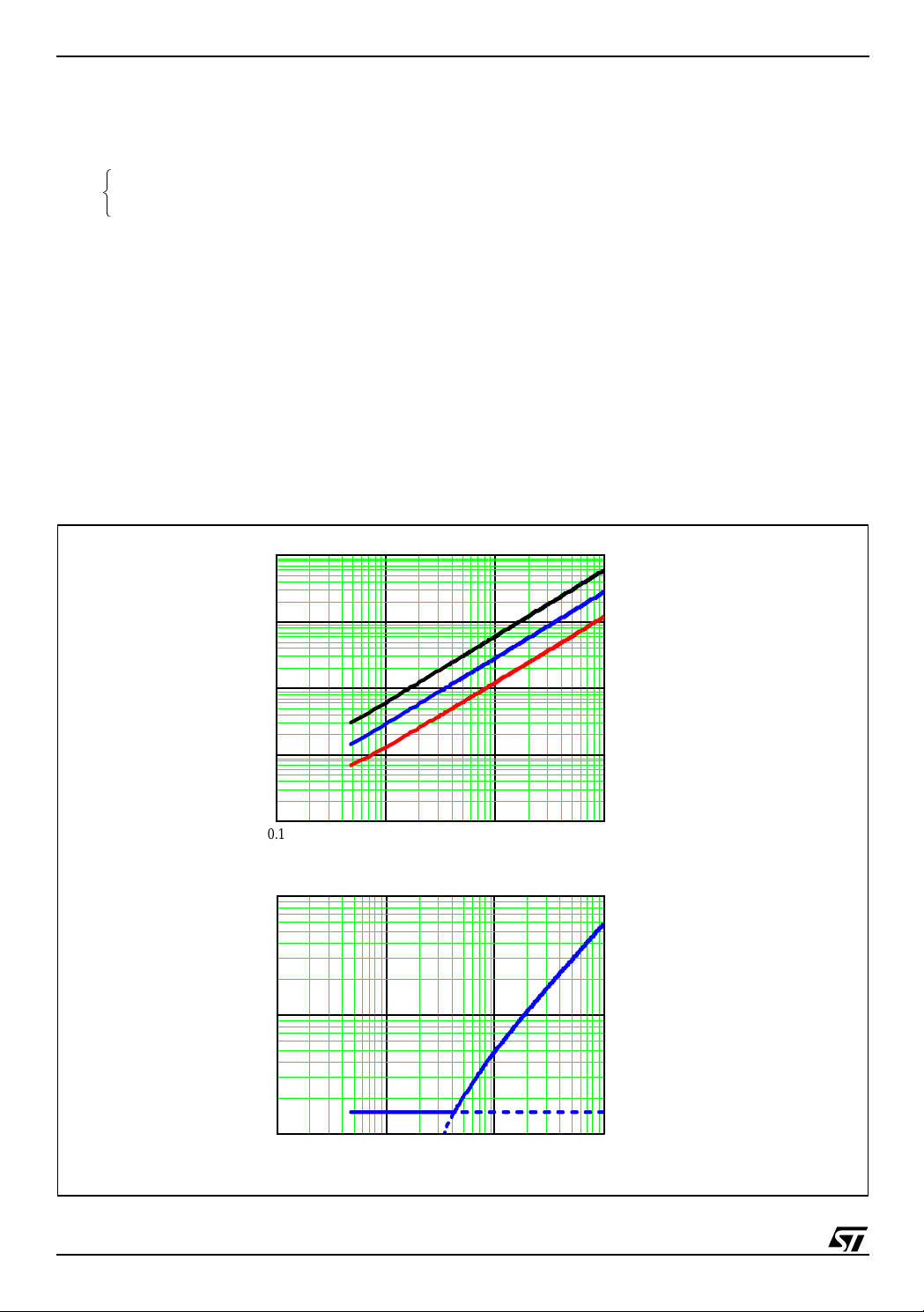
Figure 21. Typical disable and delay time as a function of CEN, for several values of REN.
1.10
3
100
REN = 220 kΩ REN = 100 kΩ
R
EN
R
EN
R
EN
= 47 kΩ
= 33 kΩ
= 10 kΩ
[µs]
DISABLE
t
10
1
110100
CEN [nF]
10
[µs]
1
DELAY
t
0.1
110100
CEN [nF]
3.13 Adjusting the Over Current Detection trip point (L6206 ONLY)
The L6206 allows the user to set the Over Current Detection threshold separately for the two full bridges connecting two resistors (R
) to pins
CL
PROGCL
and
A
PROGCL
. The OCD threshold (I
B
) follows the equa-
SOVER
tions:
–I
–I
= 5.6A ±30% at -25 °C < Tj < 125 °C if RCL = 0 Ω (
SOVER
22100
----------------
= ±10% at -25 °C < Tj < 125 °C if 5K
SOVER
R
CL
PROGCL
Ω <
RCL < 40k
connected to GND)
Ω
Figure 22 shows the OCD threshold versus RCL value in the range from 5kΩ to 40kΩ.
21/53

AN1762 APPLICATION NOTE
Figure 22. Output Current Detection Threshold versus RCL Value (L6206 ONLY)
I
SOVER
[A]
5
4.5
4
3.5
3
2.5
2
1.5
1
0.5
0
5k 10k 15k 20k 25k 30k 35k 40k
[
R
Ω
CL
]
The Over Current Detection threshold can also be adjusted through an external reference voltage, as shown in
Figure 23. The external reference v oltage source s hould be able to sink c urrent (about 300 µA maxi mum). Moreover, if supply voltage i s provided to the L6 206 before V
starts working with minimum OCD threshold (actually the capacitor placed at the bottom of R
start-up time with higher OCD threshold). V
can also be obtained through a PWM output of a µC, adding a
EXT
, and its EN pins are at a high logic level, the devi ce
EXT
allows a short
CL
series resistor to obtain a low-pass filter.
The OCD threshold (I
) follows the equation:
SOVER
18416.7 1.2V Vext–()
I
SOVER
---------------------------------------------------------- -
= ±10%, at -25 °C < Tj < 125 °C if 0.5 A < I
R
CL
SOVER
< 4.5 A
Figure 23. Adjusting the OCD Threshold through an external refer ence vo ltage (L6206 ONL Y )
L6206
22/53
V
= 0 ÷ 1.2 V
ext
PROGCL
A
R
CL

AN1762 APPLICATION NOTE
3.14 Paralleling two Full Bridges
3.14.1Paralleling two Full Bridges to get a single Full Bridge
The outputs of L6205, L6206, L6207 can be paralleled to increase the output current capability or reduce the
power dissipation in the device at a given current level. It must be noted, however, that the internal wire bond
connections from the di e to the power or sens e pins of the pac kage must carr y current i n both of th e assoc iated
half bridges (see Figure 24). When the two halves of one full bridge (for example OUT1
nected in parallel, the peak current rating is not increased since the total current mus t still flow t hrough one bond
wire on the power supply or sense pin. In addition, the over current detection senses the sum of the current in
the upper devices of each bridge (A or B) so connecting the two halves of one bridge in parallel does not increase the over current detection threshold.
Figure 24. VS and SENSE pins maximum current handling
2.8A rms
5.6A peak
SOURCED Current
OCD Threshold:
OUT1
+ I
OUT2
= 5.6A typ.
I
OVER
CURRENT
DETECTION
SOURCED Current
OCD Threshold:
OUT1
+ I
OUT2
= 5.6A typ.
I
OVER
CURRENT
DETECTION
BRIDGE A
BRIDGE B
VS
A
OUT1
A
OUT2
A
SOURCED:
I
OUT1
SENSE
A
2.8A rms
5.6A peak
VS
B
OUT1
B
OUT2
B
SOURCED:
I
OUT1
+ I
SENSE
B
+ I
OUT2
OUT2
= I
SUPPLY
< 2.8A rms, 5.6A pk.
= I
SUPPLY
< 2.8A rms, 5.6A pk.
BRIDGE A
BRIDGE B
and OUT2A) are con-
A
VS
A
SINKED:
I
OUT1
+ I
OUT2
= I
SENSE
OUT1
OUT2
2.8A rms
5.6A peak
SENSE
VS
B
A
A
A
< 2.8A rms, 5.6A pk.
SINKED:
I
OUT1
+ I
OUT2
= I
SENSE
OUT1
OUT2
2.8A rms
5.6A peak
SENSE
B
B
B
< 2.8A rms, 5.6A pk.
This configuration has to be used when two separate loads are driven, since the ICs has only two ENABLE inputs, one for the full bridge A and the other for the bri dge B. In this case pull ing to G ND one of the tw o ENABLE
pins will disable only one load (see Figure 25).
This configuration can also be used if a 5.6A OCD threshold is desired (instead of 11.2A).
Half Bridge 1 and the Half Bridge 2 of the Bridge A are connected in parallel and the same done for the Bridge
B as shown in Figure 25. In this configuration, the peak current for each half bridge is still limited by the bond
wires for the supply and sense pins so the dissipation in the device will be reduced, but the peak current rating
is not increased. Using this configuration with L6206, two separate resistors connected to pins
PROGCL
must be used. With L6207, two separate RC network should be used on RC pins. When two different
B
PROGCL
and
A
loads are driven (see Figure 25) by the two equivalent hal f bridges, two separa te sensing resi stors are needed,
while if the two equivalent half bridges drive two separate loads, they must be connected from the
V
(see Figure 25) to make the PWM current control working properly.
S
OUT
pins to
In this configuration, the resulting bridge has the following characteristics (typical values).
- Equivalent Device: FULL BRIDGE
- R
0.15Ω Typ. Value @ TJ = 25°C
DS(ON)
- 2.8A max RMS Load Current
- 5.6A OCD Threshold
23/53

AN1762 APPLICATION NOTE
Figure 25. Parallel connection with lower Over curr ent Thresho ld (L6205, L6206, L6207)
VS
P
P
C
P
VBOOT
SENSE
SENSE
OUT1
OUT2
OUT1
OUT2
C
P
VBOOT
SENSE
SENSE
OUT1
OUT2
OUT1
OUT2
VS
VCP
VS
VS
VCP
GND
GND
GND
GND
A
17
B
14
19
12
A
3
B
8
A
4
A
18
B
B
13
L6205
A
20
B
17
22
15
A
3
B
10
A
5
A
21
B
8
B
16
18
19
6
L6206
7
EN
A
20
R
EN
IN1
1
IN2
2
IN1
9
IN2
10
GND
16
GND
157
GND
6
GND
5
OCD
4
EN
23
OCD
9
EN
14
IN1
1
IN2
2
IN1
11
IN2
12
PROGCL
24
PROGCL
13
EN
B
A
A
B
B
A
A
B
B
A
A
B
B
A
B
EN11
C
EN
IN
A
IN
B
R
EN
C
EN
IN
A
IN
B
R
CLA
R
CLB
8-52V
8-52V
+
VS
GROUND
+
VS
GROUND
DC
POWER
-
SIGNAL
GROUND
DC
POWER
-
SIGNAL
GROUND
C
LOAD
LOAD
C
LOAD
LOAD
C
1
1
2
D
1
R
D
C
C
2
C
BOOT
BOOT
2
D
1
R
D
2
EN
24/53
8-52V
+
VS
GROUND
-
DC
POWER
SIGNAL
GROUND
VS
A
20
VS
P
C
P
VBOOT
SENSE
SENSE
OUT1
OUT2
OUT1
OUT2
VREF
VREF
VCP
B
17
22
15
A
3
B
10
A
5
A
21
B
8
B
16
A
24
B
13
C
1
VS
C
2
D
1
R
BOOT
SENSE
SENSE
D
2
C
R
R
LOAD
VS
LOAD
V
= 0 ÷ 1 V
REF
L6207
EN
A
23
R
EN
IN1
1
IN2
2
IN1
11
IN2
12
GND
16
GND
15
GND
6
GND
5
RC
4
RC
9
EN
B
A
A
B
B
A
R
A
B
R
B
EN14
C
EN
IN
A
IN
B
C
A
C
B

AN1762 APPLICATION NOTE
For some applications the recommended configuration is Half Bridge 1 of Bridge A paralleled with the Half
Bridge 1 of the Bridge B, and the same for the Half Bridges 2 as shown in Figure 26.
Figure 26. Parallel connection for highe r current (L6205 and L6206 ONLY)
VS
P
P
C
P
VBOOT
SENSE
SENSE
OUT1
OUT2
OUT1
C
P
VBOOT
SENSE
SENSE
OUT1
OUT2
OUT1
OUT2
GND
GND
GND
GND
VS
VCP
VS
VS
VCP
A
17
B
14
19
12
A
3
B
8
A
4
A
18
B
7
B
13
L6205
A
20
B
17
22
15
A
3
B
10
A
5
A
21
B
8
B
16
18
19
6
7
L6206
EN
B
11
EN
IN1
1
IN2
2
IN1
9
IN2
10
GND
16
GND
15
GND
6
GNDOUT2
5
OCD
9
EN
14
OCD
4
EN
IN1
1
IN2
2
IN1
11
IN2
12
PROGCL
24
PROGCL
13
R
EN
A
C
EN
A
A
B
B
B
B
A
A
C
A
A
B
B
A
R
B
R
CLA
CLB
EN20
IN1
IN2
R
EN
EN
EN23
IN1
IN2
VS
8-52V
VS
8-52V
+
DC
POWER
GROUND
-
SIGNAL
GROUND
+
DC
POWER
GROUND
-
SIGNAL
GROUND
C
C
LOAD
C
LOAD
2
D
1
R
D
C
C
2
C
BOOT
BOOT
2
D
1
R
D
2
1
1
This configuration cannot be used with L6207, because of its internal PWM current controllers that work separately for bridge A and bridge B. Using this configuration with the L6207 may damage the device.
In this configuration the resulting Bridge has the following characteristics (typical values).
- Equivalent Device: FULL BRIDGE
- R
0.15Ω Typ. Value @ TJ = 25°C
DS(ON)
- 5.6A max RMS Load Current
- 11.2A OCD Threshold
It should be noted that using two separate loads for the two equivalent half br idges the maximum current cannot
be sourced or sinked simultaneously by the two equivalent half bridges (for example to drive two separate
loads), due to the 5.6 A maximum current limit for
driven (see Figure 26) R
CLA
and R
resistors connected to PROGCL pins of L6206 should have the same
CLB
SENSE
S
pins (see Figure 24). When a single load is
V
and
value.
25/53

AN1762 APPLICATION NOTE
3.14.2Paralleling the four Half Bridges to get a single Half Bridge
It is also possible to parallel the four Half Bridges to obtain a simple Half Bridge as shown in Figure 27.
This configuration cannot be used with L6207, because of its internal PWM current controllers that work sepa-
rately for bridge A and bridge B. Using this configuration with the L6207 may damage the device.
The resulting half bridge has the following characteristics (typical values).
- Equivalent Device: HALF BRIDGE
- R
- 5.6A max RMS Load Current
- 11.2A OCD Threshold
With L6206 R
Figure 27. Paralleling the four Half Bridges (L6205 and L6206 ONLY)
0.075Ω Typ. Value @ TJ = 25°C
DS(ON)
CLA
VS
8-52V
and R
+
DC
POWER
GROUND
-
SIGNAL
GROUND
resistors connected to PROGCL pins must have the same value.
CLB
C
1
VS
A
17
VS
P
VCP
C
P
VBOOT
SENSE
SENSE
OUT1
OUT2
OUT1
OUT2
B
19
12
A
3
B
8
A
4
A
18
B
7
B
13
L6205
C
2
D
1
R
D
C
LOAD
BOOT
2
EN
B
1114
EN
IN1
1
IN2
2
IN1
9
IN2
10
GND
16
GND
15
GND
6
GND
5
R
EN
A
C
EN
A
A
B
B
EN20
IN
26/53
VS
8-52V
+
DC
POWER
GROUND
-
SIGNAL
GROUND
VS
A
20
P
VCP
C
P
VBOOT
SENSE
SENSE
OUT1
OUT2
OUT1
OUT2
GND
GND
GND
GND
B
17
22
15
A
3
B
10
A
5
A
21
B
8
B
16
18
19
6
L6206
7
C
1
C
2
D
1
R
D
C
LOAD
BOOT
2
23
14
11
12
24
13
4VS
9
1
2
OCD
A
EN
A
OCD
B
EN
B
IN1
A
IN2
A
IN1
B
IN2
B
PROGCL
PROGCL
R
EN
C
EN
A
R
CLA
B
R
CLB
EN
IN

AN1762 APPLICATION NOTE
3.15 Power Management
Even when operating at current l evels well below the maxi mum ratings of the devi ce, the operating juncti on temperature must be kept below 125 °C.
Figure 28 shows the IC dissipated power versus the r.m.s. load current, in the case of a single IC driving two
loads (for instance 2 DC motors or a two-phase stepper motor) or a single IC, with two full bridges paralleled
(see
Paralleling two Full Bridges
phase stepper motor) and assuming the supply voltage is 24V.
Figure 28. IC Dissipated Power versus Output Current.
10
8
section
) driving one load (for instance 1 DC motor or one phase of a two-
6
2 Full Bridges
driving two loads
PD [W]
4
2
2 Full Bridges Pa ralleled
driving one load
0
0 0.5 1 1.5 2 2.5 3
I
[A]
OUT
3.15.1 Maximum output current vs. selectable devices
Figure 29 reports a performance comparison between different devices of the PowerSPIN family, for different
packages and in paralleled configuration, with the following assumptions:
- Each equivalent full bridge drives a load.
- Supply voltage: 24 V; Switching frequency: 30 kHz.
- T
= 25 °C, TJ = 125 °C.
amb
- Maximum R
- Maximum quiescent current I
- PCB is a FR4
(taking into account process spread) has been considered, @ 125 °C.
DS(ON)
(taking into account process spread) has been considered.
Q
with a dissipating copper surface on the top side of 6 cm2 (with a thickness of 35 µm) for
SO and PowerDIP packages (D, N suffixes).
- PCB is a FR4
with a dissipating copper surface on the top side of 6 cm2 (with a thickness of 35 µm ), 16
via holes and a ground layer for the PowerSO package (PD suffix).
- For each device configuration (on the x axis) y axis reports the maximum output (load) current.
- 2 x ’device’ means that the two loads are driven by two equivalent full bridges obtained par alleling two full bridges for each of the two IC used. The current reported in Figure 29 is the maximum output current an equivalent
full bridge (a paralleled IC).
No PWM
f
= 30 kHz (synch. slow decay)
SW
27/53

AN1762 APPLICATION NOTE
2
x
L
6
2
2
X
N
Figure 29. Maximum output current vs. selectable devi ces.
3.00
2.50
2.00
Load Current
1.50
[A]
1.00
0.50
N
D
X
2
2
6
L
D
X
2
2
6
L
L
D
P
X
X
2
2
6
X N
0
0
2
2
6
6
L
L
L
D
D
P
X
2
X
2
0
6
2
L
6
x
2
D
D
N
P
X
X
0
2
2
2
6
6
L
x
L
x
2
x
2
2
D
P
X
0
X
2
0
6
2
L
6
L
x
2
3.15.2 Power Dissipation Formulae for different sequences
Figure 30 to Figure 33 are screenshots of a spreadsheet that helps calculating power dissipation in specified
conditions (application and motor data), and estimates the resulting junction temperature for a given package
and copper area available on the PCB [4].
The model assumes that the device is d riving a two-phase bipolar stepper motor and that a PWM current c ontrol
with slow decay recirculation technique is implem ented (L6207 integrates the PWM controller); it considers power dissipation during the on-time and the off-time, rise and fall time (when a phase change occurs) considering
the operating sequence (N ormal, Wave or Half Step Mode) , the switching losse s and the quiesc ent current power dissipation.
28/53

AN1762 APPLICATION NOTE
"SLOW " = Synch ronous Slow D ecay
"FAST" = Qu asi-Synchronous Fast decay
s
Figure 30. Definition of parameters for the three different sequences. The current in only one phase
is shown.
NORMAL
I
I
pk
T
r
Figure 31. Input Data.
WAVE
T
∆∆∆∆I
I
load
t
T
load
T
f
I
T/2
∆∆∆∆I
I
I
pk
load
t
T
r
T
load
T
f
HALF STEP
I
I
pk
T
r
T
∆∆∆∆I
I
load
t
T
load
T
f
Input D ata
Device Input Values
Maximum D rain-Source ON R esistance Ron = 5.60E-01 [Ohm] Average Value between H igh-Side and Low-Side
Maximum diode voltage Vd = 1.20E+00 [V]
Quiescent Current Iq = 5.50E-03 [mA]
Motor Input Value
Maximum BEMF Voltage Vb = 1.50E+01 [V]
Mo to r In ductanc e Lm = 7.90E -0 3 [H]
Motor Resistance Rm = 6.60E+ 00 [Ohm]
Application Input Values
Supply Voltage Vs = 2.40E+01 [V]
Peak Current Ipk = 1.00E+00 [A]
Off-Time tOFF = 1.50E-05 [s]
Step Frequency fCK = 1.00E+03 [Hz]
Sensing Resistance Rs = 5.00E-01 [Ohm]
Decay Type -
Stepping sequence - "NORM A L", "HALF" or "WA VE "
SLOW
WAVE
29/53

AN1762 APPLICATION NOTE
Figure 32. Power Dissipation formulae and results.
Result
PowerDMOS
Commutation
Time
Tcom =
9.60E-08 [s] Vs / (250V/µs)
Rise Ti m e Trise =
Fall Time Tfall =
4.03E-04 [s]
3.16E-04 [s]
Duty Cycle D = 6.25E-01 -
Switching
Frequency
Current Ripple
Period T =
Load Time
Tload =
2.50E+04
fSW =
∆I = 2.85E-02 [A] (Vs - Vb)*D / (Lm* fSW)
2.00E-03 [s]
5.97E-04 [s]
Average Cur-
rent during
I =
9.86E-01 [A]
Load Time
r.m.s. Current
during Load
Irms =
9.86E-01 [A]
Time
Rise Tim e
Dissipating
Erise =
1.50E-04 [J]
Energy
[Hz]
Ipk Rm 2 Ipk Ron Ipk Rs Vs+⋅–⋅⋅–⋅–()
---------------------------------------------------------------------------------------------------------------
-------------------------------------------------------------------------------------------------------------
Ipk Rm 2+ Ipk Ron Ipk Rs Vs+⋅+⋅⋅⋅()
-------------------------------------------------------------------------------------------
Ipk Rm Ipk Rs Vs 2 Vd⋅–+⋅+⋅()
Vs
Vs
Vs 2 Vd⋅–()
-------------------------------------------------------
⋅ln–
Lm
--------------------------------------------- -
⋅ln–
Rm Rs 2Ron++
Lm
NORMAL Mode
Rm 2 Ron Rs+⋅+()
Lm
----------------------------
⋅ln–
Rm Rs+()
HALF or WAVE
Mode
Vb / Vs Sync. Slow Decay
(1-D) / tOF F
2 / fCK
4 / fCK
2 / fCK
T-Trise-Tfall
(3/4)T-rise
(T/2)-Trise
I∆
Ipk
-----–
2
2
I
2
Trise
---------------
3
∆
-------+⋅
3
Ipk Ipk I∆–()
2Ron Ipk
⋅⋅
NORMAL Mode
HALF Mode
WAVE Mode
NORMAL Mode
HALF Mode
WAVE Mode
Fall Time
Dissipating
Energy
Load Time
Diss. Energy
30/53
Efall =
Eload =
3.62E-04 [J]
6.50E-05 [J]
2Ron Ipk
2VdTfall
Ipk Rm Ipk Rs Vs 2 Vd⋅–+⋅+⋅()
⋅⋅
2Ron · Irms
3
Vs– 2Vd⋅+()
--------------------------------------
Rm Rs+()
---------------------------------------------------------------------------------
2
· Tlo a d
+⋅⋅
1
Lm
T–fall
----------------
Rm Rs+()
Rm Rs+()⋅exp–
2
Tfall
2
-------------
⋅⋅
MORMAL Mode
HALF or WAVE
Mode
Sync. Slow Decay

AN1762 APPLICATION NOTE
g
53.36
14.00
g
103.60
Commutatiion
Dissipating Pw
Quiescent
Dissipating Pw
Tot al Di ssi-
pating Power
Time
Ecom =
Pq = 1.32E-01
P =
6.78E-05 [J] 2Vs · I · Tcom · Tl oad · fSW
[W]
1.36E+00
[W]
Figure 33. Thermal Data inputs and results.
Packa
Copper Area 4.0 1÷10 sq. cm
Copper Area is on Same side of the device
Ground Layer N/A
Ambient Tem perature 50 -25 ÷ 100 ºC
e
Vs · Iq
2
---
·(Erise + Efall + Elo ad + E co m ) + P q
T
Input Data
SO24
Results
Thermal Resistance
Junction to Ambient
Thermal Resistance
Junction to Pins / Slug
Estim ated J un ction
Temperature
Estim ated
Pins / Slu
Temperature
ºC / W
ºC / W
122.66 ºC
31/53

AN1762 APPLICATION NOTE
4 APPLICATION EXAMPLE (L6207) Application Data Motor Data
Rotation Speed: 300 rpm (fCK= 1kHz) Winding Resistance: 6.6
Winding peak Current: 1A Winding Inductance: 7.9mH
Maximum Ripple: 50mA Step Angle: 1.8°/step
Supply Voltage: 24V ±5% Maximum BEMF at 300rpm: 15V
Sequence: Wave Mode
4.1 Decay mode, sensing resistors and reference voltag e.
Referring to approximated formulae i n Figure 32, it's poss ible to calcula te the Duty-Cycle (D), the S witching Frequency (f
D
≅
63%, fSW ≅ 25kHz, ∆I ≅ 29mA. The on-time is tON = D / fSW ≅ 25µs, which is far from the minimum allowed
), the Current Ripple (∆I). With a 15 µs off-time, we will have:
SW
(1.5µs), so slow decay can be used.
≅
The bulk capacitor need to withstand at least 24V + 5% + 25%
32V. A 50V capacitor will be used. Allowing a
voltage ripple of 200mV, the capacitor ESR should be lower than 200mV / 1A = 200m
bility should be about 1A.
Providing a reference voltage of 0.5V, 0.5
2
≅
I
rms
· R
· D ≅ 0.32W. Two 1Ω - 0.25W - 1% resistors in parallel are used. The charge pump uses rec-
SENSE
ommended components (1N4148 diodes, ceramic capacitors and a 100
R = 18k
Ω
, C = 1.2 nF are connected to the RC pins, obtaining t
have been placed, and the pins are driven by the µC through 100k
Ω
sensing resistor are needed. The re sistor s power rating i s abo ut P
Ω
resistor to reduce EMI).
≅ 16µs. On the EN pins 5.6nF capacitors
OFF
Ω
resistors. With these values, in case of
short circuit between two OUT pins or an OUT pin and GND, the PowerDMOS turns off after about 1µs, and
t
DISABLE
≅ 240µs.
Ω
Ω
; the AC current capa-
R
Figure 34. Application Example.
2-Phase
Stepper Motor
+
Logic Supply
5 V
-
18 kΩ 0.25 W
1%
2 kΩ 0.25 W
1%
µC
or
Custom Logic
= 0.5 V
V
ref
100 kΩ
100 kΩ
5.6 nF
Ceramic
5.6 nF
Ceramic
1N4148 1N4148
100Ω
0.25W
OUT
1B
2B
L6207
1.2 nF
Ceramic
V
BOOT
18 kΩ
5%
RC
OUT
OUT
OUT
1A
2A
IN1
A
IN1
B
IN2
A
IN2
B
EN
A
EN
B
V
V
refB RCA
refA
47nF
Ceramic
18 kΩ
5%
V
SA VSB
SENSE
SENSE
220nF 50V
Ceramic
A
B
100µF 50V
ESR<200mΩ
100nF 50V
Ceramic
+
10nF 50V
Ceramic
CP
VS = 24 V
4 X
1 Ω, 0.25 W, 1%
GND GND
B
1.2 nF
Ceramic
GND GND
-
With Wave Drive selected, referring to Figure 31 to Figure 33, the dissipating power is about 1.36 W. If the ambient temperature is lower than 50°C , with 4cm
2
of copper area on the PCB and a SO24 package, the estimated
junction temperature is about 123°C. Using more copper area or a PowerDIP package will reduce the junction
temperature.
32/53

AN1762 APPLICATION NOTE
5 APPENDIX - EVALUATION BOARDS
5.1 PractiSPIN
PractiSPIN is an evaluation and demonstratio n system that can be used with the Power SPIN family (L62X X) of
devices. A Graphical User Interface (GUI) (see Figure 35) program runs on an IBM-PC under windows and communicates with a common ST7 based interface board (see Figure 36) through the RS232 serial port. The ST7
interface board connects to a device spec ific ev aluation board (t arget board) via a standard 34 pin ribbon c able
interface.
Depending on the target device the PractiSPIN can drive a stepper motor, 1 or 2 DC motors or a brushless DC
(BLDC) motor, operatin g signific ant parameters such as SPEED, CURREN T, VOLTAGE, DIRECTIO N, ACCELERATION and DECELERATION RATES from a user friendly graphic interface, and programming a sequence
of movements.
The software also allows evaluating the power dissipated by the selected device and, for a given package and
dissipating copper area on the PCB, estimates the device's junction temperature.
Figure 35. PractiSPIN PC Soft w a re
33/53

AN1762 APPLICATION NOTE
Figure 36. PractiSPIN ST7 Ev al uat ion Board
5.2 EVAL6205N
An evaluation board has been produced to help the evaluation of the device in PowerDIP package. It implements a typical application with several added components. Figure 38 shows the electrical schematic of the
board; in the table below the part list is reported.
CN1, CN2, CN3, CN4 2-poles connector R1 100Ω resistor
CN5 34-poles connector R2 700
C1 220nF/100V Ceramic or Polyester capacitor R3, R4, R13 10k
C2 220nF/100V Ceramic or Polyester capacitor R5, R6 4.7k
C3 100µF/63V capacitor R7, R8, R9, R10, R11, R12 1
C4 10nF/100V Ceramic capacitor R18, R14 1k
C5 10µF/16V Capacitor R15, R19 20k
C6, C7, C11 100nF Capacitor R16, R20 2.2k
C8, C10 470pF Capacitor R21, R17 5k
C9, C12 68nF Capacitor R22 12k
C13 2.2nF Capacitor R23 50k
D1, D2 1N4148 Diode U1 L6205N
D3 BZX79C5V1 5.1V Zener Diode U2 L6506
JP1 3-pin jumper JP2, JP3, JP4, JP5 2-pin jumper
Ω 0.6W resistor
Ω resistor
Ω resistor
Ω 0.4W resistor
Ω resistor
Ω resistor
Ω resistor
Ω trimmer
Ω resistor
Ω trimmer
The Evaluation Board provides ex ternal connectors for the supply voltage, an exter nal 5V reference for the logi c
inputs, four outputs for the motor and a 34-pin connector to control the main functions of the board through an
external
R23 sets the PWM operating frequency. If the L6506 does not need to be used, simply connect the two V
µ
C board or the PractiSPIN tool. The board also accommodates the L6506 PWM current controller.
REF
inputs to a voltage high enough to keep current control inactive.
The PractiSPIN tool is composed of a graphic interface software running on a PC that connects with the hard-
ware based on the ST7 µC, which contains an upgradeabl e firmware. This tool allows a fast and easy eval uation
of the PowerSPIN family devices, giving the ability of driving DC, BLDC and Stepper motors, depending on the
target device. The PractiSPIN
connected to the EVAL6205N can drive DC mo tors and inducti ve loads , allowing
output voltage and current settings
The PC-software also provides a Po wer Dissipa tion and Ther mal Analysi s secti on, intended to help a fas t eval-
uation of the device, package and dissipating copper area required by the user’s application, and to be a good
starting point designing an application (from the power dissipation and thermal point of view).
34/53

AN1762 APPLICATION NOTE
Running the evaluation board in stand-alone mode, instead, R17 and R21 set the reference voltage separately
for the two bridges, while R16, C9 and R20, C12 are low-pass filters to provide an external reference voltage
by a PWM output of a
can be disconnected through JP4 and JP5, unless the PractiSPIN ST7 evaluat ion board is used. This board, in
fact, is provided with an offset cancellation circuitry trimmable through a potentiometer (see PractiSPIN documentation).
Closing JP2 and JP3 is recommended for safe Over Current Protection.
The 5V voltage for logic inputs and for references (V
supply voltage, the value of resistor R2 should be changed in order to ensure a correct biasing of D3.
The jumper JP1 allows choosing the 5V voltage from the internal zener diode network or pin 11 of CN5 (for ex-
ample an external µC board can provide 5V to the evaluation board). Also CN2 connector can be used to provide an external 5V voltage to the board (in that case R2, D3 should be disconnected). CN2, or pin 1 of CN5,
can also be used to provide a 5V voltage to external circuits (as, for example, the PractiSPIN ST7 board). In this
case the current that can be drawn form the board depends on the supply voltage and on R2 value.
Figure 39 to Figure 41 show the component placement and the tw o layers layout of the L6205N Evaluation
Board. A large GND area has b een used, to guar antee minimal noise and good p ower dissipation for the device.
Figure 37. EVAL6205N.
µ
C (see also the Microste pping sec tion) . Using e xternal V
refA
and V
) is obtained from R2, D3. Depending on the
refB
inputs R15, R17, R19, R21
REF
R21
JP1
R3
R5
JP2
C6
JP5
JP4
R17
R4
R6
JP3
C7
5.2.1 Important Notes
JP1 : close in INT position for use with PractiSPIN ST7 board
C6, C7 : recommended change to 5.6 nF for safe Overcurrent protection
R3, R4 : recommended change to 100 k for safe Overcurrent protection
R5, R6 : recommended change to 100 k if EN pins are driven from the CN5 connector (for example with Prac-
tiSPIN ST7 board) for safe Overcurrent protection
R17, R21 : set the maximum current obtainable through PractiSPIN (see PractiSPIN documentation)
R2 : recommended change to adequate value (depending on supply voltage) to obtain 5V across D3
JP2, JP3 : close for safe Overcurrent protection
JP4, JP5 : close for use with PractiSPIN ST7 board
35/53

AN1762 APPLICATION NOTE
Figure 38. EVAL6205N Electrical schematic.
CN1
2
VCCREF
CN3
CN2
1
1
R2
2
GND
D3
C5
JP1
int.
2
PullUp
13
ext.
+5V
C3
14
VSB
CN4
1
2
2
18
4
OUT1B7OUT2A
OUT 1A
LIMI T_B
1
INT3
INT0
INT2
INT6
246810121416182022242628303234
13579
ADC_REF
PullUp
13
OUT 2B
IN1
ENA
LIMIT_A
IN4
TOUTB0 P2.3
TOUTPB1 2.7
TINA0 P2.0
TINB0 P2.1
1113151719212325272931
+5V
R15
PullUp
U1
L6205
TINB1 P2.5
IN3
TOUTA1 P2.6
IN2
ENB
TINA1 P2.4
33
OCMPA1 P4.2
OCMPB1/ICAP B1 P4.3
VREFA
R17
VREF_A
PullUp
R19
VREF_B
R20
R16
C9
C12
CN5
VREFB
JP4
CW
9
GND
17
Vref 2
Osc_Out
Vref 116Sync
15
Vsens e2
10
Vsens e1
4
EN
11
Out4
12
Out3
Out2
Out1
VCC
13
14
PullUp
SENSE_B
SENSE_A
_4
_3
_2
_1
R13
18
R/C
In4
In3
In2
In1
C11
JP5
U2
L6506Dip
2
3
1
8
7
6
5
CW
R21
C13
R23
IN4
IN3
IN2
IN1
PullUp
CW
R22
36/53
17
VSA
D2
C4
R1
D1
C1
C2
PullUp
19
VCP
12
VBOOT
15
GND
16
GND
6
GND
5
GND
IN11IN2
R4
R3
_1
ENB
ENA
IN3
11
20
2
R6
R5
_2 ENA LIMIT_A
_3 LIMIT_B
ENB _4
9
SENSEB
SENSEA
IN4
10
8
3
JP3
JP2
1
2
3
4
R12
R11
R10
R9
R8
R7
C6
C7
R14
C8 C10
SENSE_A SENSE_B
R18

Figure 39. EVAL6205N Component placement.
AN1762 APPLICATION NOTE
Figure 40. EVAL6205N Top Layer Layout.
Signal GND
Power GND
(Bulk Capacitor)
37/53

AN1762 APPLICATION NOTE
Figure 41. EVAL6205N Bottom Layer Layout.
Short SENSE
Paths
38/53

AN1762 APPLICATION NOTE
5.3 EVAL6206N
An evaluation board has been produced to help the evaluation of the device in PowerDIP package. It implements a typical application with several added components. Figure 43 shows the electrical schematic of the
board; in the table below the part list is reported.
CN1, CN2, CN3, CN4 2-poles connector R1 100Ω resistor
CN5 34-poles connector R2 700
C1 220nF/100V Ceramic or Polyester capacitor R3, R4, R16 10k
C2 220nF/100V Ceramic or Polyester capacitor R5, R6 4.7k
C3 100µF/63V capacitor R7, R8 50k
C4 10nF/100V Ceramic capacitor R9, R10, R11, R12, R13, R14 1
C5, C8, C10 10µF/16V Capacitor R15, R21 2.2k
C6, C7 47nF Capacitor R17, R23 20k
C9, C13 68nF Capacitor R18, R22 750
C11 100nF Capacitor R19, R25 2.2k
C12, C14 470pF Capacitor R20, R26 5k
C15 2.2nF Capacitor R27, R24 1k
D1, D2 1N4148 Diode R28 12k
D3 BZX79C5V1 5.1V Zener Diode R29 50k
JP1 3-pin jumper U1 L6205N
JP2 to JP7 2-pin jumper U2 L6506
Ω 0.6W resistor
Ω resistor
Ω resistor
Ω trimmer
Ω 0.4W resistor
Ω resistor
Ω resistor
Ω resistor
Ω resistor
Ω trimmer
Ω resistor
Ω resistor
Ω trimmer
The Evaluation Board provides ex ternal connectors for the supply voltage, an exter nal 5V reference for the logi c
inputs, four outputs for the motor and a 34-pin connector to control the main functions of the board through an
external
sets the PWM operating frequency. If the L6506 does not need to be used, simply connect the two V
µ
C board or the PractiSPIN tool. The board also accomodate the L6506 PWM current controller. R29
inputs
REF
to a voltage high enough to keep current control inactive.
The PractiSPIN tool is composed of a graphic interface software running on a PC that connects with the hard-
ware based on the ST7 µC, which contains an upgradeabl e firmware. This tool allows a fast and easy eval uation
of the PowerSPIN family devices, giving the ability of driving DC, BLDC and Stepper motors, depending on the
target device. The PractiSPIN
connected to the EVAL6206N can drive DC mo tors and inducti ve loads , allowing
output voltage and current settings
The PC-software also provides a Po wer Dissipa tion and Ther mal Analysi s secti on, intended to help a fas t eval-
uation of the device, package and dissipating copper area required by the user’s application, and to be a good
starting point designing an application (from the power dissipation and thermal point of view).
Running the evaluation board in stand-alone mode, instead, R20 and R26 set the reference voltage separately
for the two bridges, while R19, C9 and R25, C13 are low-pass filters to provide an external reference voltage
by a PWM output of a
µ
C (see also the Microste pping sec tion) . Using e xternal V
inputs R17, R20, R23, R26
REF
can be disconnected through JP6 and JP7, unless the PractiSPIN ST7 evaluat ion board is used. This board, in
fact, is provided with an offset cancellation circuitry trimmable through a potentiometer (see PractiSPIN documentation).
Closing JP4 and JP5, R7 and R8 allow adjusting the Over Current Detection threshold separately for the two
full bridges. Leaving JP4 and J P5 opened, the OCD threshold c an be programmed provid ing reference voltages
at the bottom of R7 and R8, through pins 27 and 29 of CN5. R15, R18, C8, R21, R22, C10 provide low-pass
filtering to obtain these reference voltages from an external PWM output of a µC.
Closing JP2 and JP3 allows Over Current Protection to work, connecting each
EN
pin to the c orresponding
OCD
pin.
The 5V voltage for logic inputs and for references (V
refA
and V
) is obtained from R2, D3. Depending on the
refB
supply voltage, the value of resistor R2 should be changed in order to ensure a correct biasing of D3.
The jumper JP1 allows choosing the 5V voltage from the internal zener diode network or pin 11 of CN5 (for ex-
ample an external µC board can provide 5V to the evaluation board). Also CN2 connector can be used to provide an external 5V voltage to the board (in that case R2, D3 should be disconnected). CN2, or pin 1 of CN5,
39/53

AN1762 APPLICATION NOTE
can also be used to provide a 5V voltage to external circuits (as, for example, the PractiSPIN ST7 board). In this
case the current that can be drawn form the board depends on the supply voltage and on R2 value.
Figure 44 to Figure 46 show the component placement and the tw o layers layout of the L6206N Evaluation
Board. A large GND area has b een used, to guar antee minimal noise and good p ower dissipation for the device.
Figure 42. EVAL6206N.
JP2 JP4
JP7
JP6
R3
R5
R26 R2
JP1
C6
R4
R6
JP3
R20
JP5
C7
5.3.1 Important Notes
JP1 : close in INT position for use with PractiSPIN ST7 board
C6, C7 : recommended change to 5.6 nF for safe Overcurrent protection
R3, R4 : recommended change to 100 k for safe Overcurrent protection
R5, R6 : recommended change to 100 k if EN pins are driven from the CN5 connector (for example with Prac-
tiSPIN ST7 board), for safe Overcurrent protection
R20, R26 : set the maximum current obtainable through PractiSPIN (see PractiSPIN documentation)
R2 : recommended change to adequate value (depending on supply voltage) to obtain 5V across D3
JP2, JP3 : close to allow Overcurrent protection
JP4, JP5 : close for on-board OCD threshold adjusting through R7, R8
JP6, JP7 : close for use with PractiSPIN ST7 board
40/53

Figure 43. EVAL6206N Electrical schematic.
CN1
CN2
1
2
1
2
CN3
CN4
1
2
1
2
ENA
OCDB
OCDA
AN1762 APPLICATION NOTE
IN4
IN1
ENB
IN3
IN2
R2
VCCREF
D2
R1
D1
C1
ext.
+5V
int.
C2
PullUp
R26
JP7
2
3
1
8
7
6
5
R24 R27
C12
SENSE_B
CW
PullUp
C15
R29
IN4
IN3
IN2
IN1
C14
CW
R28
TINB0 P2.1
OCDA
TOUTPB1 2.7
R14
R13
R12
R11
R10
R9
TINB1 P2.5
TOUTA1 P2.6
C6
TINA1 P2.4
33
OCMPA1 P4.2
OCMPB1/ICA PB1 P4.3
VREFA
PROGCLB
PROGCLA
CW
R20
C7
VREFB
OCDB
CN5
PullU p
SENSE_B
SENSE_A
JP5
JP4
R16
R15
_4
_3
_2
_1
VREF_A
C8
R18
VREF_B
R19
C9
17
15
10
4
11
12
13
14
PROGCLB
PullUp
R25
C13
9
GND
Vref2
Osc_Out
Vref116Sync
Vsense2
Vsense1
EN
Out4
Out3
Out2
Out1
C10
R22
R21
VCC
18
R23
R/C
In4
In3
In2
In1
C11
SENSE_A
U2
L6506Dip
INT0
INT2
INT6
INT3
TINA0 P2.0
TOUTB0 P2.3
GND
D3
C5
JP1
2
PullUp
13
C3
21
5
OUT1A
17
VSB
20
VSA
C4
22
VCP
8
OUT1B
OUT2A
246810121416182022242628303234
1113151719212325272931
13579
ADC_REF
+5V
PullUp
PullUp
R17
16
OUT2B
PROGCLB
SENSEB
SENSEA
U1
L6206
10
3
13
JP6
R8
CW
15
VBOOT
PROGCLA
24
R7
CW
19
18
7
6
R4
R3
GND
GND
GND
GND
IN11IN2
_1 ENA
ENB
ENA
IN311IN4
14
23
2
R5
R6
ENB _3 PROGCLA
_2
OCDB
OCDA
_4
9
4
12
JP3
JP2
1
2
3
4
41/53

AN1762 APPLICATION NOTE
Figure 44. EVAL6206N Component placement.
Figure 45. EVAL6206N Top Layer Layout.
Signal GND
Power GND
(Bulk Capacitor)
42/53

Figure 46. EVAL6206N Bottom Layer Layout.
AN1762 APPLICATION NOTE
Short SENSE
Paths
43/53

AN1762 APPLICATION NOTE
5.4 EVAL6206PD
An evaluation boar d has been pr oduced to help the evaluation of the devic e in PowerS O package. It implem ents
a typical application with several added components. Figure 48 shows the electrical schematic of the board; in
the table below the part list is reported.
CN1, CN2, CN3, CN4 2-poles connector JP2 to JP5 2-pin jumper
CN5 34-poles connector R1 750
C1 220nF/100V Ceramic or Polyester capacitor R2, R3, R26 10k
C2 220nF/100V Ceramic or Polyester capacitor R4, R5 4.7k
C3 100µF/63V capacitor R6, R7 50k
C4 10nF/100V Ceramic capacitor R8, R9, R10, R11 0.4
C5, C8, C10 10µF/16V Capacitor R12, R19 20k
C6, C7 100nF Capac itor R13, R14, R17, R20 2.2k
C9, C13 68nF Capacitor R15, R18 750
C11 100nF Capacitor R16, R22 5k
C12, C15 470pF Capacitor R23, R21 1k
C14 2.2nF Capacitor R24 12k
D1 Bat46SW Diodes R25 50k
D2 BZX79C5V1 5.1V Zener Diode U1 L6205N
JP1 3-pin jumper U2 L6506
Ω 0.6W resistor
Ω resistor
Ω resistor
Ω trimmer
Ω 1W resistor
Ω resistor
Ω resistor
Ω resistor
Ω trimmer
Ω resistor
Ω resistor
Ω trimmer
The Evaluation Board provides ex ternal connectors for the supply voltage, an exter nal 5V reference for the logi c
inputs, four outputs for the motor and a 34-pin connector to control the main functions of the board through an
external
sets the PWM operating frequency. If the L6506 does not need to be used, simply connect the two V
µ
C board or the PractiSPIN tool. The board also accomodate the L6506 PWM current controller. R25
inputs
REF
to a voltage high enough to keep current control inactive.
The PractiSPIN tool is composed of a graphic interface software running on a PC that connects with the hard-
ware based on the ST7 µC, which contains an upgradeabl e firmware. This tool allows a fast and easy eval uation
of the PowerSPIN family devices, giving the ability of driving DC, BLDC and Stepper motors, depending on the
target device. The PractiSPIN
connected to the EVAL6206PD can drive DC motors and inductive loads, allow-
ing output voltage and current settings
The PC-software also provides a Po wer Dissipa tion and Ther mal Analysi s secti on, intended to help a fas t eval-
uation of the device, package and dissipating copper area required by the user’s application, and to be a good
starting point designing an application (from the power dissipation and thermal point of view).
Running the evaluation board in stand-alone mode, instead, R16 and R22 set the reference voltage separately
for the two bridges, while R14, C9 and R20, C13 are low-pass filters to provide an external reference voltage
by a PWM output of a
µ
C (see also the Microste pping sec tion) . Using e xternal V
inputs R12, R16, R19, R22
REF
should be disconnected, unless the PractiSPIN ST7 evaluation board is used. This board, in fact, is provided
with an offset cancellation circuitry trimmable through a potentiometer (see PractiSPIN documentation).
Closing JP4 and JP5, R6 and R7 allow adjusting the Over Current Detection threshold separately for the two
full bridges. Leaving JP4 and J P5 opened, the OCD threshold c an be programmed provid ing reference voltages
at the bottom of R6 and R7, through pins 27 and 29 of CN5. R13, R15, C8, R17, R18, C10 provide low-pass
filtering to obtain these reference voltages from an external PWM output of a µC.
Closing JP2 and JP3 allows Over Current Protection to work, connecting each
EN
pin to the c orresponding
OCD
pin.
The 5V voltage for logic inputs and for references (V
refA
and V
) is obtained from R1, D2. Depending on the
refB
supply voltage, the value of resistor R1 should be changed in order to ensure a correct biasing of D2.
The jumper JP1 allows choosing the 5V voltage from the internal zener diode network or pin 11 of CN5 (for ex-
ample an external µC board can provide 5V to the evaluation board). Also CN2 connector can be used to provide an external 5V voltage to the board (in that case R1, D2 should be disconnected). CN2, or pin 1 of CN5,
can also be used to provide a 5V voltage to external circuits (as, for example, the PractiSPIN ST7 board). In this
44/53

AN1762 APPLICATION NOTE
case the current that can be drawn form the board depends on the supply voltage and on R1 value.
Figure 49 to Figure 51 show the component placement and the two layers layout of the L6206PD Evaluation
Board. A large GND area has b een used, to guar antee minimal noise and good p ower dissipation for the device.
Figure 47. EVAL6206PD.
R2
R4
JP1
JP2
C6
R1
R16
R22
JP4
JP5
CN5
R3
R5
JP3
C7
5.4.1 Important Notes
JP1 : close in INT position for use with PractiSPIN ST7 board
C6, C7 : recommended change to 5.6 nF for safe Overcurrent protection
R2, R3 : recommended change to 100 k for safe Overcurrent protection
R4, R5 : recommended change to 100 k if EN pins are driven from the CN5 connector (for example with Prac-
tiSPIN ST7 board) for safe Overcurrent protection
R16, R22 : set the maximum current obtainable through PractiSPIN (see PractiSPIN documentation)
R1 : recommended change to adequate value (depending on supply voltage) to obtain 5V across D2
JP2, JP3 : close to allow Overcurrent protection
JP4, JP5 : close for on-board OCD threshold adjusting through R6, R7
CN5 : VrefA and VrefB positions are inverted if compared to other EVAL62XX boards.
45/53

AN1762 APPLICATION NOTE
Figure 48. EVAL6206PD Electrical sch ematic .
CN1
CN2
1
2
1 3
2
1
D2
R1
C5
VCCREF
JP1
int.
2
PullUp
13
ext.
+5V
C3
NC2NC3NC6NC14NC16NC17NC20NC21NC23NC31NC34NC
33
VSB
4
VSA
D1
C4
2
C2
C1
7
VCP
30
VBOOT
19
GND
18
GND
1
GND
36
GND
IN1
10
CN4
CN3
1
2
15
5
OUT1A
OUT1B
OUT2A
L6206PD
ENB
ENA
IN2
11
29
8
1
2
22
OUT2B
OCDB
INT2A0IN6 P7.6
INT0
INT6
246810121416182022242628303234
13579
A1IN6 P8.1
ADC_REF INT3
PullUp
SENSE_A
PullUp
32
35
U1
25
SENSEB
12
SENSEA
28
PROGCLB
9
PROGCLA
24
OCDB
13
OCDA
IN3
IN4
27
26
IN4
ENA
IN1
OCDA
TINA0 P2.0
TOUTPB1 2.7
TINB0 P2.1
TOUTB0 P2.3
1113151719212325272931
+5V
SENSE_B
R12
R11
R10
R9
R8
R7
R6
CW CW
JP3
TINB1 P2.5
IN3
TOUTA1 P2.6
IN2
R16
ENB
SENSE_B
SENSE_A
JP5
VREF_A VR EF_B
_4
_3
_2
_1
R26
JP4
C8
R15
R13
R14
C9
19
17
12
4
13
14
15
16
R20
PullUp
R19
C13
9
GND
Vref2
Osc_Out
Vref118Sync
Vsense2
Vsense1
EN
Out4
Out3
VCC
NC10NC
Out2
Out1
20
11
C10
R18
R17
CW
R22
C14
U2
2
3
1
R/C
8
In4
7
In3
6
In2
5
In1
C11
PullUp
R25
IN4
IN3
IN2
IN1
CW
R24
TINA1 P2.4
CN5
33
OCMPB1/ICAPB1 P4.3
OCMPA1 P4.2
VREFA
VREFB
PROGCLA
PROGCLB
CW
PullUp
C7C6
46/53
PullUp
R5
R4
R3
R2
ENBENA
JP2
R23R21
C12 C15
PROGCLA PROGCLB SENSE_BSENSE_A
OCDB_3 OCDA_1 _2 _4

Figure 49. EVAL6206PD Component placem ent.
AN1762 APPLICATION NOTE
Figure 50. EVAL6206PD T op Layer Layo ut.
Signal GND
Power GND
(Bulk Capacitor)
47/53

AN1762 APPLICATION NOTE
Figure 51. EVAL6206PD Bottom Layer L ayou t.
Signal GND
48/53

AN1762 APPLICATION NOTE
5.5 EVAL6207N
An evaluation board has been produced to help the evaluation of the device in PowerDIP package. It implements a typical application with several added components. Figure 53 shows the electrical schematic of the
board; in the table below the part list is reported.
CN1, CN2, CN3, CN4 2-poles connector JP1 3-pin jumper
CN5 34-poles connector JP2, JP32-pin jumper
C1 220nF/100V Ceramic or Polyester capacitor R1 100
C2 220nF/100V Ceramic or Polyester capacitor R2 3.17k
C3 100µF/63V capacitor R3, R4 4.7k
C4 10nF/100V Ceramic capacitor R5, R16 20k
C5 10µF/16V Capacitor R6, R7 100k
C6, C7 100nF Capacitor R8, R17 2.2k
C8, C9 68nF Capacitor R9 to R14 1
C10, C11 820pF Capacitor R18, R15 5k
D1, D2 1N4148 Diode U1 L6205N
D3 BZX79C5V1 5.1V Zener Diode U2 L6506
The Evaluation Board provides ex ternal connectors for the supply voltage, an exter nal 5V reference for the logi c
inputs, four outputs for the motor and a 34-pin connector to control the main functions of the board through an
µ
external
C board or the PractiSPIN tool.
The PractiSPIN tool is composed of a graphic interface software running on a PC that connects with the hardware based on the ST7 µC, which contains an upgradeabl e firmware. This tool allows a fast and easy eval uation
of the PowerSPIN family devices, giving the ability of driving DC, BLDC and Stepper motors, depending on the
target device. The PractiSPIN
connected to the EVAL6207N can drive DC mo tors and inducti ve loads , allowing
output voltage and current settings
The PC-software also provides a Po wer Dissipa tion and Ther mal Analysi s secti on, intended to help a fas t eval-
uation of the device, package and dissipating copper area required by the user’s application, and to be a good
starting point designing an application (from the power dissipation and thermal point of view).
Running the evaluation board in stand-alone mode, instead, R15 and R18 set the reference voltage separately
for the two bridges, while R8, C8 and R17, C9 are low-pass filters to provide an external reference voltage by
a PWM output of a
µ
C (see also the Microstepping section). Using external V
inputs R5, R15, R16, R18
REF
should be disconnected, unless the PractiSPIN ST7 evaluation board is used. This board, in fact, is provided
with an offset cancellation circuitry trimmable through a potentiometer (see PractiSPIN documentation).
R6, C10 and R7, C11 are used to set the off-time of the two channels of the IC.
Closing JP2 and JP3 is recommended for safe Over Current Protection.
The 5V voltage for logic inputs and for references (V
refA
and V
) is obtained from R2, D3. Depending on the
refB
supply voltage, the value of resistor R2 should be changed in order to ensure a correct biasing of D3.
The jumper JP1 allows choosing the 5V voltage from the internal zener diode network or pin 11 of CN5 (for ex-
ample an external µC board can provide 5V to the evaluation board). Also CN2 connector can be used to provide an external 5V voltage to the board (in that case R2, D3 should be disconnected). CN2, or pin 1 of CN5,
can also be used to provide a 5V voltage to external circuits (as, for example, the PractiSPIN ST7 board). In this
case the current that can be drawn form the board depends on the supply voltage and on R2 value.
Figure 54 to Figure 56 show the component placement and the tw o layers layout of the L6207N Evaluation
Board. A large GND area has b een used, to guar antee minimal noise and good p ower dissipation for the device.
Ω resistor
Ω 0.6W resistor
Ω resistor
Ω resistor
Ω trimmer
Ω 0.4W resistor
Ω 0.4Ω resistor
Ω trimmer
49/53

AN1762 APPLICATION NOTE
Figure 52. EVAL6207N.
R3
R4
C7
JP1
C6
JP3
JP2
R15
R18
R2
5.5.1 Important Notes
JP1 : close in INT position for use with PractiSPIN ST7 board
C6, C7 : recommended change to 5.6 nF for safe Overcurrent protection
R3, R4 : recommended change to 100 k for safe Overcurrent protection
R15, R18 : set the maximum current obtainable through PractiSPIN (see PractiSPIN documentation)
R2 : recommended change to adequate value (depending on supply voltage) to obtain 5V across D3
JP2, JP3 : close for safe Overcurrent protection
50/53

Figure 53. EVAL6207N Electrical schematic.
AN1762 APPLICATION NOTE
D2
D1
int.
ext.
+5V
C3
R1
C2
CN2
GND
1
2
D3
C5
JP1
2
PullUp
13
17
VSB
20
VSA
C4
22
VCP
15
VBOOT
CN1
2
VCCREF
1
R2
CN3
1
5
OUT1 A
CN4
1
2
2
VCC R EF
21
OUT2 A
L6207
16
8
OUT1B
OUT2B
RCA/INH
SENSEB
SENSEA
RCB
U1
SENSEB
10
SENSEA
3
9
4
RCA
IN2
IN1
IN3
ENA
TINPB0 P2.1
TINPAO P2.0
13
15171921232527
CW
IN4
TOUTA1 P2.6
TOUTB1 P2.7
OCMPA0/ICAPA0 P3.2
293133
OCMPB0 P3.3
LIMIT_B
LIMIT_A
OCMPA1 P4.2
LIMIT_A
LIMIT_B
INT2
INT0
TOUTAO P2.2
246810121416182022242628303234
A0IN6 P7.6
A1IN6 P8.1
SENSE_A
+5V
R7
11
SENSE_B
R14
R13
R12
R11
R10
R9
C11
C10
13579
ADC_REF
ENB
CN5
OCMPB1/ICAPB1 P4.3
VREFB
VREFA
ENB
19
GND
18
C1
ENA
GND
7
GND
6
GND
IN1A1IN2A
IN1
IN2
ENA
23
2
LIMITA
R3
IN1B11IN2B
ENB
14
LIMIT_B
LIMIT_A
IN3 IN4
LIMITB
R4
JP3
JP2
VREF B
VREF A
12
13
VREF B
24
VREF A
PullUp
C7
C6
R6
C9
C8
CW
PullUp
R15
R5
R8
VREF_A
R16
CW
VREF_B
R18
R17
RCA/INH
51/53

AN1762 APPLICATION NOTE
Figure 54. EVAL6207N Component placement.
Figure 55. EVAL6207N Top Layer Layout.
Signal GND
Power GND
(Bulk Capacitor)
52/53

Figure 56. EVAL6207N Bottom Layer Layout.
AN1762 APPLICATION NOTE
Signal GND
Short SENSE
Short SENSE
Paths
Paths
6 REFERENCES
1] D. Arrigo, A. Genova, T. Hopkins, V. Marano, A. Novelli, "A New Fully Integrated Stepper Motor Driver IC",
Proceedings of PCIM 2001, September 2001, Intertech Communication.
2] H. Sax, "Stepper Motor Driving" (AN235).
3] T. Hopkins, "Controlling Voltage Transients in Full Bridge Driver Applications" (AN280).
4] P. Casati and C. Cognetti, "A New High Power IC Surface Mount Package Family" (AN668)
Information furnished is believed to be accurate and reliable. However, STMicroelectronics assumes no responsibility for the consequences
of use of such information nor for any infringement of patents or other rights of third parties which may result from its use. No license is granted
by implic ation or otherwise under any patent or patent r i ght s of STMi croelectr oni cs. Specifications menti oned in thi s publicati on are subj ect
to change without notice. This publication supersedes and replaces all information previously supplied. STMicroelectronics products are not
authorized for use as cri tical components in li f e support dev i ces or systems without express writ t en approval of STMicroel ectronics.
The ST logo is a registered trademark of STMi croelectr oni cs.
All other n am es are the property of th ei r respective owners
© 2003 STMi croelectronics - All ri ght s reserve d
Australi a - B elgium - B razil - Canada - China - Czech Republ i c - Finland - F rance - Germ any - Hong Kong - India - Is rael - Italy - Japan -
Malaysia - Malta - Morocco - Singapore - Spain - Sweden - Switzerland - United Kingdom - United States
STMicroelectronics GROUP OF COMPANIES
www.st.com
53/53
 Loading...