

Page 1
AN1751
®
APPLICATION NOTE
EMI Filters: Recommendations and measurements
P. MERCERON AND P. RABIER
With the development of wireless telecommunications, consumer products and cellular phones are subjectedtoRadioFrequencyInterferenceandmaygenerate ElectroMagnetic Interference. This is inaddition
to ElectroStatic Discharge the user can apply when touchinga connector like a bottom connector on a cellular phone.
In the past, filtering was achieved by discrete devices (capacitors, resistors) and ESD protection was done
by discretes diodes. Cellular phone size drop and enhanced features require faster signals and more and
more integrated devices which are becoming very sensitive to ESD or EMI/RFI.
Discretes devices impose a well designed layout to minimize parasitic effect of PCB inductances while IntegratedPassive and Active Devicessuppress most of theseinductances due to very short tracks between
passives on the die itself.
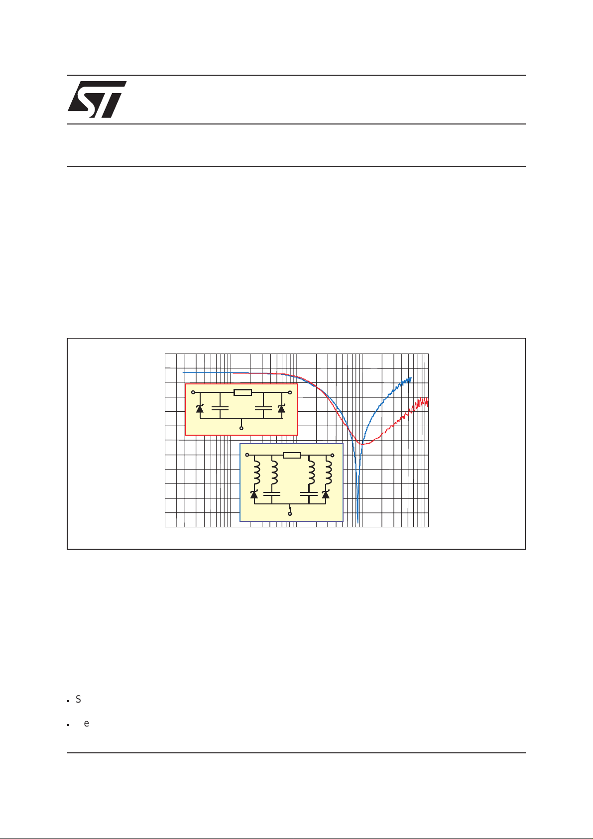
Fig. 1: Frequency response comparison between discrete and IPAD™ filter.
dB
IPADIPAD
DISCRETESDISCRETES
100 MHz10 MHz
1 GHz
Discrete filter will behave like a rejection filter but the rejection frequency will be depending on parasitic inductances while the IPAD filter will act like a low pass filter.
EMIF filters have three main functions, the first is of course to filter EMI/RFI, the second isto protect inputs
and outputs against ESD and the third one is to transmit data from inputs to outputs. EMIF datasheets provide data and curve measured in specific conditions. The goal of this note is to explain test conditions for
EMIF devices.
1-Frequency response
EMIF target is to pass low frequency signals and to reject frequency higher than 800MHz especially
900MHz, 1.8 and 2.4GHz.
Attenuation curve provided in specification shows :
n
Simulation thanks to the Aplac (or P-Spice) tool. This is done before the die design to be sure the device
will fit customer requirements
n
Measurement done on demonstration board.
September 2003 - Ed: 1
1/7
Page 2
AN1751 - APPLICATION NOTE
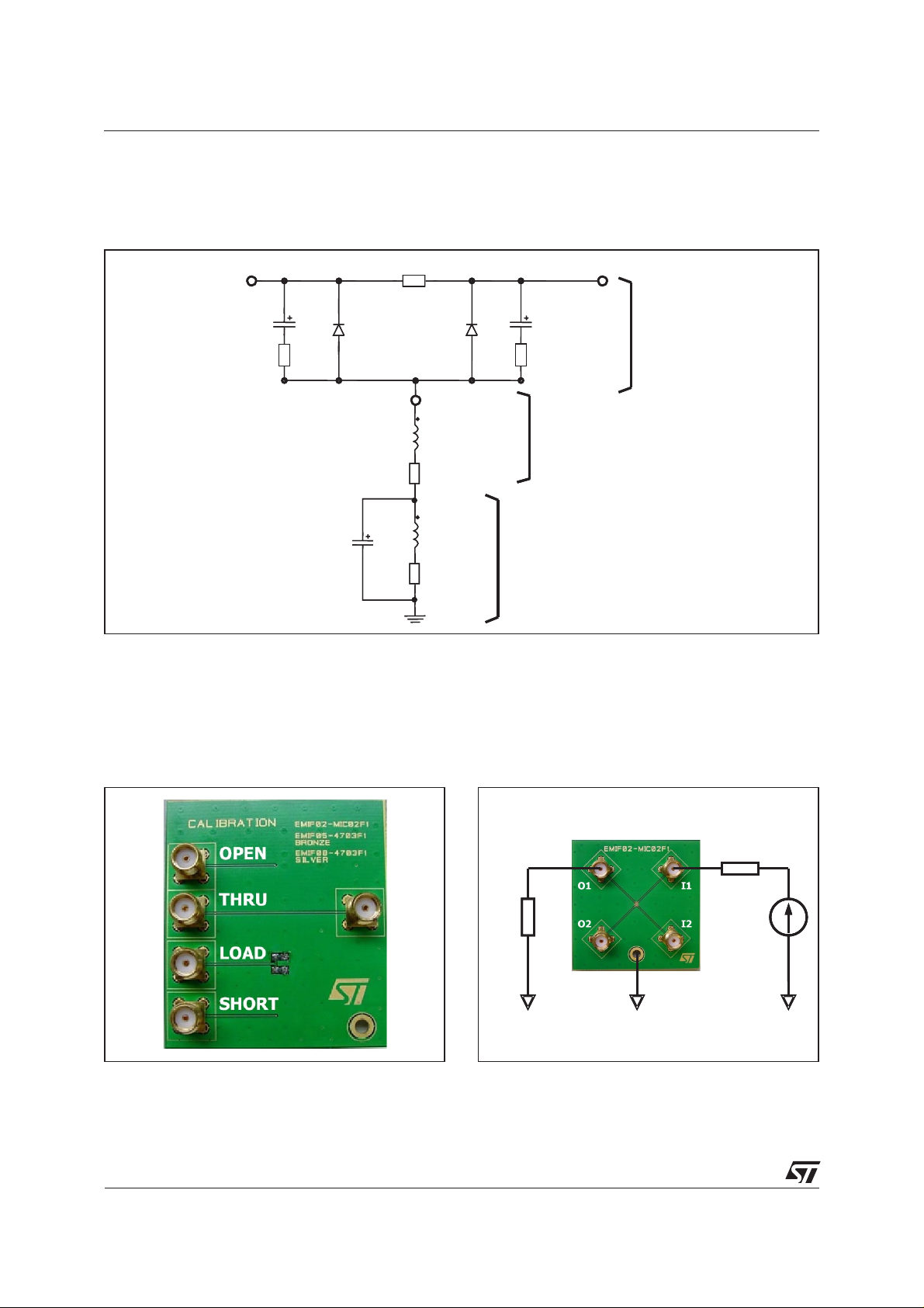
Aplacmodels take into account ofdie, bumps and via for the ground connections. Itdoes not consider PCB
track in the application.
Figure 2
Fig. 2: Aplac model for die, bumps and PCB via.
represents an example of Aplac model for one filtering cell.
I1 O1
Rs
Cin
Rsubump
MODEL = D01
MODEL = D02
Cout
Rsubump
gnd
Die model
Bump model
Via model
Cgnd
Lbump
Rbump
Lgnd
Rgnd
P-Spice is probably the most wellknown simulation software in electronic industry. Limits of P-Spice is
reached when trying to simulate RF signals because of the time it takes for each simulation. It is also
impossible to simulate crosstalk phenomena. Aplac has been developed to avoid all these P-Spice
limitations.
Concerning measurements, the first step is to calibrate the equipment. This is why demoboards are
delivered with a calibration kit shown in
Fig. 3: Calibration board.
figure 3
while the IPAD™ device is on another board (
Fig. 4: Measurement condition on demoboard.
50 Ω
figure 4
).
50 Ω
Vg
If test equipment is not calibrated, non negligible error can occur as the attenuation measurement will
correspond to the one of the IPAD™ + board + connections. Furthermore measurement is done with a
50 Ω load while some applications may have other impedances.
2/7
Page 3
AN1751 - APPLICATION NOTE
2- ESD and latch-up measurements
I/O lines of a cellular phone must be protected against ESD. Most popular ESD standard is the
IEC61000-4-2 having a surge generator defined in
Fig. 5: IEC61000-4-2 generator and the result on a non protected integrated circuit die.
L1 R2 L2
R1
figure 5
.
++
C1
-GND GND
C2
To pin
IEC61000-4-2 specifies C1 charged up to 8kV (contact) and 15kV (air discharge). The MIL-STD 883E
Method 3015.7 is also a reference.
All external pins (bottom connectors, microphone jack…) may be subjected to these kinds of surges. If no
protection is used, result will be the destruction of the internal silicon chip. Destroyed I/O is generally a
short circuit as silicon melt on a very small area as shown in
figure 5
.
IfESD protection device is the minimun to prevent failure, layout is also very important as veryhigh dI/dt of
surge will generate a high LdI/dt.
This means even with a protection device, an integrated circuit can be destroyed because of layout
problem.
Figure 6
explains differences between 2 layouts.
Fig. 6: Two layouts for two very different results.
L6
L2
L1
L6
L1
IC to be
IC to be
IC to be
protected
protected
protected
Wrong layout
V
V
IC
CL
L3
L4L5
V
IN
IC to be
IC to be
IC to be
V
IC
protected
protected
protected
V
CL
V
IN
L2L3
Correct layout
Knowing all PCB tracks are equivalent to an inductance, in the first case the IC will see a voltage:
= (L1+L2+L3+L4) x dI/dt + V
V
IC
CL
With a track lengh, for protection device connection, of 2cm (1cm from side to side), 35µ thickness, 0.5mm
wide (microstrip track) then L2+L3 = 8nH
Considering a 15kV ESD surge surge having dI/dt = 50A/0.7ns
The result is V
= 570V
IC
3/7
Page 4

AN1751 - APPLICATION NOTE
Overvoltage being directly linked to track lengh, voltage across IC may be much higher with few more
centimeters. Most of IC will not like it.
With the correct layout, no high current is flowing through L6 and L3, then V
IC=VCL
In the first case, IC can be destroyed while with the second layout IC is perfectly protected.
Figure7
ESD is applied on input (V
givesinput and output voltages of an EMI filter withthe suitable layout. The demoboard shows the
), while EMIF output (V
IN
) is connected to the IC to be protected.
OUT
Fig. 7: ESD demoboard and measurements on EMIF10-1K010F1.
ESD test board for EMI
Out
Out
Out
Vout measurement Vin measurement
EMI
EMI
EMI
EMI
325
325
325
325
GND
GND
E
E
E
E
In
In
In
Figure 8
shows the equivalent schematic with the ESD surge generator, the EMI Filter and the load which
corresponds to the device to be protected.
Fig. 8: Equivalent schematic of EMI filter connected to ESD surge generators.
R
I/O
RdRd
Vout
V
BR
V
BR
4/7
Vg
VgRdVg
Rg
VinVinVin
R
Load
Page 5

AN1751 - APPLICATION NOTE
Using EMI filter, protection is done in two steps. The first ESD diode will limit the VINvoltage to:
Rg V Rd Vg
×+×
V
=
IN
V
=
OUT
Taking into account of:R>>Rd,Rg>>RdandRload>> Rd (open circuit on the test board).
BR
Rg Rd
+
RV RdV
×+×
BR IN
RRd
+
IO
/
With Vg = 15kV, Rg = 330Ω applied to the EMIF10-1K010F1 board (Rd = 1Ω ,V
= 53V and V
V
IN
With a correct layout, maximum output voltage is closed to V
OUT
= 8.4V
.
BR
= 8V and R
BR
=1kΩ)
I/O
Early ageing and destruction of IC is often due to latch-up phenomena which is mainly induced by dV/dt.
Thanks to its RC structure, EMI filters provide high immunity to latch-up by integration of fast edges.
Measurements done on
figure 7
show very clearly the high efficiency of the structure.
3- Crosstalk measurements
3a - Digital crosstalk
Crosstalk phenomena are due to coupling between 2 lines (2 filters in our case). Coupling factors (β12 and
β21) shown in
figure 9
increase when distance between lines decreases, particularly in silicon dice where
distances between components are very short.
In the example above the expected signal on load RL2 is α2 x Vg2, in fact the actual voltage at this point
has got an extra value β21 x Vg1. This part of the Vg1 signal represents the effect of the crosstalk
phenomenon of the line 1 on the line 2.
This phenomenon has to be taken into account when drivers impose fast digital data or high frequency
analog signals. The disturbed line will be more affected if it works with low voltage signal or high load
impedance (few kΩ).
Fig. 9: Crosstalk phemonema.
Rg1
Line 1
R
Vg1
L1
Rg2
Line 2
R
Vg2
L2
Drivers Receivers
αβ1 x Vg1 + 12 x Vg2
αβ2 x Vg2 + 21 x Vg1
5/7
Page 6

AN1751 - APPLICATION NOTE
For digital crosstalk, test is done thanks to a square pulse generator connected in Vg1 through a 74HC04
gate. An oscilloscope is connected to Vg2.
Figure10
Fig. 10: Digital crosstalk measurement circuit.
showsthe measurement circuit used toquantify crosstalk effectin a classicaldigital application.
½ 74HC04½ 74HC04
Rg1
Line 1
Vg1
+ 5V
Line 2
β21 x Vg1
Figure 11
shows with a signal from 0 to 5V and rise time of few ns, the impact on the disturbed line is less
than 40mV peak to peak: no data disturbance was noted on the concerned line. The measurements
performed with falling edges gives an impact within the same range.
Fig. 11: Digital crosstalk results (EMIF10-1K010F1).
3b - Analog crosstalk
Figure12
givesthe measurement circuit for analogcrosstalk. In
figure13
,the curve shows the effectof cell
on filter I1/O1 on cell I2/O2 for the EMIF10-1K010F1. In usual frequency range of analog signals (up to
100MHz) the effect on disturbed line is less than -47 dB
6/7
Page 7

AN1751 - APPLICATION NOTE
Fig. 12: Analog crosstalk measurement circuit.
Fig. 13: Typical analog crosstalk result
(EMIF10-1K010F1).
50
Ω
Vg
50
Ω
4- Conclusion
EMI filter are designed to suppress EMI and RFI noises and are also used to protect sensitive systems
against electro-static discharges. The use of an Z-R-Z structure provides a very stable voltage on the
output during ESD discharge when layout has been correctly routed.
RF measurement must be done carefully after using calibration board provided with EMIF demoboards.
EMI filters on flipchip are the most efficient topology to filter and protect integrated circuit by saving PCB
area.
Informationfurnishedisbelieved to be accurate and reliable. However, STMicroelectronics assumes no responsibility for the consequences of
useof such information nor for any infringement of patents or other rightsofthird parties which may result from its use. No license isgrantedby
implication or otherwise under any patent or patent rights of STMicroelectronics. Specifications mentioned in this publication are subject to
change without notice. This publication supersedes and replaces all information previously supplied. STMicroelectronics products are not authorized for use as critical components in life support devices or systems without express written approval of STMicroelectronics.
The ST logo is a registered trademark of STMicroelectronics.
All other names are the property of their respective owners.
© 2003 STMicroelectronics - All rights reserved.
STMicroelectronics GROUP OF COMPANIES
Australia - Belgium - Brazil - Canada - China - Czech Republic - Finland - France - Germany -
Hong Kong - India - Israel - Italy - Japan - Malaysia - Malta - Morocco - Singapore - Spain -
Sweden - Switzerland - United Kingdom - United States
www.st.com
7/7
 Loading...