

Page 1
AN1743
APPLICATION NOTE
AUDIO AMPLIFIER SYSTEM USING THE
ANALOG SWITCH STG3699
1. ABSTRACT
This application note is an explanation of the correct use of the STG3699 Analog Switch in mobile
telecom applications.
2. E.S.D. PROTECTION CIRCUITRY DESCRIPTION
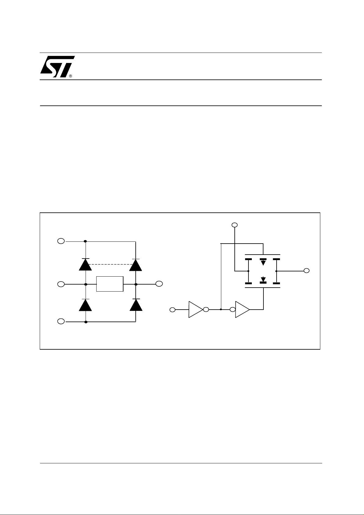
The STG Anal og Switch can be used bi-direc tionally (one input/two outputs or two inputs/one output)
depending on the application. Both inputs and outputs are protected from the E.S.D. discharge by a
circuit that can be synthesized as four protection diodes (two versus V
Figure 1: Generic Circuit for E.S.D. Discharge Protection
Vcc
Input
Output
and two versus GND).
CC
Input
Output
M. Porto
GND
Digital Input IN
To correctly use these devices it is very important to consider the presence of the protection diodes.
For example, a possible problem area is applying a wrong input level signal (input level higher than
power supply). In fact, in this condition the diode versus V
the input to V
The values of the Human Body Model discharge for the STG3699 are very good. In fact the device was
good after a 3KV discharge.
July 2003
, damaging the device or causing incorrect function of the Analog Switch.
CC
is forward biased, so a current will flow from
CC
1/4
Page 2
AN1743 - APPLICATION NOTE
The following tables show the absolute maximum rating characteristics for the STG3699 device and the
correct signal level applicable to these devices to avoid possible problems.
Table 1: Absolute Maximum Rating
Symbol Parameter Value Units
Vcc Supply Voltage -0.5 to +4.6 V
VI DC Input Voltage -0.5 to Vcc +0.5 V
VIC DC C ontrol Input Voltage -0.5 to +4.6 V
VO DC Output Voltage -0.5 to Vcc +0.5 V
Table 2: Ri ght Level Appl icable in Opera ti ng C onditions
Symbol Parameter Value Units
Vcc Supply Voltage 1.65 to 3.6 V
VI DC Input Voltage
VIC DC Control Input Voltage
≤
Vcc V
≤
Vcc V
VO DC Ou tput Voltage 0 to Vcc V
3. APPLICATION
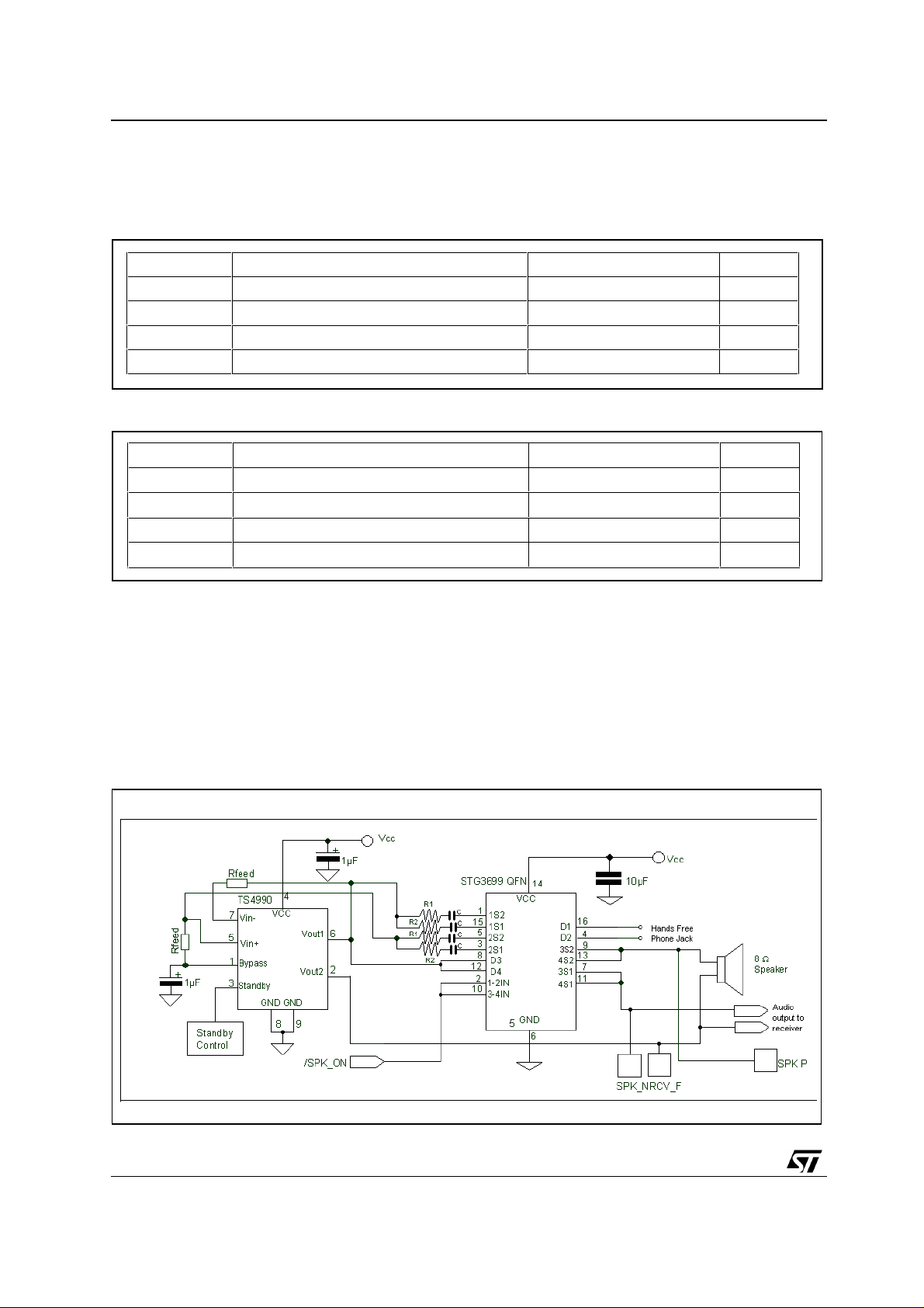
Usually, in telecom mobile application s, an Audio Amplifier drives the Analog Switch. So the designer
must consider different parameters to realize a PCB without problems.
A channel-to-channel Cross Talk or a drift of a few parameters are typical problems of bad coupling
between the Audio Amplifier and the Analog Switch.
The following schematic shows a typical speaker amplifier system for telecom mobile phones.
Figure 2: Audio System Amplifier Schematic
2/4
Page 3

AN1743 - APPLICATION NOTE
For correct power supply stability, it is necessary to apply a capacitance of 10µF to the S TG Analog
Switch and 1µF to the Audio Amplifier between the V
pin signal and GND to filter all possible noise
CC
from the Power Supply voltage.
To use the audio amplifier TS4990 correctly in differential mode, it is important to apply two resistors with
different values as a fun ction of th e gai n and t he righ t power coupling between possible loads applied to
the Analog Switch.
The values of the resistors can be found using the formula 2*Rfeed/R1 or 2*Rfeed/R2.
As the TS4990 does not hav e common mod e feedback, an input-couplin g capacitor before resistors R1
and R2 is mandatory. The capacitor value is calculated by the formula C = 1/2π*R1* FC
or C = 1/2π*R2*FC where FC is the lowest cut off frequency signal required.
Usually the hands fr ee phone jack circuitry presents a c apacitance that when coupled with the analog
switch inputs (D1 or D2 for example) creates cross talk between channel OFF and channel ON.
For instance a 100pF capacitance present on the D1 input generates a noise between channels of
145mV as shown in the following picture.
Figure 3: Noise Present on Analog Switch Channel OFF
V
=3.8V
CC
=3.6V
V
in
In Frequ. =20ΚΗz
Com Load =100pF
Xtalk =27.80dB
Using the formula : XTALK (dB) = 20log Vout /Vin, it is pos sible t o ge t back to the cross talk val ue. I f this
value is low a possible signal interference can induce noise between two different loads applied to the
outputs of the Analog Switch, therefore causing the system to function badly.
4. CONCLUSION
These pages describe possible problems applying the STG3699 Analog Switch when the operating
conditions stated in the specifications are not adhered to, resulting in less than the guaranteed
functionality for these devices being achieved.
3/4
Page 4

AN1743 - APPLICATION NOTE
Information furnished is believed to b e accurate an d reliable. How ever , STM icroelectronics assum es no resp onsibility
for the consequences of use of such information nor for any infringement of patents or other rights of third parties
which may result from its use. No license is granted by implication or otherwise under any patent or patent rights of
STMicroelectronics. Specification ment ioned in this p ublication are subject to change without notice. This pub lication
supersedes and repla ces all information previou sly supp lied. STM icro elect ronics pro ducts are not authorized for use
as critical components in life support devices or systems witho ut expres s written approva l of STMicroelect ro nics.
The ST logo is a registered trademark of STMicroelectronics
© 2003 STMicroelectronics - Printed in Italy - All rights reserved
Australia - Brazil - Canada - China - Finland - France - Germ any - Hong Kon g - India - Isreal - Italy - Japan - Malaysia
- Malta - Morocco - Singapore - Spain - Sweden - Switzerland - United Kingdom - U.S.A.
4/4
STMicroelectronics GROUP OF COMPANIES
http://www.st.com
 Loading...