

Page 1
AN1736
Application note
VIPower: VIPer22A dual output reference
board 90 to 264 VAC input, 10W output
Introduction
This is an off-line wide range VIPer22A dual outputs power supply at a switching frequency
of 60kHz and is set up for secondary regulation with an optocoupler. One output delivers 5V
at 1A and while a second output delivers12V at 0.42A, making up the total output power of
10W.
● Switch mode general purpose power supply
● Single-sided board
● 75% efficiency
● Output short circuit protection
● Thermal shutdown protection
● Meets EN55022 class B EMI specification
● Meets Blue Angel
Operating conditions
Parameter Limits
Input voltage range 90 to 264Vac
Input Frequency Range 50/60 Hz
Output voltages V1= 5V; V2=12V
Output current I=0.84A
Output power 10W
Efficiency 75% typical
Line regulation +/- 0% for 5V output
Load regulation +/- 0.3% for 5V output
Output ripple voltage 20mVpp
EMI EN55022 Class B
July 2006 Rev 4 1/20
www.st.com
Page 2

Contents AN1736
Contents
1 PCB lay-out . . . . . . . . . . . . . . . . . . . . . . . . . . . . . . . . . . . . . . . . . . . . . . . . 5
2 Line regulation . . . . . . . . . . . . . . . . . . . . . . . . . . . . . . . . . . . . . . . . . . . . . . 6
3 Load regulation . . . . . . . . . . . . . . . . . . . . . . . . . . . . . . . . . . . . . . . . . . . . . 7
4 Efficiency . . . . . . . . . . . . . . . . . . . . . . . . . . . . . . . . . . . . . . . . . . . . . . . . . . 8
5 Line frequency ripple . . . . . . . . . . . . . . . . . . . . . . . . . . . . . . . . . . . . . . . . 9
6 Switching frequency ripple . . . . . . . . . . . . . . . . . . . . . . . . . . . . . . . . . . 10
7 Transient load response . . . . . . . . . . . . . . . . . . . . . . . . . . . . . . . . . . . . . 11
8 EMI results . . . . . . . . . . . . . . . . . . . . . . . . . . . . . . . . . . . . . . . . . . . . . . . . 12
9 Blue Angel . . . . . . . . . . . . . . . . . . . . . . . . . . . . . . . . . . . . . . . . . . . . . . . . 13
9.1 Stand-by input power . . . . . . . . . . . . . . . . . . . . . . . . . . . . . . . . . . . . . . . . 13
10 Transformer specification . . . . . . . . . . . . . . . . . . . . . . . . . . . . . . . . . . . 14
11 Output current and voltage capability . . . . . . . . . . . . . . . . . . . . . . . . . . 15
12 Thermal considerations . . . . . . . . . . . . . . . . . . . . . . . . . . . . . . . . . . . . . 16
13 Component list . . . . . . . . . . . . . . . . . . . . . . . . . . . . . . . . . . . . . . . . . . . . 17
14 Revision history . . . . . . . . . . . . . . . . . . . . . . . . . . . . . . . . . . . . . . . . . . . 19
2/20
Page 3

AN1736 List of figures
List of figures
Figure 1. Board lay-out . . . . . . . . . . . . . . . . . . . . . . . . . . . . . . . . . . . . . . . . . . . . . . . . . . . . . . . . . . . . 5
Figure 2. Board top legend (not in scale). . . . . . . . . . . . . . . . . . . . . . . . . . . . . . . . . . . . . . . . . . . . . . . 5
Figure 3. Board bottom foil (not in scale) . . . . . . . . . . . . . . . . . . . . . . . . . . . . . . . . . . . . . . . . . . . . . . . 5
Figure 4. Line regulation . . . . . . . . . . . . . . . . . . . . . . . . . . . . . . . . . . . . . . . . . . . . . . . . . . . . . . . . . . . 6
Figure 5. Load regulation for 5V output . . . . . . . . . . . . . . . . . . . . . . . . . . . . . . . . . . . . . . . . . . . . . . . . 7
Figure 6. Load regulation for 12V output . . . . . . . . . . . . . . . . . . . . . . . . . . . . . . . . . . . . . . . . . . . . . . . 7
Figure 7. Efficiency vs. input voltage . . . . . . . . . . . . . . . . . . . . . . . . . . . . . . . . . . . . . . . . . . . . . . . . . . 8
Figure 8. Efficiency vs. Pout . . . . . . . . . . . . . . . . . . . . . . . . . . . . . . . . . . . . . . . . . . . . . . . . . . . . . . . . 8
Figure 9. Line ripple for 5V output . . . . . . . . . . . . . . . . . . . . . . . . . . . . . . . . . . . . . . . . . . . . . . . . . . . . 9
Figure 10. Line ripple for 12V output . . . . . . . . . . . . . . . . . . . . . . . . . . . . . . . . . . . . . . . . . . . . . . . . . . . 9
Figure 11. Switching ripple for 5V output . . . . . . . . . . . . . . . . . . . . . . . . . . . . . . . . . . . . . . . . . . . . . . . 10
Figure 12. Switching ripple for 12V output . . . . . . . . . . . . . . . . . . . . . . . . . . . . . . . . . . . . . . . . . . . . . . 10
Figure 13. Transient load response . . . . . . . . . . . . . . . . . . . . . . . . . . . . . . . . . . . . . . . . . . . . . . . . . . . 11
Figure 14. EMI . . . . . . . . . . . . . . . . . . . . . . . . . . . . . . . . . . . . . . . . . . . . . . . . . . . . . . . . . . . . . . . . . . 12
Figure 15. Mechanical drawings of the transformer . . . . . . . . . . . . . . . . . . . . . . . . . . . . . . . . . . . . . . . 14
Figure 16. Schematic diagram . . . . . . . . . . . . . . . . . . . . . . . . . . . . . . . . . . . . . . . . . . . . . . . . . . . . . . . 18
3/20
Page 4

List of tables AN1736
List of tables
Table 1. Input power in no load condition at different input voltage . . . . . . . . . . . . . . . . . . . . . . . . . 13
Table 2. Change in output voltage and current. . . . . . . . . . . . . . . . . . . . . . . . . . . . . . . . . . . . . . . . . 15
Table 3. Bill of material . . . . . . . . . . . . . . . . . . . . . . . . . . . . . . . . . . . . . . . . . . . . . . . . . . . . . . . . . . . 17
Table 4. Revision history . . . . . . . . . . . . . . . . . . . . . . . . . . . . . . . . . . . . . . . . . . . . . . . . . . . . . . . . . 19
4/20
Page 5
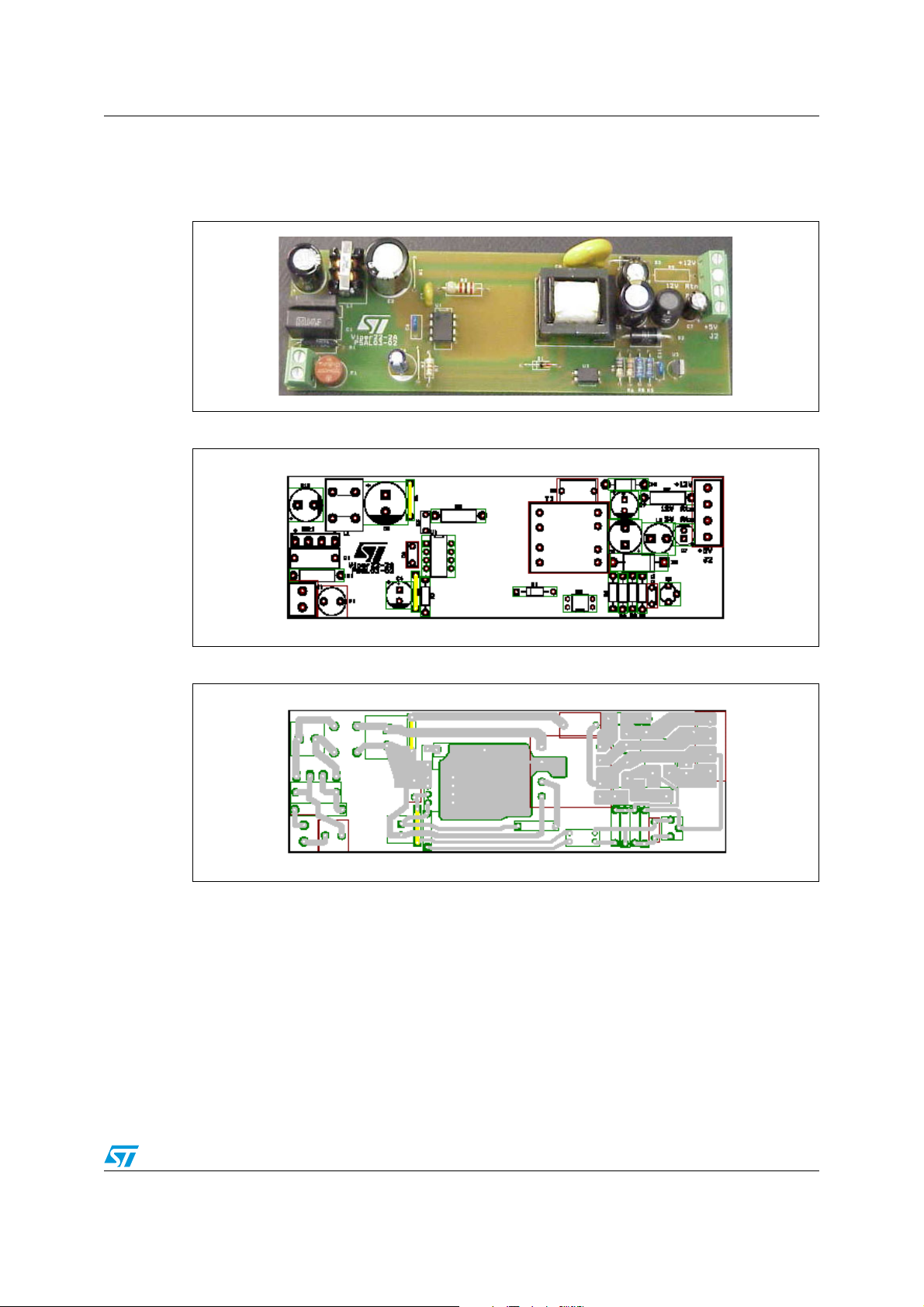
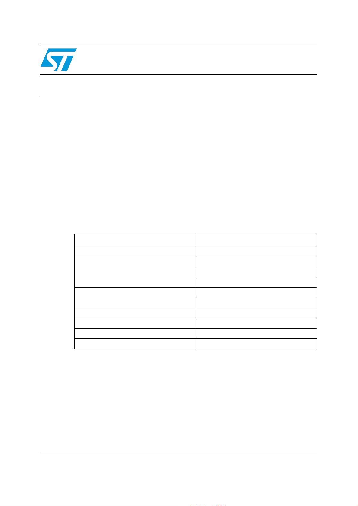
AN1736 PCB lay-out
1 PCB lay-out
Figure 1. Board lay-out
Figure 2. Board top legend (not in scale)
Figure 3. Board bottom foil (not in scale)
5/20
Page 6
Line regulation AN1736
2 Line regulation
Figure 4. shows the line regulation of both the +5V and the +12V output. The output
voltages are measured for the input voltage range of 85 to 264VAC at the maximum output
power of 10W. The +5V output shows a 0% line regulation while the +12V output has a line
regulation of 0.25%.
Figure 4. Line regulation
14
12
10
8
6
4
Output Voltage (Vdc)
2
50 100 150 200 250 300
Input Voltage (Vac)
5V
12V
6/20
Page 7

AN1736 Load regulation
3 Load regulation
The load regulation measurements are taken at the input voltage of 120Vac. Here, the load
regulation measured for the +5V output is ±0.3% while the +12V output shows a load
regulation of ±0.46%. See Figure 5. and Figure 6.
Figure 5. Load regulation for 5V output
5.5
5.25
5
4.75
4.5
4.25
Output Voltage (V)
4
0 0.2 0.4 0.6 0.8 1 1.2
Output Current (A)
V1
Figure 6. Load regulation for 12V output
12.5
12.4
12.3
12.2
12.1
12
11.9
11.8
Ouput Voltage (V)
11.7
11.6
11.5
0 0.1 0.2 0.3 0.4
Output Current (A)
V2
7/20
Page 8

Efficiency AN1736
4 Efficiency
Figure 7. shows the efficiency curve of the reference board when the input voltage is varied
from 90 to 264Vac at the maximum output power of 10W. Here, the typical efficiency value
is measured to be 75%.
Meanwhile, Figure 8. shows the efficiency measurement taken at 120Vac while the output
power is varied from 1W to the maximum 10W. The typical efficiency measured is also
around 75%.
Figure 7. Efficiency vs. input voltage
83.00%
82.00%
81.00%
80.00%
79.00%
78.00%
77.00%
76.00%
Efficiency (%)
75.00%
74.00%
73.00%
72.00%
50 100 150 200 250 300
Vin (Vac)
Efficiency
Figure 8. Efficiency vs. Pout
85.00%
80.00%
75.00%
70.00%
65.00%
60.00%
55.00%
Efficiency (%)
50.00%
45.00%
40.00%
0.00 5.00 10.00 15.00
Efficiency
Pout (W)
8/20
Page 9

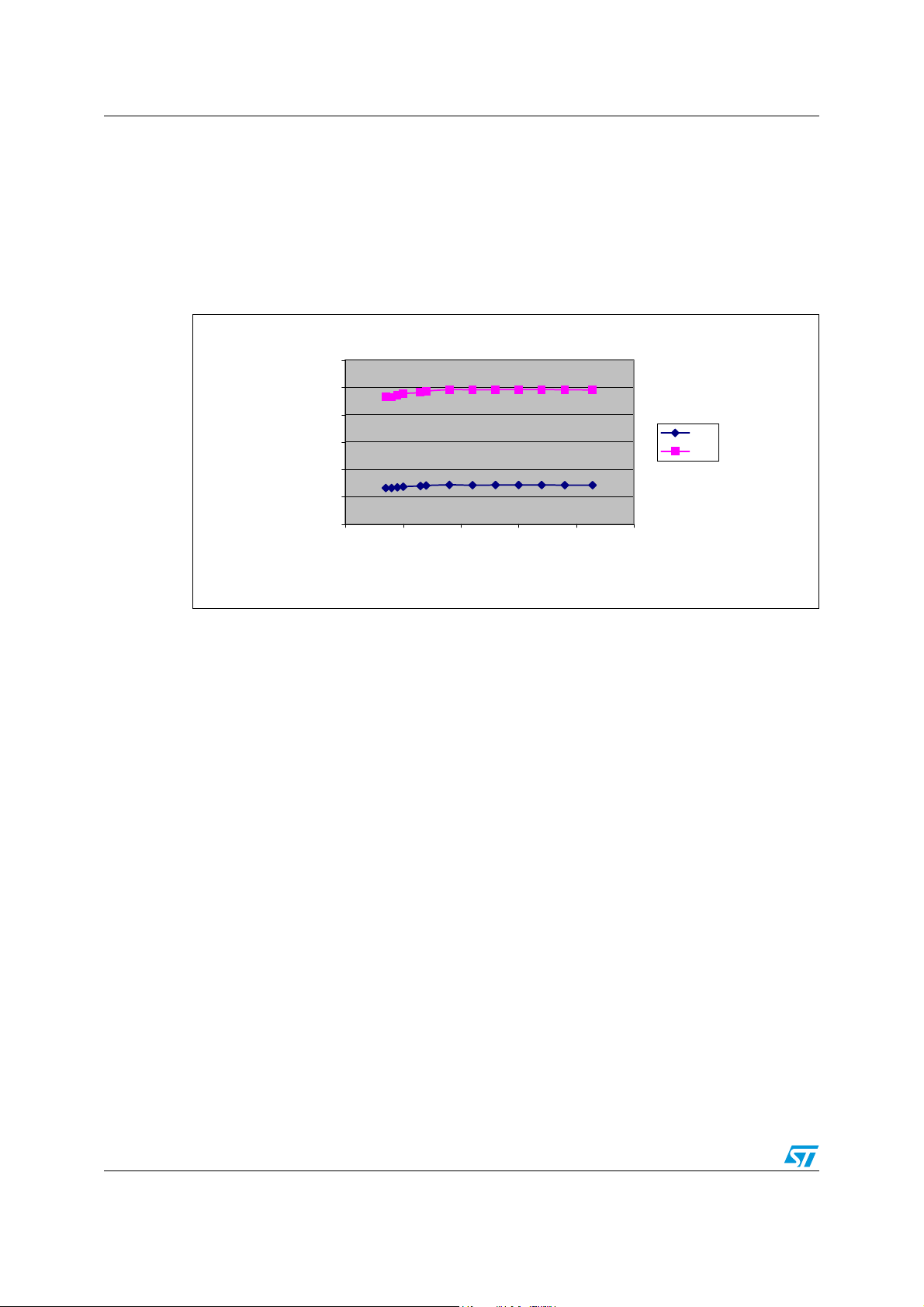
AN1736 Line frequency ripple
5 Line frequency ripple
Figure 9. Line ripple for 5V output Figure 10. Line ripple for 12V output
Figure 9. and Figure 10. show the line frequency ripple waveforms of the +5V and +12V
output respectively taken at 90Vac input. The line frequency ripple for +5V is 10mVpp while
for the +12V output; it is 50mVpp.
9/20
Page 10
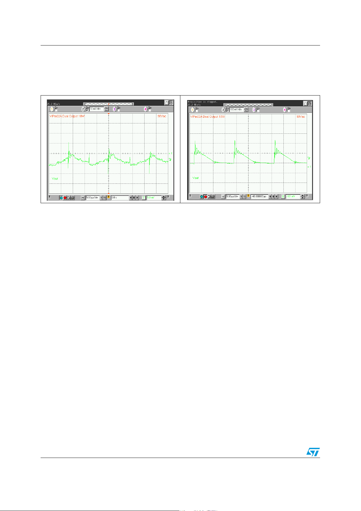
Switching frequency ripple AN1736
6 Switching frequency ripple
Figure 11. Switching ripple for 5V output Figure 12. Switching ripple for 12V output
The switching ripple for the +5V output measured is 12mVpp while this ripple measured for
the +12V output is 200mVpp. The low ripple for the +5V output is obtained using the low
pass LC (PI) filter configuration of L2 and C10. The waveforms are taken at the input voltage
of 90Vac.
10/20
Page 11

AN1736 Transient load response
7 Transient load response
Figure 13. Transient load response
The transient load response is measured at the input voltage of 90Vac where the +5V output
load is varied from 50% load (0.5A) to 100% load (1A) while the +12V is kept at the nominal
load value of 0.21A. The dynamic response measured is 140mV or 2.8% while the settling
time is 500ms. See Figure 13.
11/20
Page 12

EMI results AN1736
8 EMI results
Figure 14. EMI
The unit passes the European Norm, EN55022 Class B EMI.
12/20
Page 13

AN1736 Blue Angel
9 Blue Angel
The reference board meets the Blue Angel Norm, consuming less than 1W total when
working in stand-by mode. The board operates in burst mode when both the output loads
are reduced to zero and the output voltages still remain regulated.
9.1 Stand-by input power
Table 1. Input power in no load condition at different input voltage
Input Voltage Input Wattage at No Load
115Vac 210.38mW
230Vac 331.85mW
At the input voltage of 120Vac, a minimum load of 100mA is needed to keep the total input
power consumption to be less than 1W.
13/20
Page 14

Transformer specification AN1736
10 Transformer specification
Figure 15. Mechanical drawings of the transformer
Meets Construction
for:
UL 1310, 1950,1411,
IEC 61558-1,2-17,
EN60950
www.cramercoil.com
When the VIPer22A (U1) is on, energy is stored in the primary winding of transformer (1-2),
TX1. This energy is transferred to the auxiliary winding (3-4), and to the output (5-6) when
the VIPer22A is off. The auxiliary winding provides the bias voltage for the VIPer22A at pin 4
(Vdd).
The electrical specifications of the transformer are as follow
● Primary Inductance 2.25mH±15%
● Primary Leakage Inductance 22µH typical
● Turns Ratio (N1/N5:N2) 1:0.053
● Turns Ratio (N1/N5:N3) 1:0.127
● Turns Ratio (N1/N5:N4) 1:0.167
:
The transformer is designed and manufactured by Cramer Coil and Transformer.
14/20
Page 15

AN1736 Output current and voltage capability
11 Output current and voltage capability
The standard voltage and current values for the reference board can be changed to deliver a
different voltage and current value, with changes to the following components as detailed in
Table 2.
Table 2. Change in output voltage and current
Output Voltages T1 C9
5 and 12V CVP32-002 220
5 and 15V CVP32-003 220
5 and 24V CVP32-004 220
µF/25V
µF/35V
µF/50V
15/20
Page 16

Thermal considerations AN1736
12 Thermal considerations
The reference board is single-sided and utilizes a wide area of two ounces copper pad to act
as a heat sink for the VIPer22ADIP. All other traces utilize one-ounce copper.
16/20
Page 17

AN1736 Component list
13 Component list
Table 3. Bill of material
Quantity Reference Description
1 BR1 KBP210GDI
1 C1 0.047µF/250V boxcap
1C2 22µF/400V electrolytic
1 C3 100pF 1kV ceramic
1C4 22µF/25V electrolytic
1C5 680µF/25V electrolytic
1 C6 22nF/50V ceramic
1C7 100µF/25V electrolytic
1 C8 4.7nF/250V Y cap
1C9 210µF/25V electrolytic
1 C11 0.01µF/50V ceramic
1 C12 10µF/400V electrolytic
1 D1 1N4148
1 D2 1N5821
1 D3 STMicroelectronics BYW100-200
1 F1 0.5A 250V Fuse
2 J1, J2 Connectors
1 L1 Compostar 2x30mH common-mode line choke
1 L2 Coilcraft 10µH inductor
1R1 5Ω 5% 1W Wire wound
1R2 2KΩ 5% 1/2W
1R4 68Ω 5% 1/4W
1R5 2.438KΩ 1% 1/4W
1 R6 470Ω 5% 1/4W
1R7 9.1kΩ 5% 1/4W
1 R8 2.49KΩ 1% 1/4W
1R9 15KΩ 5% 1/2W
1 T1 Cramer coil transformer CVP32-002
1 U1 STMicroelectronics VIPer22ADIP
1 U2 H11A817A or LTV817 optocoupler
1 U3 STMicroelectronics TL431
2 W1, W2 Jumper wire
17/20
Page 18

Component list AN1736
Figure 16. Schematic diagram
123
4
J2
CON4
C
5V GND
25V
C7
100uF
5 V @ 1.0A
L2
10uH
C5
680uF
25V
D2
1N5821
5
6
.
.
T1
CVP32-002
.
1
R22k0.5W
C3
100pF
L1
30mH
12V Rtn
12V @ 0.42A
R9
0.5W
15k
C9
220uF
25V
D3
BYW100-200
7
.8.
C8
4.7nF
Y1 cap
W1
0
.3.
.
4
2
1kV
0
R7
9.1k
D1
4
1N4148
Vdd
Drain8Drain6Drain7Drain5Source1Source
0
C2
400V
22uF
C12
10uF
400V
2 X 30mH
1%
R8
2.49k
C11
0.01uF
R6
470
U2
R4
68
12
43
3
Fb
U1
VIPe r2 2 A
2
C4
22uF
25V
50V
1%
R5
2.43k
H11A817A
U3
TL43 1
ST
C6
50V
22nF
0
STMicroelectronics
of
11Tuesday, August 30, 2005
VIPer22A Dual Outputs Ref erence Desi gn
1375 East Woodfield Road, Suite 400
Schaumbu rg, IL 60173
B
Title
Size Docume nt Num ber Rev
Date: Sheet
BR1
KBP2 10G DI
2 1
4 3
F1
FUSE
0.5A 5X20mm
250V
C1
0.047uF
1W
R1
5 ohms
L
1
2
J1
N
CON2
85 to 264Vac
All resistors are 1/4 W 5% unless specified.
All capacitors are in uF a nd 50 V unless
specified.
18/20
Page 19

AN1736 Revision history
14 Revision history
Table 4. Revision history
Date Revision Changes
16-Jul-2003 1 First issue
13-Jun-2005 2
09-Sep-2005 3 Schematic modified
31-Jul-2006 4
- Schematic changed
- Component list table modified
- New template
- Component list value modified
19/20
Page 20

AN1736
Please Read Carefully:
Information in this document is provided solely in connection with ST products. STMicroelectronics NV and its subsidiaries (“ST”) reserve the
right to make changes, corrections, modifications or improvements, to this document, and the products and services described herein at any
time, without notice.
All ST products are sold pursuant to ST’s terms and conditions of sale.
Purchasers are solely responsible for the choice, selection and use of the ST products and services described herein, and ST assumes no
liability whatsoever relating to the choice, selection or use of the ST products and services described herein.
No license, express or implied, by estoppel or otherwise, to any intellectual property rights is granted under this document. If any part of this
document refers to any third party products or services it shall not be deemed a license grant by ST for the use of such third party products
or services, or any intellectual property contained therein or considered as a warranty covering the use in any manner whatsoever of such
third party products or services or any intellectual property contained therein.
UNLESS OTHERWISE SET FORTH IN ST’S TERMS AND CONDITIONS OF SALE ST DISCLAIMS ANY EXPRESS OR IMPLIED
WARRANTY WITH RESPECT TO THE USE AND/OR SALE OF ST PRODUCTS INCLUDING WITHOUT LIMITATION IMPLIED
WARRANTIES OF MERCHANTABILITY, FITNESS FOR A PARTICULAR PURPOSE (AND THEIR EQUIVALENTS UNDER THE LAWS
OF ANY JURISDICTION), OR INFRINGEMENT OF ANY PATENT, COPYRIGHT OR OTHER INTELLECTUAL PROPERTY RIGHT.
UNLESS EXPRESSLY APPROVED IN WRITING BY AN AUTHORIZED ST REPRESENTATIVE, ST PRODUCTS ARE NOT
RECOMMENDED, AUTHORIZED OR WARRANTED FOR USE IN MILITARY, AIR CRAFT, SPACE, LIFE SAVING, OR LIFE SUSTAINING
APPLICATIONS, NOR IN PRODUCTS OR SYSTEMS WHERE FAILURE OR MALFUNCTION MAY RESULT IN PERSONAL INJURY,
DEATH, OR SEVERE PROPERTY OR ENVIRONMENTAL DAMAGE. ST PRODUCTS WHICH ARE NOT SPECIFIED AS "AUTOMOTIVE
GRADE" MAY ONLY BE USED IN AUTOMOTIVE APPLICATIONS AT USER’S OWN RISK.
Resale of ST products with provisions different from the statements and/or technical features set forth in this document shall immediately void
any warranty granted by ST for the ST product or service described herein and shall not create or extend in any manner whatsoever, any
liability of ST.
ST and the ST logo are trademarks or registered trademarks of ST in various countries.
Information in this document supersedes and replaces all information previously supplied.
The ST logo is a registered trademark of STMicroelectronics. All other names are the property of their respective owners.
© 2006 STMicroelectronics - All rights reserved
STMicroelectronics group of companies
Australia - Belgium - Brazil - Canada - China - Czech Republic - Finland - France - Germany - Hong Kong - India - Israel - Italy - Japan -
Malaysia - Malta - Morocco - Singapore - Spain - Sweden - Switzerland - United Kingdom - United States of America
www.st.com
20/20
 Loading...