

Page 1

AN1735
Application note
VIPer22A Single Output Reference Board
90 to 264 VAC input, 10W output
Introduction
This Application Note deals with an off-line wide range single output power supply using a
VIPer22A off-line SMPS primary switcher manufactured by STMicroelectronics. The
VIPer22A combines a dedicated current mode PWM controller with a high voltage Power
MOSFET on the same silicon chip and its switching frequency is internally fixed at 60 kHz.
The feedback path of the power supply includes an optocoupler for secondary regulation
and galvanic isolation between primary and secondary sides. The output voltage is
regulated at 12V with a maximum output current of 0.84A, resulting in a maximum output
power of 10W.
Product highlights
– Switch mode General Purpose Power Supply
– Single-sided Board
– 75% Typical Efficiency
– Output Short Circuit Protection
– Thermal Shutdown Protection
– Complies with EN55022 Class B EMI specifications
– Complies with Blue Angel standards
July 2006 Rev 2 1/15
www.st.com
Page 2

Contents AN1735
Contents
1 Summary description . . . . . . . . . . . . . . . . . . . . . . . . . . . . . . . . . . . . . . . . 3
1.1 Board layout . . . . . . . . . . . . . . . . . . . . . . . . . . . . . . . . . . . . . . . . . . . . . . . . 4
2 Test results . . . . . . . . . . . . . . . . . . . . . . . . . . . . . . . . . . . . . . . . . . . . . . . . 5
2.1 Frequency ripple . . . . . . . . . . . . . . . . . . . . . . . . . . . . . . . . . . . . . . . . . . . . . 5
2.2 Efficiency results . . . . . . . . . . . . . . . . . . . . . . . . . . . . . . . . . . . . . . . . . . . . 6
2.3 Load response . . . . . . . . . . . . . . . . . . . . . . . . . . . . . . . . . . . . . . . . . . . . . . 6
2.4 Line and load regulation . . . . . . . . . . . . . . . . . . . . . . . . . . . . . . . . . . . . . . . 7
2.5 EMI emissions . . . . . . . . . . . . . . . . . . . . . . . . . . . . . . . . . . . . . . . . . . . . . . 8
3 Waveforms . . . . . . . . . . . . . . . . . . . . . . . . . . . . . . . . . . . . . . . . . . . . . . . . . 9
4 Output current and voltage capability . . . . . . . . . . . . . . . . . . . . . . . . . . . 9
5 Thermal considerations . . . . . . . . . . . . . . . . . . . . . . . . . . . . . . . . . . . . . 10
6 Blue angel standard . . . . . . . . . . . . . . . . . . . . . . . . . . . . . . . . . . . . . . . . 10
7 Transformer specifications . . . . . . . . . . . . . . . . . . . . . . . . . . . . . . . . . . 11
8 Component list . . . . . . . . . . . . . . . . . . . . . . . . . . . . . . . . . . . . . . . . . . . . 12
9 Revision history . . . . . . . . . . . . . . . . . . . . . . . . . . . . . . . . . . . . . . . . . . . 14
2/15
Page 3
AN1735 Summary description
1 Summary description
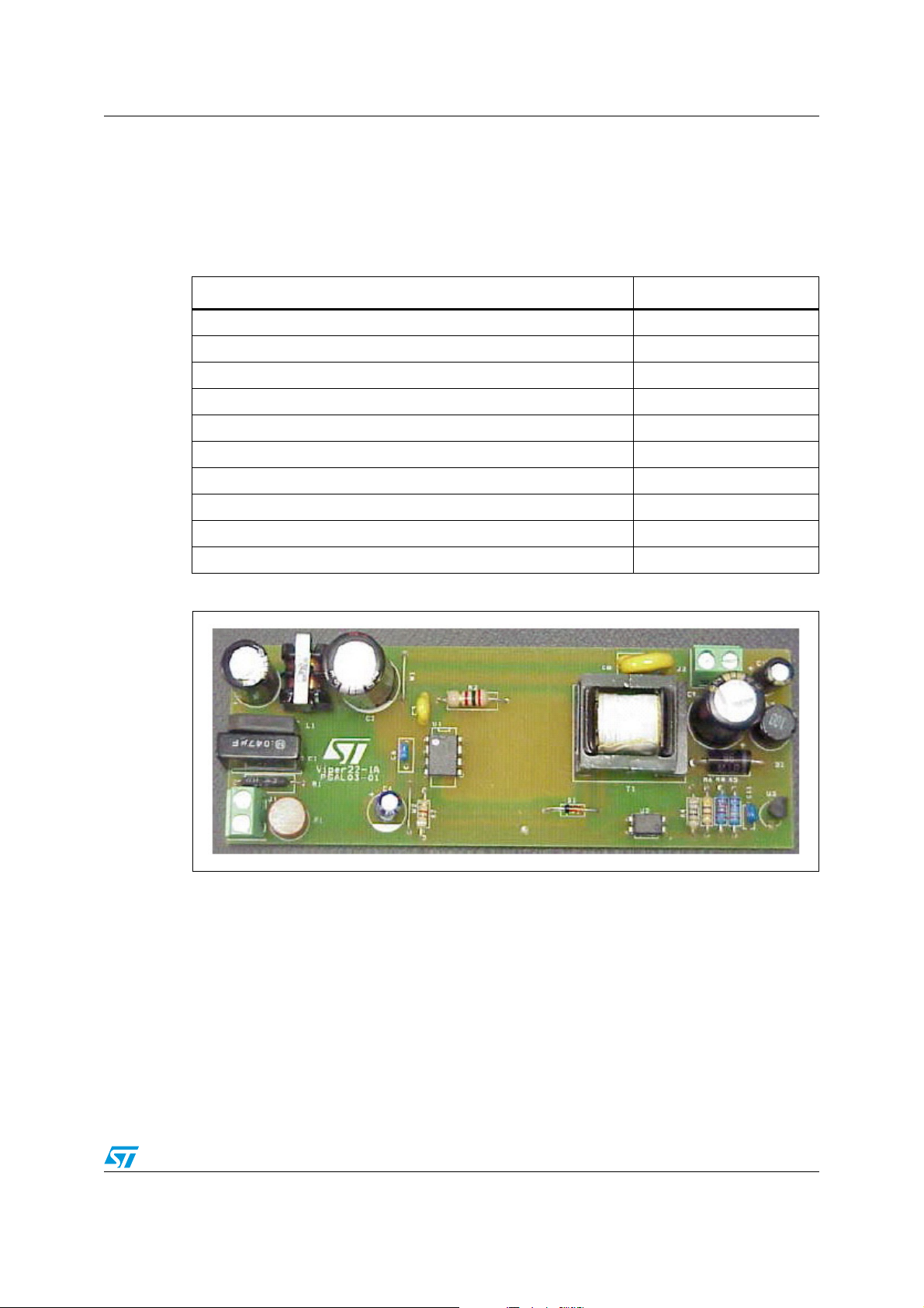
Tab le 1 lists the main parameters of the converter while a prototype of the board is shown in
Figure 1.
Table 1. Operating conditions
Parameter Limits
Input voltage range 90 to 264 V
Input frequency range 50/60 Hz
Output Voltage V=12V
Output current I=0.84A
Output power 10W
Efficiency 75% typical
Line regulation ± 0%
Load regulation ± 0.2%
Output voltage ripple 20m V
EMI EN55022 class B
AC
PP
Figure 1. Board prototype
3/15
Page 4
Summary description AN1735
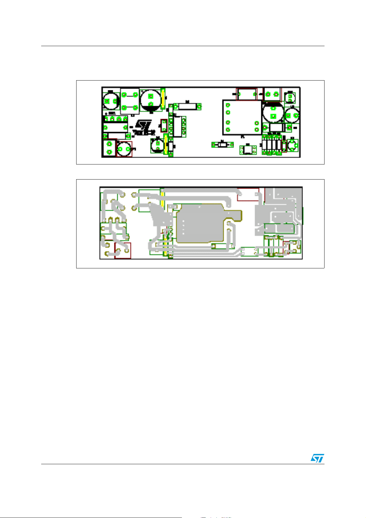
1.1 Board layout
Figure 2. Board top legend (not to scale)
Figure 3. Board bottom foil (not to scale)
4/15
Page 5
AN1735 Test results
2 Test results
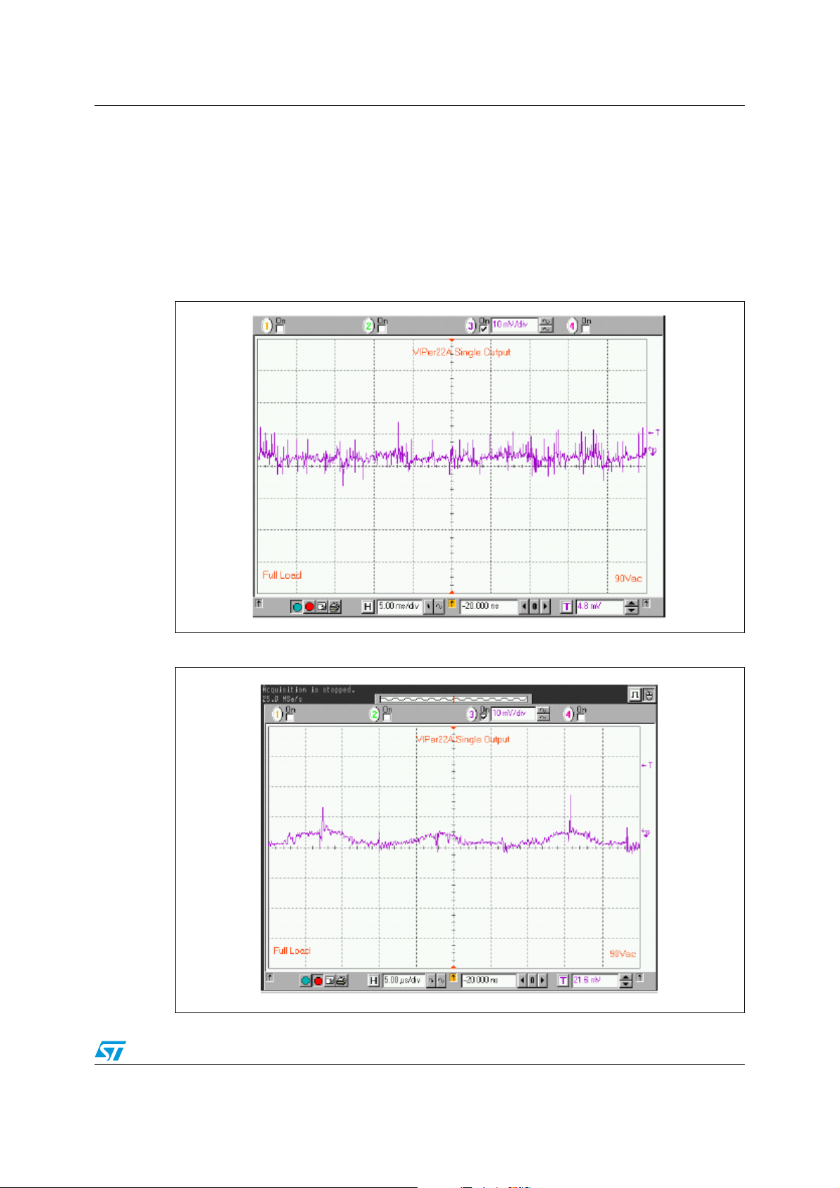
2.1 Frequency ripple
Figure 4 presents the line frequency ripple taken with an input voltage of 90 VAC. A 10mVPP
amplitude is measured at the output. Figure 5 shows the switching ripple on the output at
the full load of 0.84A.
Figure 4. Line frequency ripple
Figure 5. Switching frequency ripple
5/15
Page 6
Test results AN1735
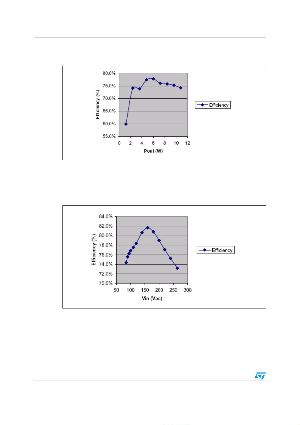
2.2 Efficiency results
Figure 6. Efficiency vs. P
OUT
The typical efficiency of the board is about 75%. The efficiency measurements are taken at
a nominal input voltage of 120 V
. Figure 6 shows the efficiency measurements that are
AC
taken when the output power is varied from 1W to 10W. Figure 7 meanwhile shows the
efficiency measurement taken when the input voltage is varied from 90 to 264 V
at the
AC
maximum output power rating of 10W. The average measured efficiency is 75%.
Figure 7. Efficiency vs. V
IN
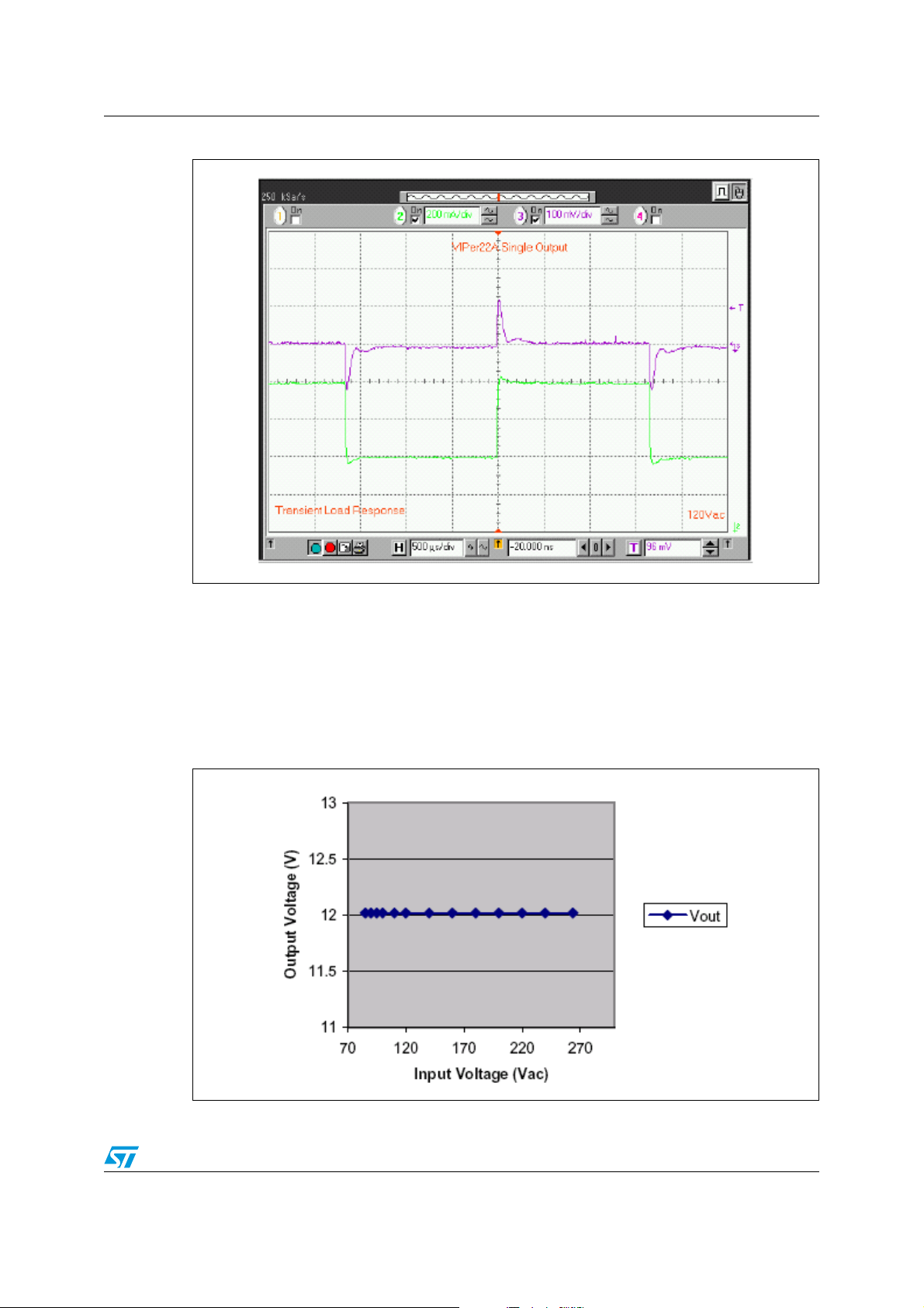
2.3 Load response
At an input voltage of 120 VAC, the output load is stepped from 50% to 100% load (0.42A to
0.84A). The settling time is found to be 400µs and the dynamic regulation is 120mV or 1%.
The resulting waveforms are shown in Figure 8.
6/15
Page 7
AN1735 Test results
Figure 8. Transient load response
2.4 Line and load regulation
The output voltages are measured over the entire input voltage range, that is between 90
and 264 V
graph, the output voltage remained at a constant +12V output. The line regulation therefore
is 0%.
Figure 9. Line regulation
. This gives the line regulation as shown in Figure 9. As can be seen from the
AC
7/15
Page 8

Test results AN1735
The output voltage has also been measured in a range of loads, as shown in Figure 10 at a
nominal input voltage of 120 V
from 10% to 100% of full load on the output.
Figure 10. Load regulation
. The load regulation is approximately 0.125% when tested
AC
2.5 EMI emissions
Figure 11. EMI conducted emissions
The results shown in Figure 11 indicate that the unit passes EN55022 Class B EMI
conducted emission tests.
8/15
Page 9

AN1735 Waveforms
3 Waveforms
Figure 12 shows the drain current (I
)and drain voltage (VDS) during normal operation
DRAIN
at full load. The converter works in the Discontinuous mode as illustrated by the waveforms.
Figure 12. V
and drain current
DS
4 Output current and voltage capability
The output voltage and current can be set to a different value by changing components as
shown in Tab l e 2.
Table 2. Changes in output voltage and current
V
out
5.0V 2.0A CVP32-006 2.49KΩ 1% 2.49KΩ 1% 2x1000µF/25V 100µF/25V
12V 0.84A CVP32-001 13.3KΩ 1% 3.48KΩ 1% 1000µF/25V 100µF/25V
15V 0.67A CVP32-005 14.7KΩ 1% 2.94KΩ 1% 680µF/35V 100µF/35V
24V 0.42A CVP32-007 13.0KΩ 1% 1.50KΩ 1% 220µF/50V 100µF/50V
T1 R8 R5 C9 C10
9/15
Page 10

Thermal considerations AN1735
5 Thermal considerations
The VIPer22A is a single-sided reference board that uses a wide two-ounce copper pad
area to act as a heat sink for the VIPer22ADIP. All other traces use one-ounce copper.
At 65° C, the measured case temperature is 90° C, therefore making the junction
temperature 123.7° C.
6 Blue angel standard
The Blue Angel standard is a German certification for products and services that have
environmentally friendly aspects. It requires that the power supply consumes less than 1W
of power when in Standby mode.
The total power consumption of this reference board is less than 1W when working in
Standby Burst mode. Ta b le 3 lists the input power consumption (P
input voltages when measured with zero loads at the output.
Table 3. Input power consumption in No-Load conditions
) values at different
IN
Input voltage Input Wattage at No Load
115 V
230 V
AC
AC
200 mW
366 mW
In order to keep the total input power to be less than 1W total, a minimum load of 40 mA is
needed when using a 120 V
input supply.
AC
Therefore, the reference board complies with the Blue Angel standard.
10/15
Page 11
AN1735 Transformer specifications
7 Transformer specifications
Figure 13. Mechanical drawings of the transformer
The transformer is designed and manufactured by Cramer Coil and Transformer Co.
Tab le 4 lists the electrical characteristics of the transformer.
Table 4. Electrical characteristics of the transformer
Parameter Values
Primary inductance 2.25mH
Primary leakage inductance 19.9µH typical
HIPOT (N1, N3, N4 to N2) 5500VAC, 1Sec
DCR (N1/N4) 2.87
DCR (N2) 0.07Ω typical
DCR (N3) 1.26Ω typical
Turns ratio (N1/N4:N2) 1:0.127
Turns ratio (N1/N4:N3) 1:0.167
± 10%
Ω typical
When the VIPer22A (U1) is on, energy is stored in the primary winding of transformer (1-2),
TX1. This energy is transferred to the auxiliary winding (3-4), and to the output (5-6) when
the VIPer22A is off. The auxiliary winding provides the bias voltage for the VIPer22A at pin 4
(V
).
DD
11/15
Page 12

Component list AN1735
8 Component list
Table 5. Component list
Quantity Reference Description
1 BR1 KBP210GDI
1 C1 0.047µF/250V boxcap
1C222µF/400V electrolytic
1 C3 100pF 1kV ceramic
1C422µF/25V electrolytic
1C60.01µF/50V ceramic
1 C8 4.7nF/250V Y cap
1 C9 1500µF/25V electrolytic
1 C10 100µF/25V electrolytic
1 C11 0.01µF/50V ceramic
1 C12 10µF/400V electrolytic
1D11N4148
1 D2 STMicroelectronics BYW98-200
1F10.5A Fuse
2 J1, J2 Connectors
1 L1 2x30mH common-mode line choke
1 L2 Coilcraft 10µH inductor
1R150Ω 5% 1W wire wound
1R22KΩ 5% 1/2W
1R468Ω 5% 1/4W
1 R5 3.48KΩ 1% 1/4W
1 R6 470Ω 5% 1/4W
1R79.1kΩ 5% 1/4W
1 R8 13.3KΩ 1% 1/4W
1 T1 Cramer coil transformer CVP32-001
1 U1 STMicroelectronics VIPer22A
1 U2 H11A817A or LTV817 optocoupler
1 U3 STMicroelectronics TL431
1 W1, W2 Jumper wire
12/15
Page 13

AN1735 Component list
Figure 14. Schematic diagram
13/15
Page 14

Revision history AN1735
9 Revision history
Table 6. Revision history
Date Revision Changes
Jul-2003 1 Initial release.
17-Jul-2006 2 Converted to new corporate template. Minor editing changes.
14/15
Page 15

AN1735
Please Read Carefully:
Information in this document is provided solely in connection with ST products. STMicroelectronics NV and its subsidiaries (“ST”) reserve the
right to make changes, corrections, modifications or improvements, to this document, and the products and services described herein at any
time, without notice.
All ST products are sold pursuant to ST’s terms and conditions of sale.
Purchasers are solely responsible for the choice, selection and use of the ST products and services described herein, and ST assumes no
liability whatsoever relating to the choice, selection or use of the ST products and services described herein.
No license, express or implied, by estoppel or otherwise, to any intellectual property rights is granted under this document. If any part of this
document refers to any third party products or services it shall not be deemed a license grant by ST for the use of such third party products
or services, or any intellectual property contained therein or considered as a warranty covering the use in any manner whatsoever of such
third party products or services or any intellectual property contained therein.
UNLESS OTHERWISE SET FORTH IN ST’S TERMS AND CONDITIONS OF SALE ST DISCLAIMS ANY EXPRESS OR IMPLIED
WARRANTY WITH RESPECT TO THE USE AND/OR SALE OF ST PRODUCTS INCLUDING WITHOUT LIMITATION IMPLIED
WARRANTIES OF MERCHANTABILITY, FITNESS FOR A PARTICULAR PURPOSE (AND THEIR EQUIVALENTS UNDER THE LAWS
OF ANY JURISDICTION), OR INFRINGEMENT OF ANY PATENT, COPYRIGHT OR OTHER INTELLECTUAL PROPERTY RIGHT.
UNLESS EXPRESSLY APPROVED IN WRITING BY AN AUTHORIZED ST REPRESENTATIVE, ST PRODUCTS ARE NOT
RECOMMENDED, AUTHORIZED OR WARRANTED FOR USE IN MILITARY, AIR CRAFT, SPACE, LIFE SAVING, OR LIFE SUSTAINING
APPLICATIONS, NOR IN PRODUCTS OR SYSTEMS WHERE FAILURE OR MALFUNCTION MAY RESULT IN PERSONAL INJURY,
DEATH, OR SEVERE PROPERTY OR ENVIRONMENTAL DAMAGE. ST PRODUCTS WHICH ARE NOT SPECIFIED AS "AUTOMOTIVE
GRADE" MAY ONLY BE USED IN AUTOMOTIVE APPLICATIONS AT USER’S OWN RISK.
Resale of ST products with provisions different from the statements and/or technical features set forth in this document shall immediately void
any warranty granted by ST for the ST product or service described herein and shall not create or extend in any manner whatsoever, any
liability of ST.
ST and the ST logo are trademarks or registered trademarks of ST in various countries.
Information in this document supersedes and replaces all information previously supplied.
The ST logo is a registered trademark of STMicroelectronics. All other names are the property of their respective owners.
© 2006 STMicroelectronics - All rights reserved
STMicroelectronics group of companies
Australia - Belgium - Brazil - Canada - China - Czech Republic - Finland - France - Germany - Hong Kong - India - Israel - Italy - Japan -
Malaysia - Malta - Morocco - Singapore - Spain - Sweden - Switzerland - United Kingdom - United States of America
www.st.com
15/15
 Loading...