

Page 1

AN1731
APPLICATION NOTE
EMERGENCY LIGHTING APPLICATIONS
1. ABSTRACT
This application note shows the topologies implemented in the Emergency Lighting Applications and the
STMicroelectronics’s power bipolar transistors used.
Today, the Emergency Lamps market has grown considerably due to the new improved safety rules. In
fact, the Emergency Lamps are used in all public places and, also, in private homes replacing the
traditional lighting applications.
2. STSA851 DESCRIPTION
The STMicroelectronics's power bipolar transistor STSA851 is housed in the TO-92 package. This
device is manufactured in NPN planar technology using a 'Base Island' layout that involves a very high
gain performance and a very low saturation voltage.
The main characteristics of the STSA851 device are:
1) V
2) V
3) V
4) Ic = 5 A (continuous current);
5) Ib = 1 A (continuous current);
6) V
7) Hfe = 270 (typ) @ Ic = 2 A @ Vce = 1 V (typical conditions).
≥ 60 V;
ceo
≥ 150 V;
ces
≥ 7 V;
ebo
= 140 mV (typ) @ Ib = 50 mA @ Ic = 2 A (typical conditions);
ce(sat)
G. Consentino
3. HIGH EFFICIENCY DC-AC CONVERTERS
The part of the circuit used to drive the emergency lamp is composed of DC-AC converters. The DC-AC
converters transform the low DC input voltage in high AC output voltage required by the fluorescent tube.
Fluorescent tubes are employed in these applications because they are much more efficient at
converting electrical energy into light than conventional incandescent bulbs increasing the battery life.
Usually, DC-AC converters used in these applications are the Push-Pull switching converter forced to run
in synchronized mode by the inclusion of a supply inductor, and the Forward converter. Mainly, the DCAC converters have suitable transformers that increase the output voltage and allow the electrical
isolation between the secondary and primary of the transformer, and suitable switches. Usually, the
switches are power bipolars driven by a third winding magnetically coupled to the transformer, like in the
PUSH-PULL current FED converter.
February 2004
1/35
Page 2
AN1731 - APPLICATION NOTE
The power bipolar transistor collector current Ic depends on the load, turns rapport
N
2
K
=
N
1
(3.1)
2
where N2 is the secondary turn number and N1 is the primary turn number of the transformer, and it also
depends on the battery voltage.
Usually, in these applications the lamp power is in the range of 8-24W, and the turns rapport
N
2
N
1
2
(3.2)
is about 30, the current Ic is in the range of 1.5-3.0A. Furthermore, usually, the emergency lighting
boards are powered with an input voltage in the range of 3.6-6.0 Vdc so that the typical V
10-20 Vdc. The voltage and current values ranges, V
and Ic, are inside the SOA of the STSA851
ce_max
ce_max
is around
so that these devices can be used in all emergency lighting applications. The emergency lamp
applications drive a lamp up to 58W. Usually, these emergency lighting applications do not supply such
output powers but only 10-20 % of the nominal lamp power. Sometimes, such applications are used to
power lamps that commonly light up rooms. When the net voltage disappears the emergency lamp
switches on supplying around 10-20 % of the nominal lamp power just to light up the room.
4. FLUORESCENT TUBE CHARACTERISTICS
Fluorescent lamps are generally made with tubes filled with a gas mixture at a low pressure. The inner
sides of the tubes are covered with fluorescent elements. When the net voltage disappears, before the
tube lights on, the lamp has a higher resistance. In this moment, the electrodes voltage increases up to
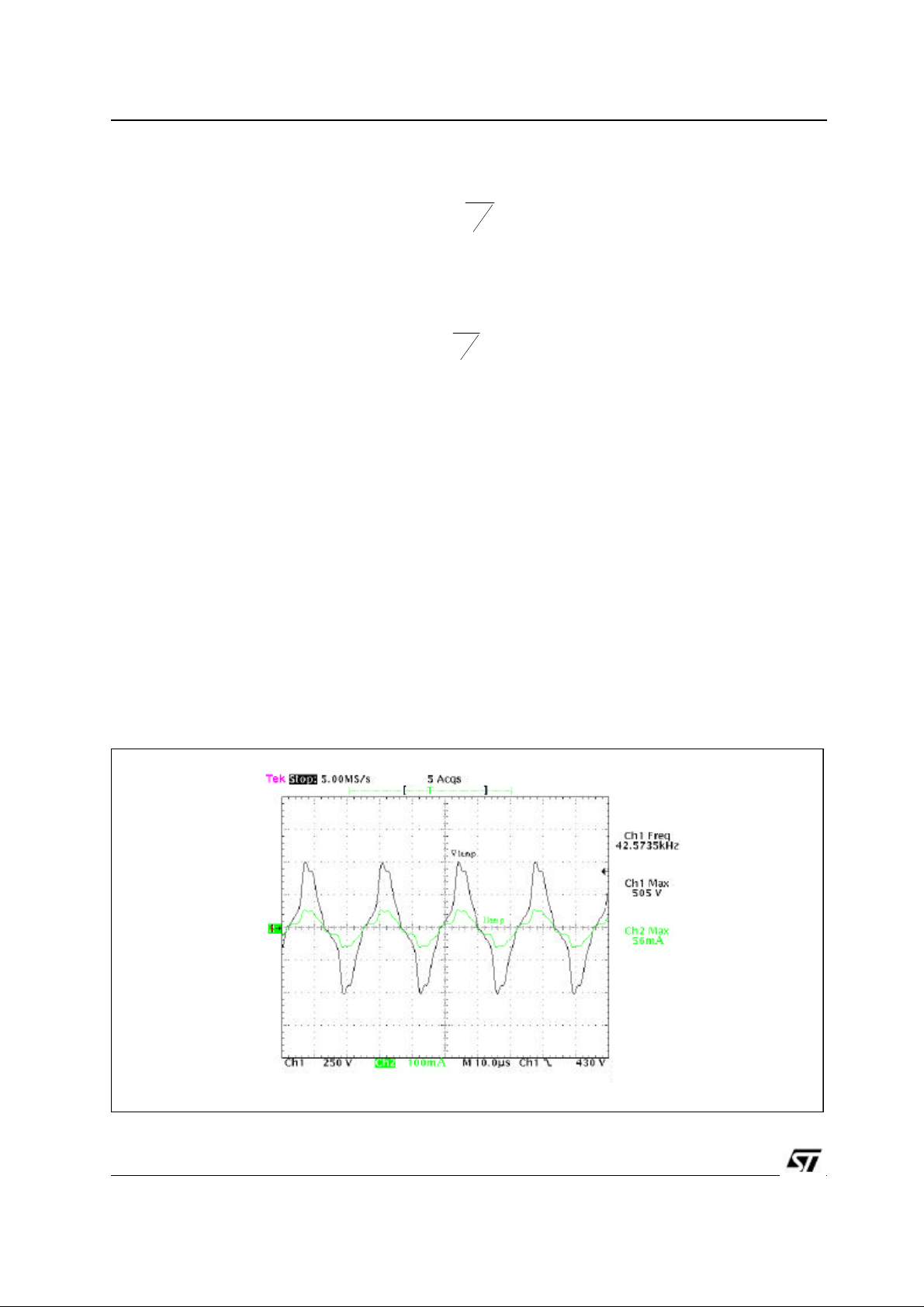
around 500V and the electrodes start to warm up and emit ions. Figures 1 and 2 show the V-time and Itime waveforms and the V-I waveform respectively before the start-up of a 24W tube.
Figure 1: V-time and I-time Waveforms Before the Striking
2/35
Page 3
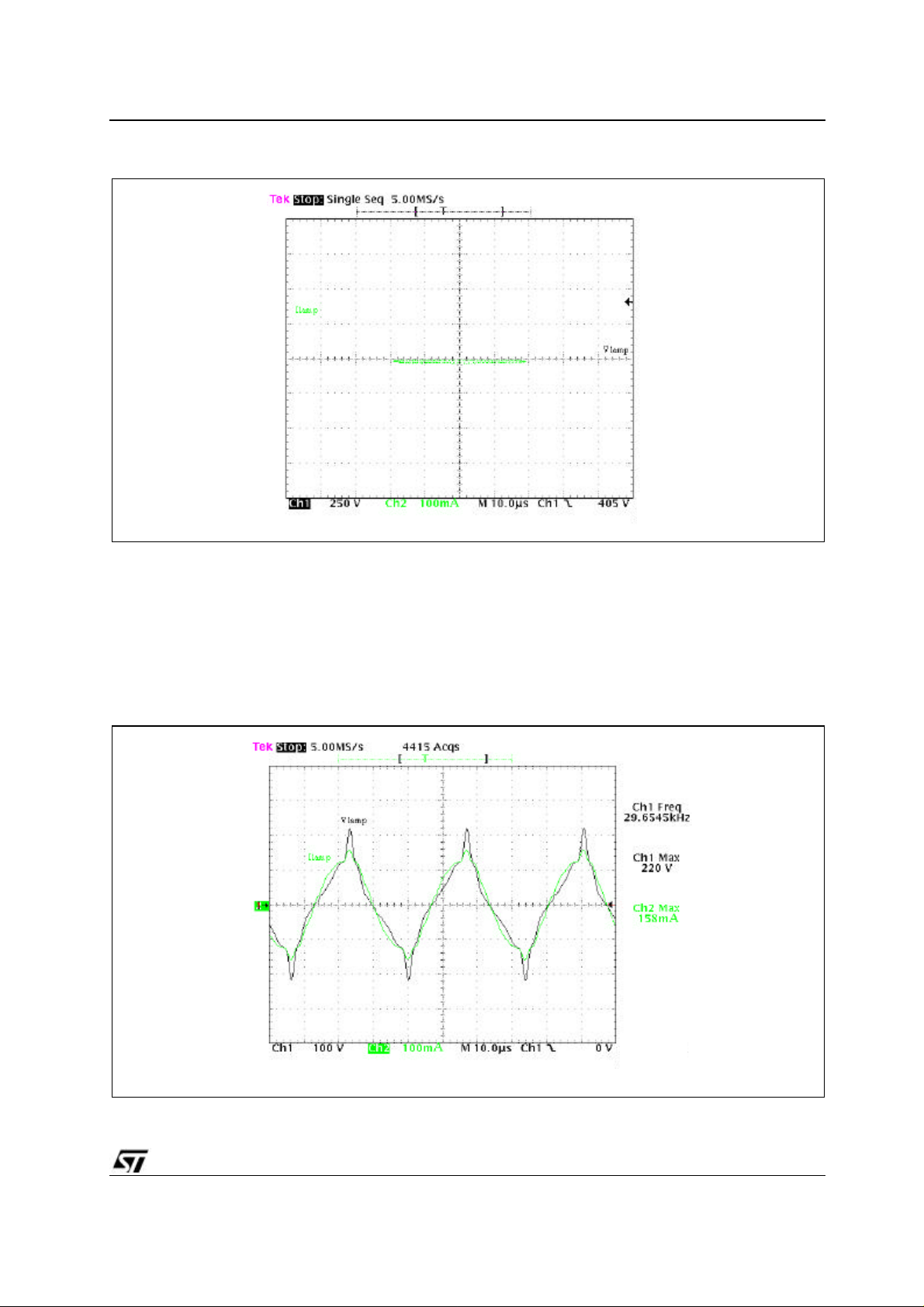
Figure 2: V-I waveform before the striking
AN1731 - APPLICATION NOTE
As shown above, to strike the fluorescent tube the electrodes voltage reaches up to 505V of peak.
Furthermore, the current that flows through the lamp is very low, 56 mA, because the resistance
before the striking is high (around 10 KOhm).
When the fluorescent lamp lights on, the gas mixture inside is fully ionized, and an arc across the
electrodes occurs. In this new condition, the lamp resistance drops to around 1 KOhm value (Figures 3
and 4 show the V-time and I-time waveforms and the V-I waveform after the striking.
Figure 3: V-time and I-time waveforms after the striking
3/35
Page 4
AN1731 - APPLICATION NOTE
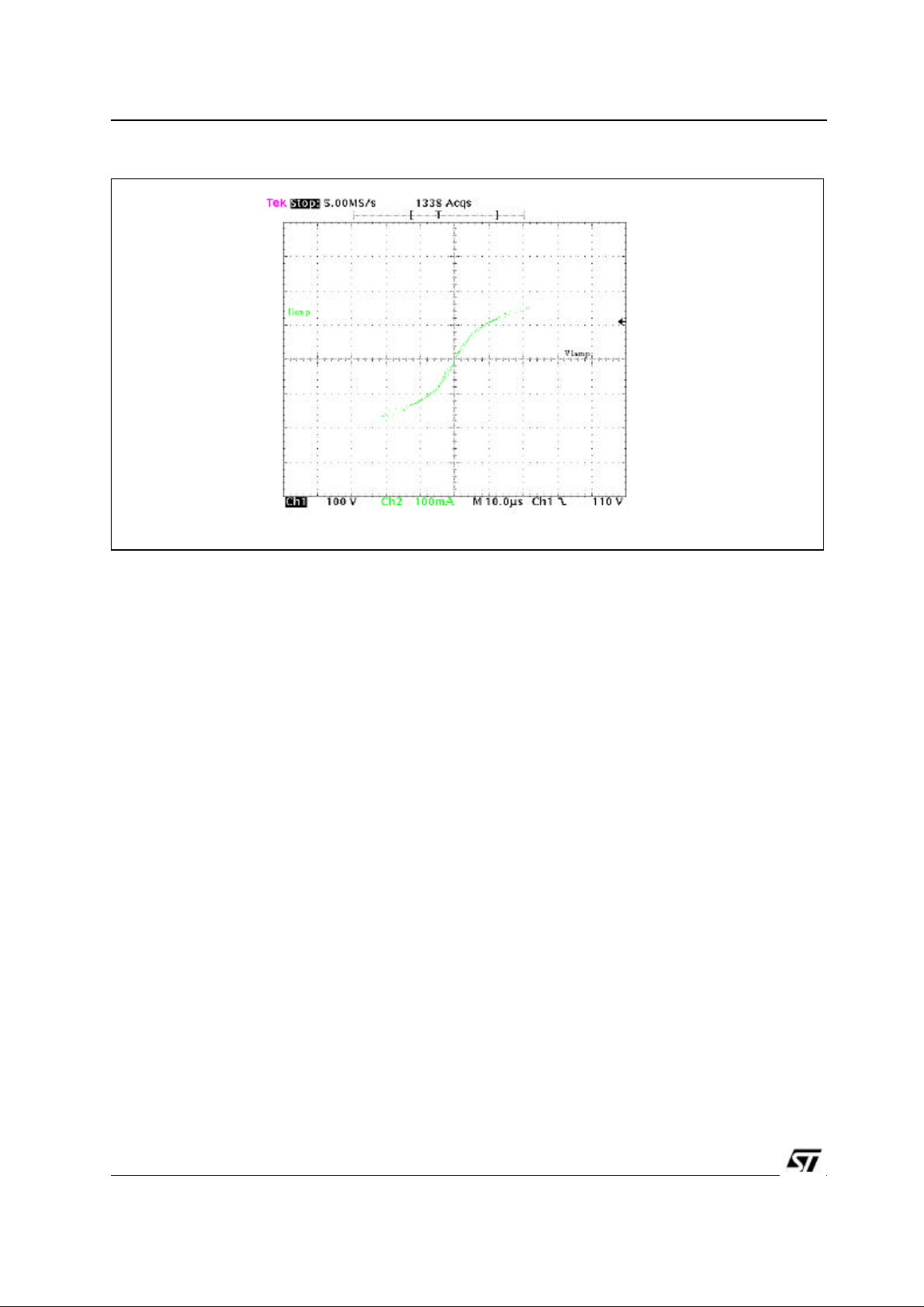
Figure 4: V-I waveform after the striking
After the striking, the gas mixture emits radiations that excite the fluorescent elements inside the tube
producing the light in the visible spectrum. In this example, after the striking, the voltage across the
electrodes drops from 505V of peak to 220V of peak and the current increases from 56mA of peak to
158mA of peak.
Usually, after the striking, in order to increase the lamp efficiency up to 15%, the operation frequency is in
the range of 25-30KHz. Furthermore, as shown in Fig. 4, the waveform I-V has a linear behavior until the
established voltage value is kept. In fact, if the voltage across the electrodes overcomes this established
voltage value, the characteristic becomes flat because no ion can emit other radiations.
4/35
Page 5
AN1731 - APPLICATION NOTE
2
2
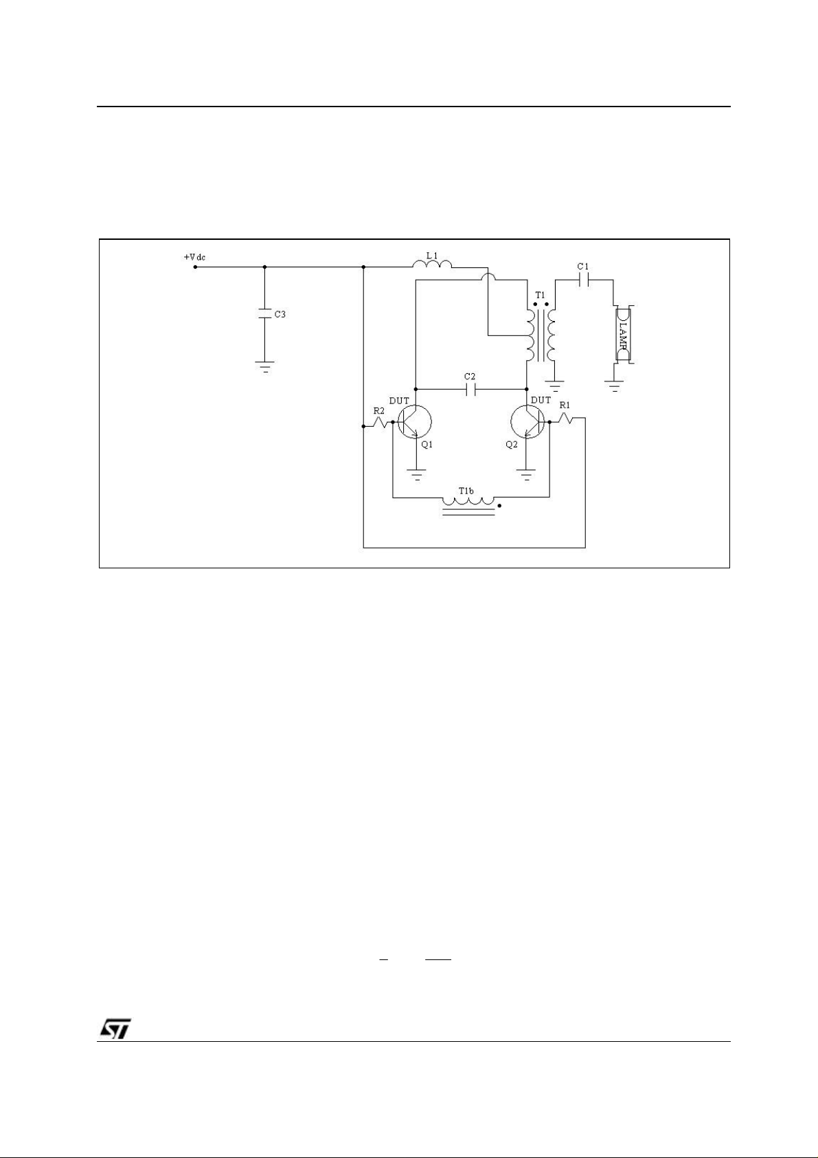
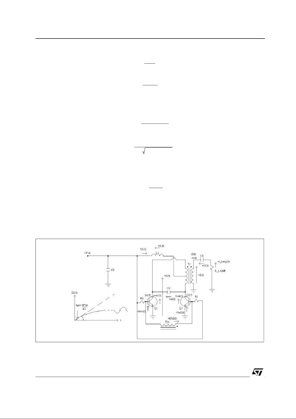
5. PUSH-PULL CURRENT FED CONVERTER TOPOLOGY INTRODUCTION
As previously exposed, a topology solution for emergency lighting applications is the PUSH-PULL current
FED converter topology. This topology solution has a Push-Pull switching converter forced to run in
synchronized mode by the inclusion of a supply inductor.
Figure 5: PUSH-PULL current FED converter schematic circuit
The components values of capacitors, resistors, and inductors are selected operation on the input voltage,
power lamp, and operation frequency.
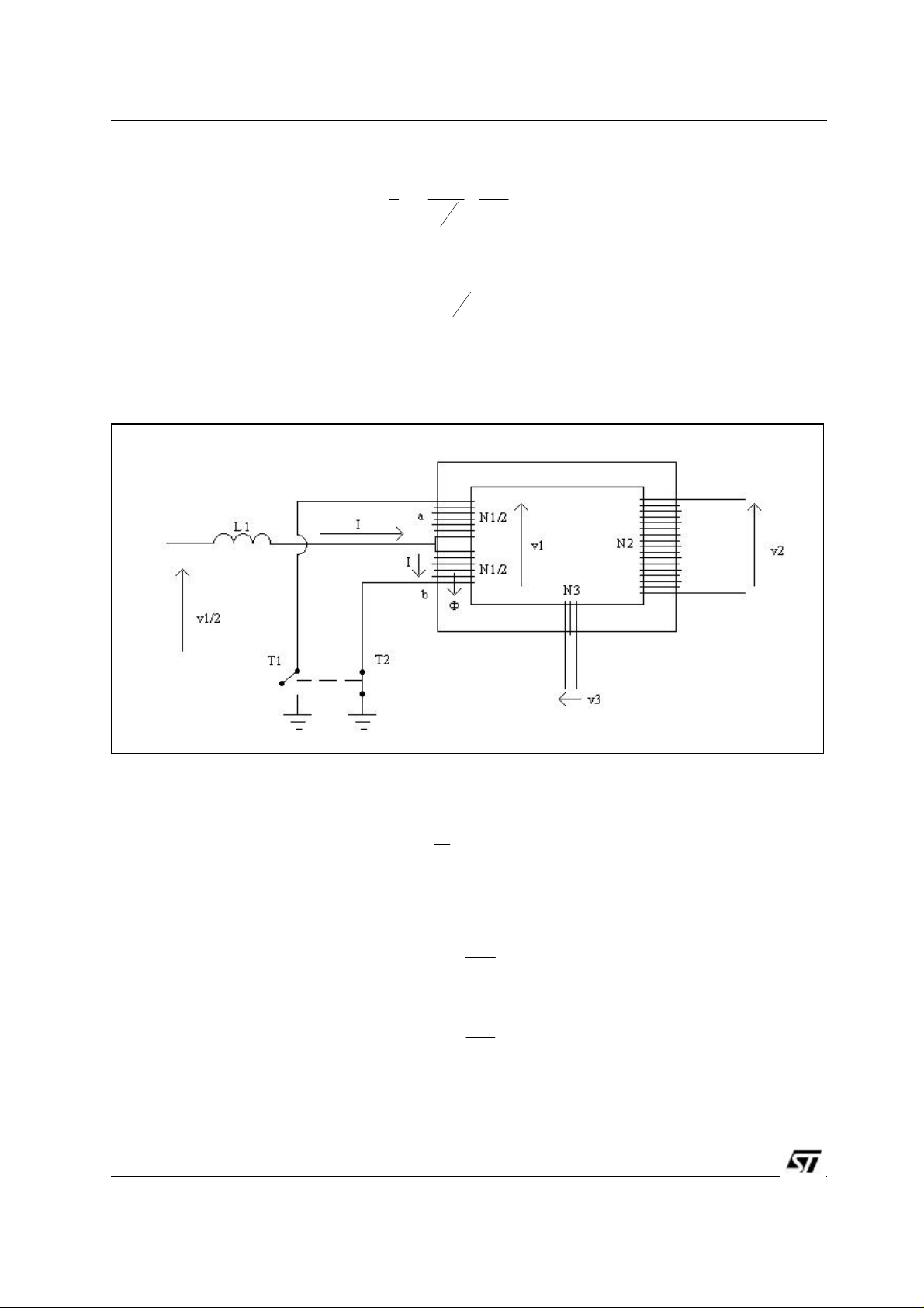
6. TRANSFORMER DESCRIPTION OF PUSH-PULL TOPOLOGY
In figure 5 the transformer named T1 has three windings. The primary winding vices are connected to the
collectors of the NPN power bipolar transistors Q1 and Q2. The same primary winding has a central vice
where the inductor L1 is connected. The secondary winding vices are connected to the load.
The third winding vices are connected to the base of the transistors Q1 and Q2 so that when the first is on,
the second is off and vice versa. During the Q2 on state, the current flows through the same device and
the respective half primary winding and vice versa. Usually the primary inductance LT of the transformer
T1 is much lower compared to the inductance L1. The resonance frequency of the PUSH-PULL converter
is also due to LT. N2 (secondary winding turns) and N1/2 (half primary winding turns) rapport is around 60,
while N1/2 and N3 (third winding turns) rapport is around 5. Considering a 6 Vdc input voltage, the voltage
v
(the max voltage across the vice of the primary winding central point and the reference) can be
1max
written as:
14.3
v
V
dcmax1
≅=⋅π=
(6.1)
V96
5/35
Page 6
AN1731 - APPLICATION NOTE
2
v
(the max voltage across the secondary winding vices) can be written as:
2max
N
v
v
(the max voltage across the vices of the third winding) can be written as:
3max
V
dcmax2
N
2
v
1
(
V
dcmax3
2
14.3
2
2
)
2
N
N
14.3
3
1
2
6
2
V560606
≅∗=⋅π=
1
V2
≅∗=⋅π=
5
(6.2)
(6.3)
As exposed above, it is highlighted N1/2 and not N1. In order to understand the reason of it, it is
necessary to consider the graph below.
Figure 6: Particular of T1
When Q2 is on, Q1 is off and vice versa. Now, considering fig. 6 where T2 is on; the current ‘I’ flows
through the half primary winding 'b' and it generates a magnetic force (Hopkinson law):
N
1
Φ⋅ℜ=⋅I
(6.4)
Φ is the magnetic flux and ℜ is the magnetic reluctance of the T1 core;Φ can be written as:
N
1
⋅=ΦI
2
(6.5)
ℜ
ℜ can be written as:
(6.6)
Al⋅=ℜµ
µ is the core permeability, A is the core section and l is the core length. When T2 switches off, T
switches on, the current flows through the other half primary winding 'a' and the flux Φ inverts its
direction. Such flux flows into the transformer core creating a link with N2, N3 and also with the other
6/35
1
Page 7
AN1731 - APPLICATION NOTE
∆Φ
=
=
=
turns N1/2, generating the voltages v2 and v3 (magnetic law-Lenz law):
Nv
−=
−=
v
2/1
v
N
v
2
2
v
1
,
N
v
1
2
;
22
t
∆
∆Φ
Nv
33
t
∆
N
∆Φ
1
−=
∆
2
N
3
3
N
1
1
2
(6.7)
;
t
v
2
c
2,
===
v
1
(6.8)
Furthermore, i2 (the current that flows through the lamp) can be written as:
N
1
1
2
Ii
2
I
==
K
N
2
(6.9)
In fact, the apparent input power can be written as:
in 1
IvA
(6.10)
The output power can be written as:
ivA
22
out
(6.11)
Considering an ideal transformer:
Iviv
122
(6.12)
i 1
I
2
12
v
2
===
2
kN
(6.13)
N
1
v
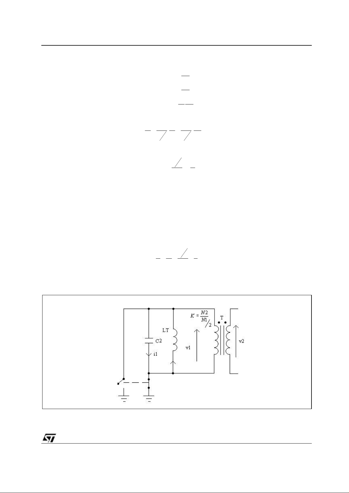
Before the lamp strike, or when the lamp is disconnected, the operation frequency (about 60 KHz) is due
to the resonance between C2 and the primary transformer winding inductance LT (see fig. 7).
Figure 7: Resonant Schematic Circuit Before the Lamp Strike
7/35
Page 8
AN1731 - APPLICATION NOTE
=
fπ⋅=
221LTC
(6.14)
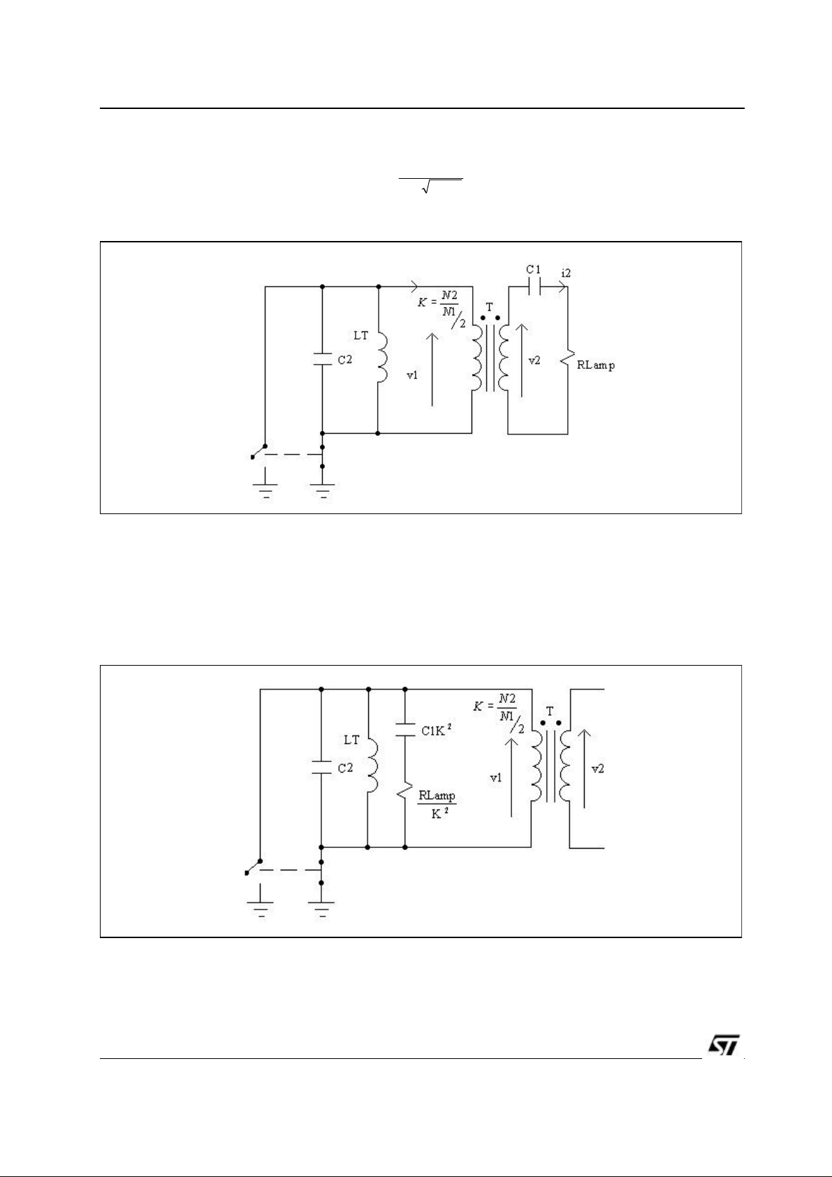
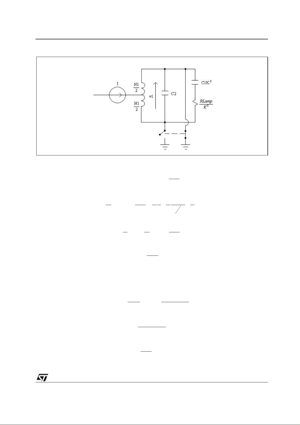
When the lamp is connected, the transformer circuit can be showed as in the graph below.
Figure 8: Ideal Schematic Circuit of the Transformer After the Lamp Strike
The input apparent power can be written as:
ivA
11in
(6.15)
Now it is possible to consider an equivalent circuit to fig. 8, as in fig. 9, where the apparent input power is
equal.
Figure 9: Equivalent Schematic Circuit of the Transformer After the Lamp Strike
Furthermore, after the lamp strike, the resonant schematic circuit can be represented as in figure 10
where, usually, the operation frequency is due to LT, C2 and C1K2 (25-30 KHz).
8/35
Page 9
AN1731 - APPLICATION NOTE
k
k
Figure 10: Resonant Schematic Circuit of the Transformer After the Lamp Strike
In this transformer equivalent circuit the output impedance has been transferred from the secondary
winding to the primary winding.
2
(
2221
Lamp
1
)
jRiivIv
−==
C
⋅
ω
1
(6.16)
Iv
1
( k
2
i
2
Lamp
v
jR
1
z
1
I
Where:
is the primary equivalent resistance and where:
is the primary equivalent capacitance.
Now, the equivalent primary admittance (Y
Y
eq
) can be written as:
eq1
j
−
=
ω
LT
⋅
and where:
is the admittance of the series net
1
V
1
)
1
1
k
ω
Lamp
(
2
R
LAMP
C1K
2
ω
jCR
2
Cj
2
−
Lampeq
2
21
Cjk+⋅
Lamp
iIi
22
−==
+⋅+
1
)1(
ω
2
kC
1
C
⋅−=ω
R
2
N
v
N
I
(
1
jR
C
⋅
ω
v
2
1
21
===
2
1
I
)
2
)
1
(6.17)
(6.18)
(6.19)
(6.20)
2
ω
Cjk
1
)1(
ω
jCR
+
Lamp
(6.21)
(6.22)
(6.23)
9/35
Page 10
AN1731 - APPLICATION NOTE
k
∆
Considering
R
Lamp
2
(6.24)
negligible compared to
(6.25)
deriving Y
compared to the pulsation and equal to zero, it is possible to achieve the frequency that
eq1
maximizes, the Y
1
2
kC⋅ω
1
(such frequency is the resonance frequency of the application during the lamps on
eq1
state).
2
≅ω
1
2
)(
CkCLT +
1
2
1
2
)(2
CkCLTf+⋅≅π
1
2
(6.26)
(6.27)
When the board is powered, R1 and R2 enable Q1 and Q2 and the lamp turns on. After the lamp start-up,
during the Q2 on state, the current flows through L1, the half primary winding transformer T1 and Q2, and
it increases as:
*Ltv
1
L
tg
=α
1
(6.28)
angular coefficient but, after a while, the current curves and it becomes flat. However, in the permanent
state, even if the current oscillates around its average value, there is a ripple of this same value. The
current ripple decreases increasing the inductance value L1.
Figure 11 shows the PUSH-PULL current FED converter schematic circuit with the theoretical waveform
of ‘I’.
Figure 11: PUSH-PULL Current FED Converter Schematic Circuit with the Theoretical Waveform
10/35
Page 11
AN1731 - APPLICATION NOTE
After the strike, ‘I’ generates the current i2 and, at the beginning, the same i2 can be written as:
v
2
i
=
2
R
Lamp
(6.29)
because the capacitor C1 is discharged. Immediately after, C1 gets charged and i2 decreases to zero
until the voltage across C1 reaches the maximum value. A this time, the current i2 inverts its direction and
the capacitors C1 start discharging until the charge inside it becomes zero and the current i2 reaches its
maximum negative value. Furthermore, when i2 inverts itself, also the voltage across the third winding
inverts its direction so that Q2 switches off and Q1 switches on and ‘I’ flows through the other half primary
winding of the transformer T1 (see fig. 11).
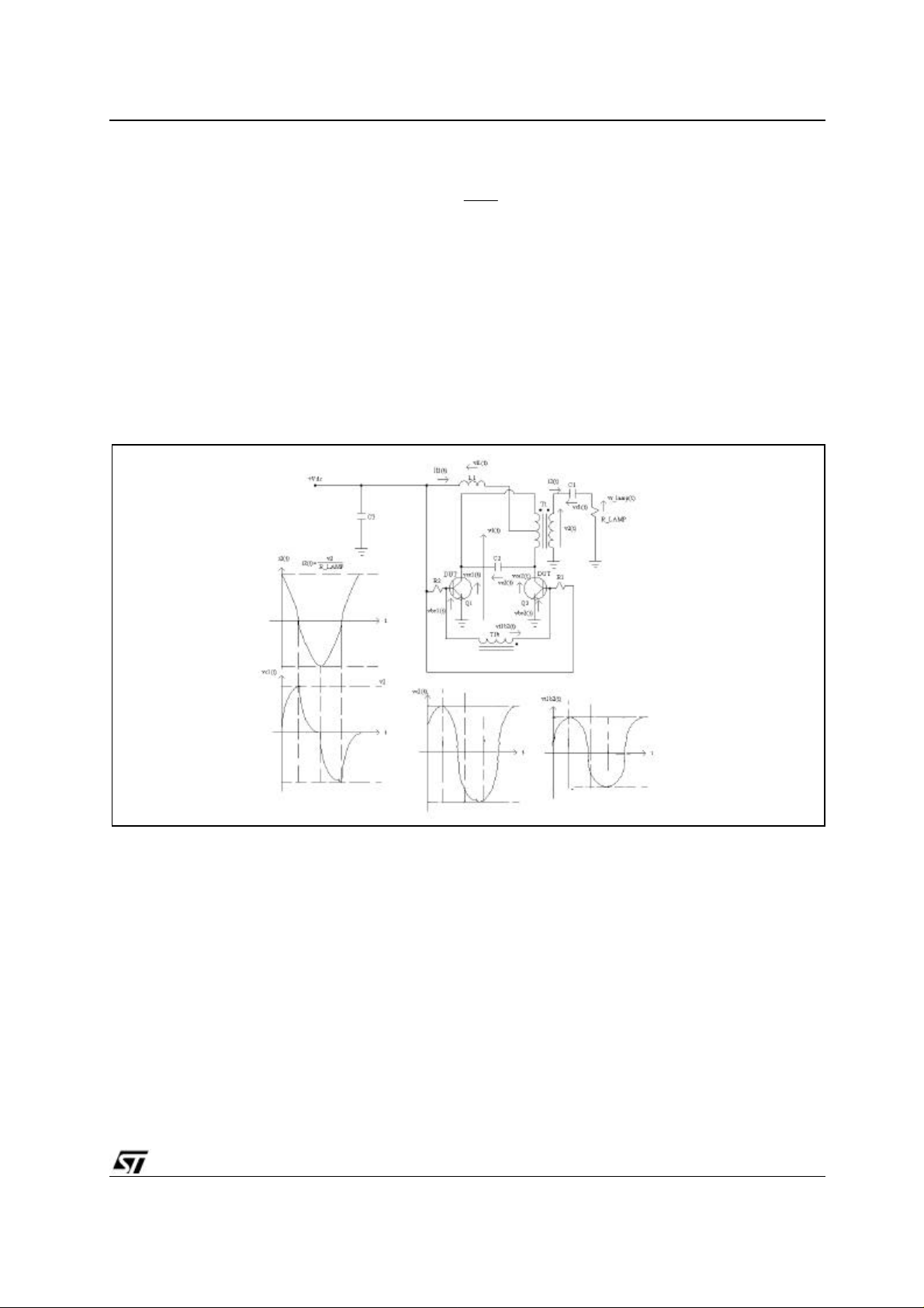
Figure 12: PUSH-PULL Current FED Converter Schematic Circuit with vc1, vc2, i2, and v
t1b2
Theoretical Waveforms
In the above graph, vc2 is the voltage between the vices of the Q1 and Q2 collectors. The maximum value
of such voltage is twice v1, where v1 is the voltage between the vices of the central point of the primary
winding of T1 and the reference. The voltage v1 is a half positive sine wave and this reaches the
maximum value when Q1 or Q2 are on, while it drops to zero during the turn-off and the turn-on of the
same transistors (see fig. 13).
11/35
Page 12

AN1731 - APPLICATION NOTE
2
Figure 13: PUSH-PULL current FED converter schematic circuit with vc2, v1, and vL1 theoretical
waveforms
The figure above also highlights the vL1 voltage. This is the voltage across L1 and it is achieved
considering the difference between Vdc and v1.
Now focusing the attention on only one half-period of v1 as showed in fig. 14, it is evident that the area
A2 must be equal to the area A1 because v1 and Vdc must have the same average value.
Figure 14: v1 waveforms
A1 can be written as:
1TVAdc=
12/35
(6.30)
Page 13

A2 can be written as:
T
2
2
π
⋅=π
AN1731 - APPLICATION NOTE
T
2
∫
0
π
==
)2(max12
senVA
tdt
T
(6.31)
T
2
T
V
max
2
π
2
π
cos([1
T
])
V
t
=−=
max1
π
0
considering: A1=A2
(6.32)
TT
V
π
v
can be written as:
c2max
max2
v
is also the maximum voltage value between the collector-emitter vices of Q1 or Q2.
c2max
VV
VVV
=⇒=
max1max1
dc
dc
(6.33)
(6.34)
The theoretical voltages and the currents waveforms of Q1 or Q2 are shown below.
Figure 15: Q1 and Q2 theoretical waveforms
Ic1 and Ic2 can be written as:
N
2
IIc=
max2max1
N
1
2
I
2
max2
)
(
RP
=
Lampout
2
(6.35)
(6.36)
13/35
Page 14

AN1731 - APPLICATION NOTE
∆=−=−
=
T
−−+
+=+
BA=
ADB
C
=
=
I 2
=
max2
P
out
R
Lamp
(6.37)
N
=
N
and I
2
1
2
b2on
R1 and R2 can be also used to adjust the I
I 2
c
max1
b1on
Now focusing the attention on only one half-period of vL1:
Figure 16: vL1 theoretical waveform detail
P
out
R
Lamp
(6.38)
.
After the lamps strike ‘I’ fluctuates around its average value:
minmax
because:
0
v
med
where v
v
med
is the average value of L1.
med
can be written as:
v
=
med
T is the period of vL1.
CBDA
,
14/35
IIIII
(6.39)
(6.40)
CBDA
)(
(6.41)
(6.42)
(6.43)
(6.44)
Page 15

vL1 can be written as:
2
T
ππ⋅
2
T
ππ⋅
2
∆
t
∆
ax
∆
2
∆
4'{'
T
t
π
⋅
π
⋅
AN1731 - APPLICATION NOTE
t' is the time when vL1 is zero:
Considering that:
Considering the Lenz law:
It is possible to achieve L
(the minimum L1 value that allows the established current ripple to be
min
obtained) as:
During the time interval 0-t' I increases by:
2
(
senVVv
T
=
=
dcdcL
senVV
⋅−=
dcdc
arcsen
=∆
%max
med
Lv
min1
t
Im
∆
I
max
⋅−=
2
(
)2(
ππ
I
max
I
med
III
∆=⋅∆
max%max
I
max
∆
v
med
1
0 t
'
t⋅=
I
med
L
min1
)
t
)'
(6.45)
(6.46)
(6.47)
(6.48)
(6.49)
(6.50)
(6.51)
(6.52)
v
can be written as:
med
L
can be written as:
1min
'
t
1
v
L
1
Lmed
'
t
0
1
v
2
=
min1
I
∆
max
'
t
1
dtv
[
∫∫
'
t
0
T
tV
'{
tV
dcdc
2
cos(1[
V
−−⋅=
dcdcmed
T
4
cos(1[
V
−−⋅
dcdc
⋅
2
⋅−=⋅=
ππ
)]
(
senVV
2
2
T
dtt
T
)]}'
t
)]}'
t
(6.53)
(6.54)
(6.55)
15/35
Page 16

AN1731 - APPLICATION NOTE
7. EXAMPLE OF AN EMERGENCY LAMP APPLICATION
The following example takes into consideration a real emergency lamp application with a PUSH-PULL
current FED converter topology using a 24W lamp and powered with 6 Vdc with STSA851.
The graph below shows Ic, Ib, and Vce waveforms of the STN851 device when the lamp is connected.
Figure 17: Steady state of STSA851
The following graphs show the turn-off and turn-on switch modes respectively.
Figure 18: Turn-off of STSA851
16/35
Page 17

AN1731 - APPLICATION NOTE
Figure 19: Turn-on of STSA851
In these graphs it is possible to see that the operation frequency is around 30KHz, Ic is around 2.4A and
that I
is around 70mA. The Ib spike during the turn-on switch mode is due to the collector-base
bon
junction charge, while, the negative Ib spike during the turn-off switch mode is due to the storage charges
extraction. Furthermore, in this example, during the turn-off switch mode, the dissipated energy is due to
a C2, discharging on the power bipolar device, that decelerates Ic decreasing. Sometimes, in order to
decrease the turn-off dissipated energy, two capacitors between the vices of the collector-emitter of both
devices are connected.
The figure below shows the steady state of the STSA851 device without the lamp.
Figure 20: Steady state of STSA851 without the lamp
In this case the operation frequency is around 60 KHz.
The current and the voltage values measured on the power bipolar device are inside the STSA851
specifics.
17/35
Page 18

AN1731 - APPLICATION NOTE
The next graphs show the vL1, ‘I’ and v
waveforms with and without lamp respectively.
c2
Figure 21: vL1 and I Waveforms With Lamp Connected
Figure 22: vc2 Waveform With Lamp Connected
18/35
Page 19

Figure 23: vL1 and I Waveforms Without Lamp Connected
Figure 24: vc2 Waveform Without Lamp Connected
AN1731 - APPLICATION NOTE
19/35
Page 20

AN1731 - APPLICATION NOTE
8. FORWARD VOLTAGE FED CONVERTER TOPOLOGY
As previously exposed, another topology solution for emergency lighting applications is the FORWARD
voltage FED converter solution that uses a transformer with three windings.
Figure 25: FORWARD Voltage FED Converter Schematic Circuit
As shown in the PUSH-PULL current FED converter solution, the components values of capacitors,
resistors, and inductors are designed in order to have an operation frequency of around 30 KHz, after the
lamp strike and before too, in order to supply the right voltages to the load before and after the lamp
strike considering the voltage value of the battery.
When the board is powered, a suitable trigger circuitry, usually consisting of a small signal bipolar
transistor and a resistor, enables Q1 and, immediately after, a current flows through the V
primary
tr2a
winding of the transformer Tr2 and the same transistor. During the Q1 on state, the input battery voltage
Vdc is applied to the V
T
, in fact, the coils number of the both windings is the same, but no current flows through T
r2b
because the diode D2 is disabled. At the same time, a voltage appears in the winding V
flows through the same winding depending on the output impedance. The V
vices winding and the same voltage appears in the vice of the second winding
tr2a
and a current
tr2c
voltage depends on the
tr2c
r2b
input voltage battery Vdc by means of the N2/N1 rapport.
In particular, V
I
, the RMS of the primary winding current, can be written as:
1eff
where N1 and N2 are the turn numbers of V
can be written as:
tr2
tr2a
and V
N
2
VV =
dcc2tr
N
1
N
2
II =
eff2eff1
N
1
respectively, I
tr2c
(8.1)
(8.2)
is the RMS of the lamp current
2eff
and can be written as:
where Zeq is the output impedance.
20/35
I =
eff2
V
c2tr
Z
eq
(8.3)
Page 21

AN1731 - APPLICATION NOTE
At the beginning, before the lamp strike, the lamp resistance is very high and the equivalent circuit can be
showed as in the figure below.
Figure 26: Schematic Circuit Before the Lamp Strikes
Usually, the capacitor value of C3 is higher compared to the same of C2, so that the simplified schematic
circuit can be showed as in fig. 27.
Figure 27: Simplified Schematic Circuit Before the Lamp Strikes
21/35
Page 22

AN1731 - APPLICATION NOTE
It is also possible to consider an equivalent circuit as in fig. 28 where the output impedance is transferred
in the primary of the transformer.
Figure 28: Equivalent Schematic Circuit Before the Lamp Strikes
The series net K2C2-L2/K2 can be written as:
2
L
⋅ω
2
j
K
1
j
−
⋅ω
j
=
22
CK
2
1CL
−ω
22
2
CK
⋅ω
(8.4)
2
The equivalent impedance can be written as:
3
jZ
=
eq
2
L?CLL?
⋅−
1221
2
2
12
(8.5)
1)LK(LC?
−+⋅
Deriving Zeq from ω it is possible to obtain the resonance frequency.
∂Zeq/∂ω = 0 (8.6)
ω2 = 1/L2C
⇒f = 1/ 2⋅π √L
2
2C2
(8.7)
22/35
Page 23

AN1731 - APPLICATION NOTE
In order to know the resonance frequency after the lamp starts up, it is necessary to consider the
schematic circuit with a short circuit condition.
Figure 29: Schematic circuit considering a short circuit condition
23/35
Page 24

AN1731 - APPLICATION NOTE
Furthermore, it is possible to consider the equivalent schematic circuit as in fig. 30 transferring the output
impedance in the primary winding.
Figure 30: Equivalent Schematic Circuit Considering a Short Circuit Condition
The resonance frequency in this condition can be written as:
1
2
?
f
=⇒=
2
KCL
21
1
⋅
21
(8.8)
2
KCLp2
Usually, the resonance frequency considering the output short circuit condition is lower compared to the
resonance frequency before the lamp start-up condition. The resonance frequency after the
lamp start-up has got a value which is between the frequency before the lamp start-up and the output
short circuit frequency.
1
⋅
f
2
KCLp2
21
1
<<
⋅
(8.9)
CLp2
22
However, after the start-up, the resonance frequency is almost equal to the resonance frequency before
the lamp start-up. Fig. 31 shows the resonance frequency after the lamp start-up considering several
loads.
24/35
Page 25

AN1731 - APPLICATION NOTE
=
Figure 31: Resonance Frequency After the Lamp Start-up vs. Resistance Load
During the positive half-wave, i2 is the same as Ib because this flows through the base of the power
bipolar transistor; instead, during the negative half-wave, when the current inverts its direction, i2 flows
through the net R1- D1. At the same time, the voltages across T
r2a
, T
and T
r2b
windings invert their
r2c
directions, Q1 switches off, Ic drops to zero, and Vce increases up to:
V2V
dcce
(8.10)
the sum of the input battery voltage Vdc and the third winding voltage:
VV =
dca2tr
(8.11)
However, after Q1 switches off, an extra-voltage can appear across collector-emitter vices due to a quick
decrease in the Ic that flows through the V
winding. In order to avoid this effect, V
tr2a
enables D2 and
tr2b
the current passing through it creates a magnetic force N3I3 opposed to N1Ic (N3 and I3 are the turn
number and the current that flows through T
r2b
).
25/35
Page 26

AN1731 - APPLICATION NOTE
The graph below shows the output schematic circuit and the theoretical waveforms before the lamp
strike.
Figure 32: Output Schematic Circuit Before the Lamp Strike and Theoretical Waveforms of the
Main Output Electrical Parameter
The voltage across V
generates an i2 having the same phase. vc2 (the voltage across C2) is
tr2c
+90° out-phase compared to the i2, while vL2 (the voltage across L2) is -90° out-phase compared to i2.
The graph below shows the Ib, Vce and Ic theoretical waveforms of Q1.
Figure 33: Q1 Theoretical Waveformsr
Note: a circuit similar to the Forward Voltage FED Converter shown in Fig. 25 is also described in
the Italian Patent N.1285621 in the name of Beghelli S.p.A.
26/35
Page 27

AN1731 - APPLICATION NOTE
∆Φ
t
∆Φ
∆
9. TRANSFORMER DESCRIPTION
The transformer has three windings. The primary winding vices are connected to the input voltage and
the other vice to the collector of Q1, while the secondary winding vices are connected to the load. The
third winding vices are connected between the input voltage and the cathode of D2. The schematic of the
transformer can be shown as in fig. 34.
Figure 34: Transformer Detailr
The FORWARD converter works during the Q1 on state (in this graph the switch T1 is the equivalent
component of Q1). In such operation condition, current flows through the turn N1 and a flux is generated.
IN
1
=Φ
ℜ
(9.1)
This flux flows through the magnetic core of the transformer creating a link respectively with the turns N
and N3 and it generates the voltages v2 and v3.
Nv
−=
33
t
∆
Nv
−=
22
∆
(9.2)
(9.3)
However, during the Q1 on state, no current flows through the third winding because the diode D2 is
disabled, while output current flows through the secondary winding and the load. The voltage across the
primary winding, equal to Vdc, can be written as:
I
LVv
−==
m1dc1
t
on
(9.4)
Lm1 is the inductance of the primary winding and ton is the time during the Q1 on state.
When the secondary winding current inverts its direction, Q1 switches off, the current ‘I’ suddenly
2
27/35
Page 28

AN1731 - APPLICATION NOTE
=
becomes zero and an overvoltage appears across the turn N1. However, during the Q1 switching off, a
magnetic force appears across the third winding opposing the primary winding magnetic force and
avoiding the extra voltage on Q1 (see fig. 35).
ININ
331
(9.5)
Figure 35: Transformer Detail When T1 Switches on
It is important to highlight that the current ‘I’ is the sum of the currents Im and I' (see fig. 36). The extra
voltage on Q1 is due to Im.
Figure 36: Detail of the Transformer Highlighting Im1 and I'
28/35
Page 29

AN1731 - APPLICATION NOTE
In the FORWARD converter it is important to consider the right turn N3 and the right duty cycle, it is
possible to have an increasing current Im and a saturation of the transformer core might occur.
Figure 37: Theoretical Behavior of Im Involving the Transformer Core Saturation
In fact, the B-H characteristic, where B is the induction vector and H is the magnetic vector, can be
represented as in fig. 38.
Figure 38: Theoretical B-H characteristic
H can be written as:
H1=
IN
l
(9.6)
When 'I' increases then also H increases, and if H overcomes an established value even if H keeps
increasing, B remains constant.
In order to avoid the core saturation, it is necessary to choose a right N3 and duty cycle. The right limit
29/35
Page 30

AN1731 - APPLICATION NOTE
∆Φ−=∆Φ
2
case is shown in fig. 39.
Figure 39: Theoretical Behavior of Im Considering the Right Limit Case
In this condition, v1 and v3 can be written as:
NVvv
−===
1dc31
t
t
N
N
1
t
on
on
3
N
N
t
1
off
t
on
==δ
T
1
N
3
t
on
off
t
off
t
T
on
−==⇒=
N
N
3
33
1
N
3
+
N
1
(9.7)
(9.8)
(9.9)
Usually, N1 and N3 are equal so that the minimum duty cycle that avoids the saturation of the core is:
1
=δ
(9.10)
The Emergency Lamp applications using the FORWARD topology work in resonance mode and their
duty cycle is, obviously, 0.5.
10. EXAMPLE OF AN EMERGENCY LAMP APPLICATION WITH FORWARD TOPOLOGY
The following example analyzes a real emergency lamp application with FORWARD voltage FED
converter topology using 8W lamp and powered with 3.6 Vdc and using also STSA851 (when the
application is powered with the battery the output power on the lamp is around 30% of the nominal power
lamp). In the graph below the steady state of Q1, after the lamp strike, is showed.
30/35
Page 31

Figure 40: Steady State of STSA851
AN1731 - APPLICATION NOTE
The following graphs show the turn-off and the turn-on switch modes respectively.
Figure 41: Turn-off of STSA851
31/35
Page 32

AN1731 - APPLICATION NOTE
Figure 42: Turn-on of STSA8511
The graph below shows the waveforms of V
Figure 43: Voltages on V
tr2a
, V
tr2b
and V
, V
tr2a
tr2b
Windings1
tr2c
and V
after the lamp strike.
tr2c
32/35
Page 33

AN1731 - APPLICATION NOTE
During Q1 on state, the voltage on V
observed, instead, during Q1 off state noise is highlighted on V
is imposed by the battery (Vdc=3.6 V) so that no noise is
tr2a
tr2a
and V
. The next graph shows the
tr2b
waveforms of the electrical parameters considering the output impedance after the lamp strike.
Figure 44: V
, Vc2, VL2 and i2 Waveforms1
tr2c
The graph below shows the lamp current and the current Ib waveforms.
Figure 45: i2 and Ib Waveforms
33/35
Page 34

AN1731 - APPLICATION NOTE
The graphs below show the steady state of Q1 and the electrical parameters waveforms of the output
stage before the lamp strike.
Figure 46: Steady State of STSA851 Before the Lamp Strike
Figure 47: I2, V
tr2c
, V
tr2a
and V
Waveforms Before the Lamp Strike
Lamp
34/35
Page 35

AN1731 - APPLICATION NOTE
11. CONCLUSIONS
Today the Emergency Lighting applications are used in all public places and private homes due to new
safety rules. Such applications use fluorescent tubes and are powered with 3.6 Vdc or 6 Vdc input
voltages. Usually, the output power can be 8W or 24W but, sometimes, the Emergency Lamp
applications can be used also to drive 58W fluorescent tubes. In this last case, however, the applications
supply only around 10-15% to the nominal lamp power. The main topologies used are PUSH-PULL
current FED and FORWARD. In the first solution, the frequency before the lamp strike is about 60 KHz,
while after the lamp strike is about 30 KHz, the current Ic is about 2.5A, Ibon around 80mA and Vcemax
around 15V considering an input voltage of 6Vdc. Using the second topology solution and a 3,6Vdc input
voltage, the current Ic is about 1,7A, Vcemax 10V, Ibon around 70mA and the operation frequency,
before and after the lamp strike, is around 30 Khz. However, considering both topology solutions, the
power bipolar device STSA851 can be used because the voltages and currents values are inside the
SOA area.
Information furnished is believed to be accurate and reliable. However, STMicroelectronics assumes no responsibility for
the consequences of use of such information nor for any infringement of patents or other rights of third parties which may
result from its use. No license is granted by implication or otherwise under any patent or patent rights of
STMicroelectronics. Specifications mentioned in this publication are subject to change without notice. This publication
supersedes and replaces all information previously supplied. STMicroelectronics products are not authorized for use as
critical components in life support devices or systems without express written approval of STMicroelectronics.
The ST logo is a registered trademark of STMicroelectronics.
All other names are the property of their respective owners
© 2004 STMicroelectronics - Printed in Italy - All rights reserved
STMicroelectronics GROUP OF COMPANIES
Australia - Belgium - Brazil - Canada - China - Czech Republic - Finland - France - Germany - Hong Kong - India - Israel
- Italy - Japan - Malaysia - Malta - Morocco - Singapore - Spain - Sweden - Switzerland - United Kingdom - United States
http://www.st.com
35/35
 Loading...