

Page 1
AN1729
APPLICATION NOTE
L6565-BASED LOW COST SMPS FOR TV WITH
LESS THEN 1W STANDBY CONSUMPTION
by: R.D. Stracquadaini, C. Leonardi
The need for energy consumption reduction brings to the design of more and more efficient power supplies. High efficiency is required not only when the system supplied is fully operating but also when it is
in standby condition and absorbs very little power. A common design target for many home appliances
is that their power consumption in standby mode be less than 1W.
In this paper a cost-effective solution for the power supply of a 60W 14" TV, with a standby power consumption of less then 1W is presented.
The topology used for t his Switch Mode Power Supply is a Quasi-resonant Flybac k Converter (See
AN1326) in order to reduce the switching losses (ZVS at turn-on) and then to increase efficiency. In order to increase the performance in standby condition the start up network was designed with particular
care and the 2
burst mode operation of the power supply when the system is in standby condition. The power MOS
STP7NK80 (BV
nd
level of overcurrent protection of the L6565 QR controller is used to obtain an enhanced
= 800V, R
DSS
= 1.5Ω ) is used as the power switch.
DSon
QR ZVS Flyback topology
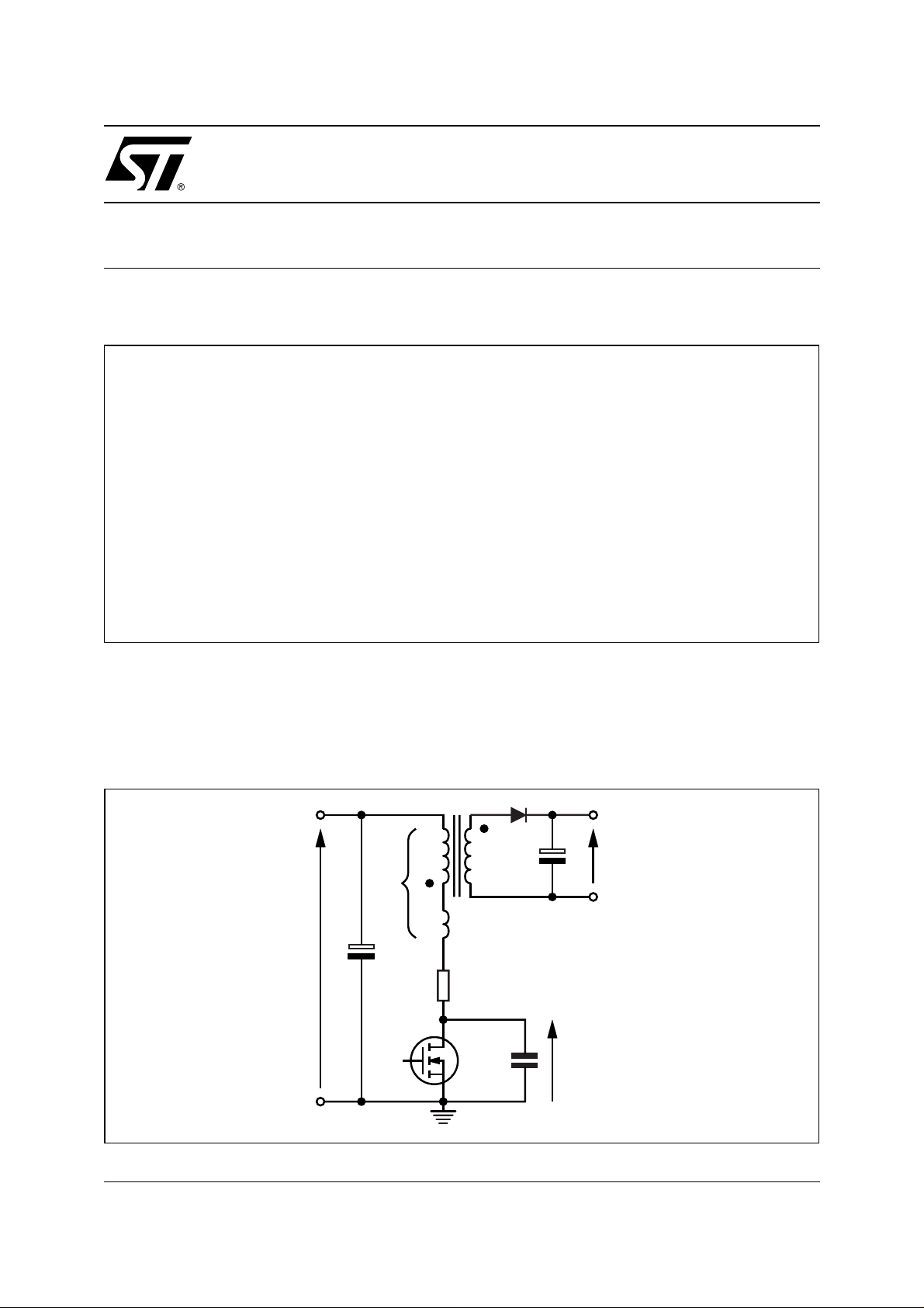
In figure 1 a typical Flyback topology is illustrated. CD is the total capacitance of the drain node. It is the sum of
the Mosfet' s C
well as other contributions reflected from the secondary side.
Figure 1. Flyback topology
transformer intrawinding capacitance, st ray capacit ance due to the layout of t he ci rcuit as
OSS,
Vin
Lm Ls
Lp
Llk
Cin
Rp
Cd V
Vout
DS
D03IN1462
June 2003
1/10
Page 2
AN1729 APPLICATION NOTE
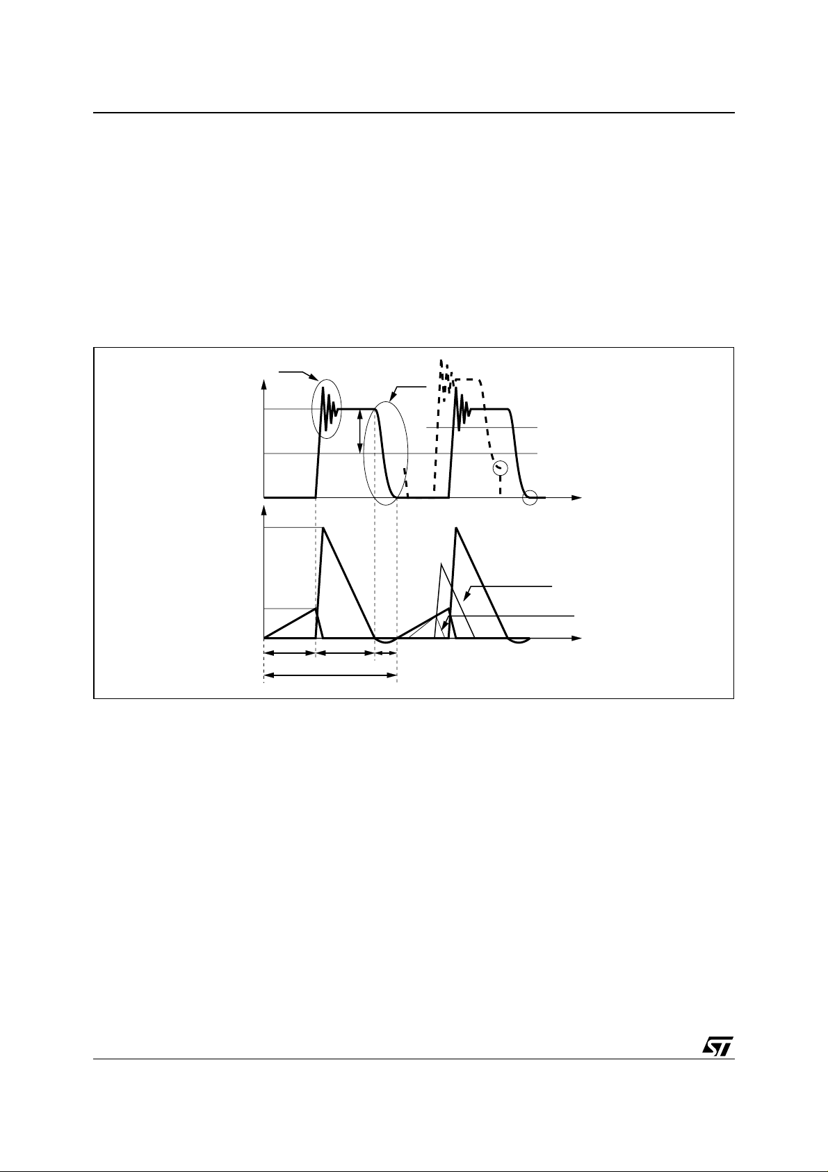
The Power Mos is turned off when the drain current reaches a threshold that is fixed by the controller depending
on the input and the out put v oltages. A s the secondary wi nding has run dry of energy, t he secondary rectif i er
no longer conducts and the Power Mos is still off, the tank circuit, made up L
It is an RLC circuit (considering the sum of dissipative effects concentrated in a equivalent resistor R
drain voltage follows the natural evolution of such circuit starting from the condition of C
= 0 (see waveforms in figure 2). R
is normally by far less than the critical damping impedance of the tank circuit.
P
At the point where the drain voltage has a valley (a minimum) we can turn on the Power MOS and we can have
a zero voltage turn on (if V
≤
VR) or a turn on where VD is as close as possible to zero compared w ith a square
in
wave flyback (see figure 2). This is Quasi-resonant (QR) operation.
Figure 2. Typical waveform s of QR operation
Llk & C
d
V
DS
V
DSs
V
V
in
L
& C
p
d
R
and CD, resonates.
P
VDS @ V
in2 >Vin
V
in2
charged at V
D
) and the
P
DSs
at t
in2 >Vin
Ip @ V
D03IN1463
ZVS
t
in2 >Vin
I
I
I
PKs
PKp
NO ZVS!
p
P
ri
T
ON
T = 1/f
Sec
Is @ V
T
sw
FW
T
V
The main advantages of this kind of control technique are:
1) At turn-on of the Power Mosfet the energy stored in the capacitor C
itself. Being the energy stored in C
proportional to V
D
2
, turning on the Mosfet when VD is minimum means
D
is dissipated into the power Mosfet
D
minimizing this kind of losses.
2) Probably the main benefit concerns the conducted EMI emission. In mains-operated applications, due to the
ripple appearing across the input bulk capacitor, the sw itching frequency is modulated at twice the mains
frequency, with a depth depending on the ripple amplitude. This causes the spectrum to be spread over frequency bands, rather than to be concentrated on single frequency values. Especially when measuring conducted emissions, with the average detection method, the level reduction can be of several dB
µ
V.
3) Another important be nefit is a high safety degree under short circuit conditions: since t he conduction cycles
of the Mosfet are inhibited until the transformer is full y demagnetised, flux run away and, therefore, transformer saturation are not possibl e. Moreover, as during a short ci rcuit the demagnetisation voltage i s v ery
low, th e s y ste m w ill be led to w o rk at v ery lo w fr equenc y, with a very s mall duty cycle. As a result, the power
that the converter will be able to carry is very low.
4) Finally, the way the system processes power does not change, thus designer's experience with standard
Flyback can be fully exploited and there is very little additional know-how needed.
2/10
Page 3

AN1729 APPLICATION NOTE
For further information concerning a QR Flyback converter based on controller L6565 you can refer to the Application Note AN1326 and to the datasheet of the controller.
Standby Consumption Issues
When the TV set is in standby we need to supply the m icro controller, the LED and the IR receiver for the remote
control. This supply voltage can be obtained through a linear voltage regulator from one of the low voltage outputs of the converter. Under such conditions the load i s very light also because we have to consider that the
micro controller is in low consumption working mode.
Most of power consumption in a lightly loaded switching converter is due to the switching losses, thus the lower
the switching frequency the lower the losses. In most of the modern Pow er S upply circuits, when the converter
is very lightly loaded, a low frequency working mode is often used. The switching frequency cannot be too low
to avoid audible noise. In order to further lower switching frequency the converter can be operated in a "burst"
mode, where there are short periods of time where the MOS switches at the normal operation switching frequency spaced out by long periods of time where the MOS does not switch; in this way the average switching frequency can be very low and switching losses can be minimized.
Burst-mode operation
In a normal converter realized using the L6565 controller, when the load is very light, a burst-mode operation
automatically takes place thanks to the "frequency foldback function" (See App. Note AN1326 and the datasheet
of the L6565 controller for details). It is important to notice that with this kind of burst- mode operation the control
loop is still active and the output voltages are still regulated.
In a TV power supply, when the system is in s tandby mode, generall y we do not need to have al l the out put
voltages regulated, we need only to guarantee a minimum voltage at the i nput of the l inear voltage regul ator
that supplies the micro controller. Moreover, the loss reduction offered by the natural burst-mode described before is not enough to meet the "less than 1 Watt" target in this application. With a simple and low-cost additional
circuitry it is possible to have an enhanced burst-mode operation that decreases the average switching frequency to a very low value, hence considerably reducing the total losses in the converter. In that case the regulation
loop is skipped but the required minimum voltage at the input of the linear voltage regulator can be guaranteed.
Description of the TV Set Power Supply circuit
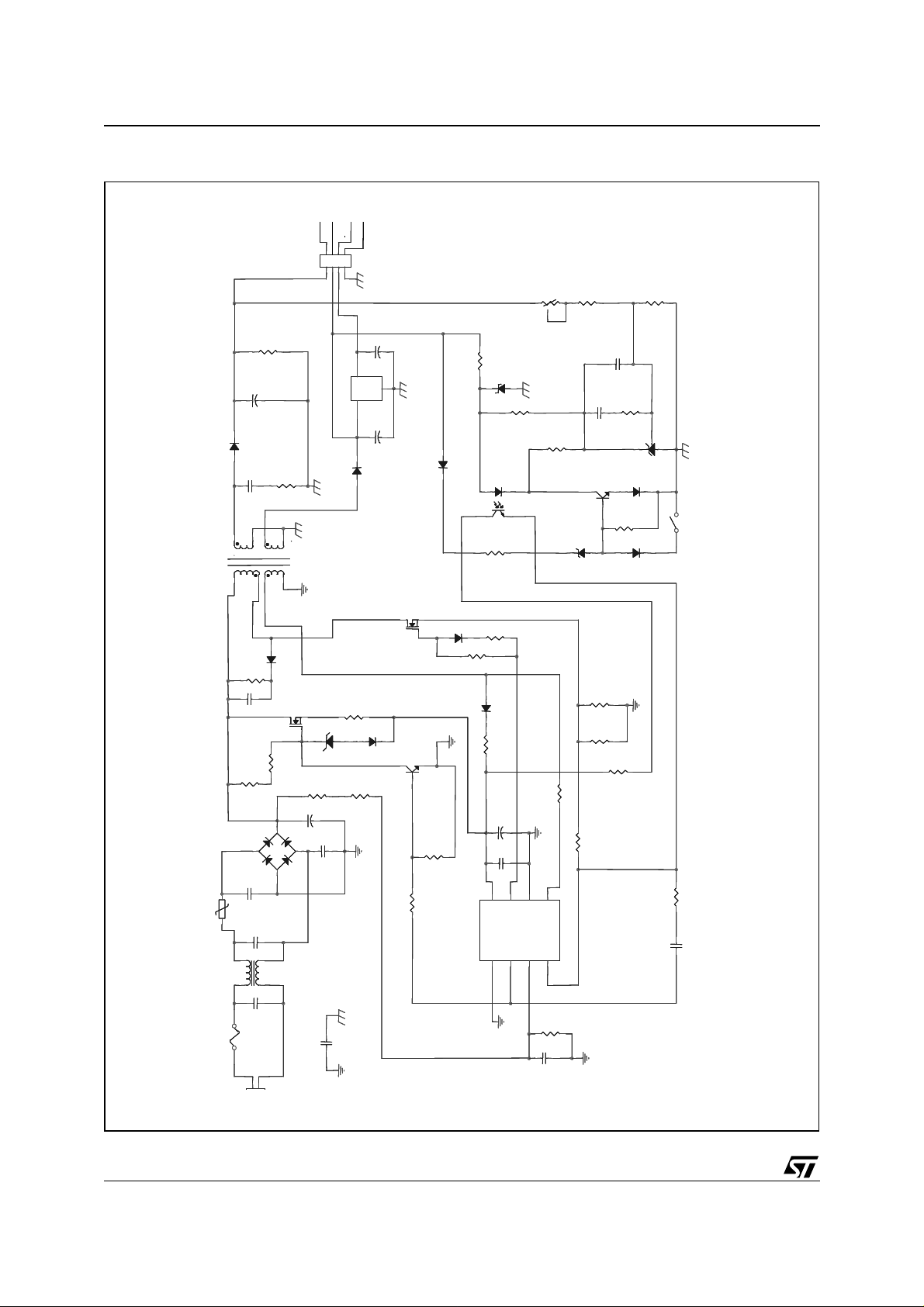
The complete schematic of the realized circuit is shown in figure 3. It is a two output switch mode power supply
with a third output for the micro controller, obtained through a voltage regul ator (LE50C), from the secondary
output (V
=14V). The electrical specification is listed in table 1:
out2
Table 1.
Input Voltage range 88 to 264 Vac
Mains frequency 50-60 Hz
Maximum output power 60 W
Output voltages Vout1 = 114V; Pout1 = 55 W
Vout2 = 14V; Pout2 = 4.2 W
Output of the voltage regulator Vout
Minimum switching frequency 70 kHz
Target efficiency η > 80%
Maximum standby consumption (@ 220 Vac) < 1W
=5V; Iout
3
= 70mA; Iout
wup
stand-by
=10mA
3/10
Page 4
AN1729 APPLICATION NOTE
n
m
n
m
Figure 3. Complete schematic of the 60W SMPS for 14" TV
Grou
Grou
14V 4.2
114V 555V 350
14V 4.2
114V 555V 350
J8
CON41234
J8
CON41234
J8
CON41234
114V 50W
114V 50W
114V 50W
T3
T3
T3
176
176
176
R15
R15
R15
82k 1/2W
82k 1/2W
82k 1/2W
C4
C4
C4
100uF 1 60V
100uF 1 60V
100uF 1 60V
D4 STTH1L06
D4 STTH1L06
D4 STTH1L06
R14
C7
R14
C7
R14
C7
220 pF630V
220 pF630V
220 pF630V
91411
8
91411
8
91411
8
3
3
3
14V 4.2W
14V 4.2W
14V 4.2W
820
820
C8
4.7u
C8
4.7u
C8
4.7u
13
13
13
U1
U1
U1
56
56
56
Trasformer
Trasformer
Trasformer
2
2
2
OUTIN
OUTIN
OUTIN
Grou nd
Grou nd
Grou nd
LE05/TO92
LE05/TO92
LE05/TO92
C9
C9
C9
4700uF 25V
4700uF 25V
4700uF 25V
D5 STTH102
D5 STTH102
D5 STTH102
820
R16
R16
R16
DZ2
DZ2
DZ2
BZX7 9C 10
BZX7 9C 10
BZX7 9C 10
R11
R11
R11
D7
1N4148
D7
1N4148
D7
1N4148
ISO1
PC817
ISO1
PC817
PC817
12
12
12
4
3
4
3
4
3
R21
220
R21 ISO1
R21
220
220
R17
82K
R17
82K
R17
82K
20k
20k
20k
trim117
trim117
trim117
C14
C14
C14
10k
10k
10k
R19
270
R19
270
R19
270
Q3
Q3
Q3
123
123
123
BC547
BC547
BC547
1 2
1 2
1 2
DZ3
DZ3
DZ3
BZX79C7V5
BZX79C7V5
BZX79C7V5
R20
2.2K
R20
2.2K
R20
2.2K
C13
180pF
C13
180pF
C13
180pF
3.3 nF
3.3 nF
3.3 nF
R18
220k
R18
220k
R18
220k
IC3
TL431
IC3
TL431
IC3
TL431
3
3
3
2 1
2 1
2 1
DIODE
DIODE
DIODE
D8
D8
D8
R22
180
R22
180
R22
180
SW1
SW1
SW1
1 2
1 2
1 2
D9
D9
D9
1N4148
1N4148
1N4148
Q2
STP7NC80Z
Q2
STP7NC80Z
Q2
STP7NC80Z
2
3
2
3
2
Drain
Drain
Drain
D1
D1
D1
R3
220k 1W
R3
220k 1W
R3
220k 1W
STTH 1L 06
STTH 1L 06
STTH 1L 06
C3
C3
C3
47nF 450V
47nF 450V
47nF 450V
Q5
Q5
Q5
2
3
2
3
2
3
1
1
1
RH1
4.7M
RH1
4.7M
RH1
4.7M
RH2 4.7M
RH2 4.7M
1nF 40 0V
1nF 40 0V
1nF 40 0V
3
3
3
Filtred_AC+
Filtred_AC+
Filtred_AC+
L1
L1
L1
4
4
4
AC_Main+
AC_Main+
AC_Main+
RH2 4.7M
4
4
4
BR1
BR1
BR1
3
3
3
STBR406
STBR406
STBR406
-+
-+
-+
1
1
1
CY1
CY1
CY1
CX2
CX2
CX2
100nF 450V
100nF 450V
100nF 450V
2
2
2
27mH
27mH
27mH
1
1
1
Cx1
Cx1
Cx1
100nF 450V
100nF 450V
100nF 450V
AC_Main-
AC_Main-
AC_Main-
Filtred_AC-
Filtred_AC-
Filtred_AC-
High_Voltage_Bus
High_Voltage_Bus
High_Voltage_Bus
Br in +
Br in +
Br in +
NTC1 22R
NTC1 22R
NTC1 22R
F1 FUSE
F1 FUSE
F1 FUSE
Auxiliar_Output
Auxiliar_Output
Auxiliar_Output
RH3
10 k
RH3
10 k
RH3
10 k
STQ1NC60
STQ1NC60
STQ1NC60
R1A
R1A
R1A
C1
C1
C1
150uF 450V
150uF 450V
150uF 450V
2
2
2
CY2
CY2
CY2
C17 2.2nF 2k V
C17 2.2nF 2k V
C17 2.2nF 2k V
D10
D11
15V
D10
D11
15V
D10
D11
15V
1 2
1 2
1 2
2.2M
2.2M
2.2M
R1B
2.2M
R1B
2.2M
R1B
2.2M
1nF 40 0V
1nF 40 0V
1nF 40 0V
3
R8
15
R8
15
R8
1
1
1
D3
D3
D3
1N4148
1N4148
1N4148
123
123
123
Q6
Q6
Q6
BC547
BC547
BC547
R23
22k
R23
22k
R23
22k
R24 100k
R24 100k
R24 100k
Vcomp_Pin
Vcomp_Pin
Vcomp_Pin
Voltage_Feed_Forward_Pin
Voltage_Feed_Forward_Pin
Voltage_ Fe ed_ Fo r ward _Pi n
15
1N4148
1N4148
1N4148
R7
100
R7
100
R7
100
D2
1N4148
D2
1N4148
D2
1N4148
Gate_Driver
Gate_Driver
Gate_Dri ver
R4 10
R4 10
R4 10
Vcc
Vcc
Vcc
C4A
22uF 25V
C4A
22uF 25V
C4A
22uF 25V
C4B
C4B
C4B
100nF (220 nF)
100nF (220 nF)
100nF (220 nF)
857
857
857
GD
GD
GD
Vcc
Vcc
Vcc
IC1
IC1
IC1
INV
Comp
INV
Comp
INV
Comp
1
2
3 6
1
2
3 6
1
2
3 6
Source
Source
Source
R10B
0.8 1/2W
R10B
0.8 1/2W
R10B
0.8 1/2W
R10A
0.8 1/2W
R10A
0.8 1/2W
R10A
0.8 1/2W
R26
3.3k
R26
3.3k
R26
3.3k
R5 47k
R5 47k
R5 47k
R9 680
R9 680
R9 680
Zero_Current_Detect
Zero_Current_Detect
Zero_Current_Detect
ZCD
ZCD
ZCD
L6565
L6565
L6565
VFF GND
CS
VFF GND
CS
VFF GND
CS
Current_Sense_Pin
Current_Sense_Pin
Current _Se nse _P in
4
4
4
R2
22k
R2
22k
R2
22k
1nF
1nF
1nF
C2
C2
C2
SW1 close - normal mode
SW1 open - stand-by mode
SW1 close - normal mode
SW1 open - stand-by mode
Instead of the Sw the microcontroller
control the stand-byfunction
Instead of the Sw the microcontroller
control the stand-byfunction
R25
5.6k
R25
5.6k
R25
5.6k
C16
0.56uF
C16
0.56uF
C16
0.56uF
4/10
Page 5

AN1729 APPLICATION NOTE
Enhanced Burst-Mode Operation
The start-up circuit plays an important role and it is important to look at its schematic redrawn in fig. 4.
The circuit is basically a current generator including a high-voltage MOS (Q5) that can be disabled through the
switch Q6 driven by the output of the error ampli f ier of t he L6565 (COMP). Note that the i nvert ing input of t he
error amplifier (INV) is connected to ground, while the non-inverting one is internally connected to a voltage reference of 2.5V. When the L6565 is on, the voltage on pin COMP (V
the controller is off, COMP is floa ting.
) is high (always > 2.5V) and, when
COMP
During the start-up phase the high voltage MOS is on and the current that charges the capacitor C4 on the V
pin flows through it. As soon as the L6565 is turned on, V
goes high, which turns on Q6 and, consequently,
COMP
CC
turns off Q5. Thus, the current flowing i n t he star t up network duri ng normal operation i s only t hat t hrough the
two resistors RH1 and RH2 (4.7M
Ω
each), therefore a really low power is dissipated (10 mW @ 220 Vac).
As previously said, the start-up circuit is arranged as a constant current generator, with the advantage of having
a start-up time of the converter independent of the mains voltage. The analytic expression of the current delivered by the generator is:
VzV
I
st up–
V
is the breakdown voltage of the Zener Diode DZ1, V
z
-------------------------------------------=
–+
DropVth
RH3
(Eq.1 )
is the voltage drop across D10 and Vth is the con-
Drop
duction threshold gate-source voltage of the MOS Q5 (STQ1NC60).
Figure 4. Sta rt up cir c ui t
Main s
R24 10 0K
R24 22K
Bulk
Capacitor
Q6
BC547
RH1
RH2
DZ1
D10
1N4148
Q5
STQ1NC60
RH3
comp
Pin8 V
CC
C4
Pin1 Inv
Pin2 V
L6565
In the circuit shown in the schematic of figure 3, the L6565 internal E/A is not used in the feedback loop. During
the normal operation of the converter his output (V
) is always at his maximum value of 5.8V. The feedback
COMP
loop is closed summing the feedback signal to the current sense signal through a resistor (R9 in the schematic)
between the current sense resistor and the current sense pin of the L6565. Thi s arrangement allows real izing
the enhanced burst-mode operation during standby through the circuit whose schematic is redrawn in figure 5.
If a large current is forced to flow in the resistance R9, the voltage on the current sense pin will exceed the second overcurrent protection threshold and this will disable the gate driver. To re-enable the driver, first the IC
must be turned off, that is the V
voltage must fall below the UVLO threshold.
CC
5/10
Page 6

AN1729 APPLICATION NOTE
When the micro controller of the TV gives the standby command, the switch SW1 is open and the 14V output
turns on the small signal bipolar transistor Q3. As a result, a big current (as compared to the current that flows
during normal operation) is forced to flow in the LED of the opto-coupler and thereby in both the phototransistor
and R9. As explained before, this big current will disable the gate driver of the L6565.
When the gate driver is disabled the quiescent current i s unchanged and, since no energy is coming from the
self-supply circuit, the V
the start-up generator will be enabled and a new start-up cycle will begin. The resulting behaviour will be a low
frequency intermittent operation that we will refer to as "enhanced burst-mode operation". With such operation
the regulation loop used in normal operation of the converter is skipped; another kind of regulation takes place.
The Secondary output of the converter starts to rise until it reaches a threshold V
DZ3 as V
+VBE+Vd where VBE is the base emitter voltage of the small signal transistor Q3 (BC547) and Vd
DZ3
is the voltage drop of the diode D8 (1N4148) (we can neglect the voltage drop on resistor R21). At this point the
gate driver of the controller is di sabled and switching is st opped. The length of this idl e period is fi xed by the
discharge time of the capacitor C4 as above explained. During this idle period the output voltages will go down
and the minimum values that they reach depends on their individual load.
In order to obtain some design equations we can divide the burst-mode period in three time intervals:
– Phase 1. From the moment when the L6565 controller has been just turned off and the start-up circuit
starts to re-charge the V
that is the V
– Phase 2. From when the L6565 is turned on until the transistor Q3 is turned on and the L6565 stops.
– Phase 3.From when the L656 5 stops to when the V
threshold and the L6565 is turned off.
capacitor (C4) will be discharged below the UVLO threshold after some time. Then
CC
fixed by the Zener diode
Omax
capacitor C4, to the moment when the controller is turned on,
CC
voltage exceeds the turn-on threshold.
CC
voltage goes down under the low UVLO
CC
Our purpose is to obtain simple equations, so some approximations will be introduced. An optimisation can be
done, looking at the measurement results, in order to have as good performance as possible.
– Phase 1.
After the VCC voltage has fallen below the UVLO off threshold, the start-up cycle begins. The high voltage low
current Mos Q5 is on and the capacitor C4 is charged through it and the resistor RH3. The starting value of the
voltage on C4 is the UVLO off threshold. The voltage value on C4 when the L6565 is turned on is t he turn-on
threshold. Their difference is the hysteresis V
of the capacitor C4 the charging time of C4 (T
T
ch C4–
V
th on–
------------------------------------------------------------- -
V
–()C4⋅
th off–
I
st up–
. Considering the equation 1 that gives the charging current
CCHys
) is the following:
ch-C4
Hys
V
Z
RH3 C4⋅⋅
–+
DropVth
(Eq. 2)
Vcc
------------------------------------------------- -==
V
– Phase 2.
When the L6565 is turned on the voltage on the secondary output is V
the output voltages rise. As soon Vout2 reaches the threshold V
DZ3
, the MOSFET starts switching and
Omin
+ V
+ Vd the BJT Q3 will be turned on
BE
and the gate driver of t he L6565 di sabled. The durati on of this switc hi ng phase i s t ypi call y much shorter than
the others and will be neglected.
– Phase 3.
The converter is stopped until the VCC voltage falls under the UVLO off thres hold. Let' s call Iq the quiescent
current of the L6565; the time for discharging the C4 capacitor is:
6/10
Page 7

AN1729 APPLICATION NOTE
T
disch C4–
Vcc
--------------------------------=
Hys
I
q
C4⋅
(Eq. 3 )
Summarizing, the total period of the enhanced burst-mode cycl e will be:
T
ch C4–
T
disch C4–
Vcc
------------------------------- -
⋅
HysC4
I
q
Vcc
Hys
------------------------------------------------- -+=+
V
z
RH3 C4⋅⋅
V
DropVth
Figure 5. Stand by Circuit
R10A//R10B
(Rsense)
R26
R9
Stand by
Circuit
DZ3
BZX79C7V5
R22
STTH102
R21
D8
D5
Q3
R19
TL1431
Secondary Output
C
9
R11
Compensation
network
–+
(Eq. 4)
Equivalent Load
LE50C
µC
R.C.
BZX79C10
How to set the timing of the enhanced burst-mode operation.
To have a well working circuit a minimum input voltage on the linear voltage regulator (V
) has to be guar-
OMin
anteed considering its dropout specification. We can summarize the power absorbed by the load (in thi s case
the micro controller, the LED, the receiver for the remote control of the TV and, of course, the power consumption of the voltage regulator) with a constant current source because of the linear voltage regulator.
The consumption of the micro controller that has to be considered in the design i s that feat ured between the
turn-on instant and the complete exit of the system from the standby condition.
This is due to the fact that if the TV is turned on at the beginning of the idle phase of the burst period, the discharge of the output capacitor will be faste r bec aus e th e mic ro is on and absorbs more current. We have to guarantee the correct voltage on the voltage regulator with the micro in on state until t he complete restart of the
converter. Let us call I
the total output current absorbed duri ng the stand by condition and I
stb
(wake up
Wup
current) the total output current at the turn on of the micro.
Most of the power in standby condition will be dissipated by the start up network and can be written as:
C4 Vcc
⋅⋅
PD
st up–
-------------------------------------------- -=
HysVin
T
burst
(Eq. 5)
7/10
Page 8

AN1729 APPLICATION NOTE
being Vin the DC voltage on the input bulk capacitor.
Switching losses, the power dissipated on the output rectifier diode, and the power dissipated in the input stage
are not easy to be evaluated analyti cally but they are anyway almost i ndependent from the burst period and
considerably lower than PD
Another quantity that can be evaluated is the power absorbed by the load:
P
Load
.
stup
V
OMaxVOmin stb–
----------------------------------------------------------------------- -=
+()I
2
⋅
stb
(Eq. 6)
V
Omin-stb
greater than V
in the valley voltage at the input of the linear regulator whil e this is absorbing I
, which corresponds to I
Omin
have a minimum possible value of T
calculated (P
Dstb
+ P
is 70% of the total power consumption i n st andby. Hence, c onsidering t he 1W con-
Load)
consumption. We can use the previous equations in order to
Wup
and, as a rule of thumb, we can assume that the power consumption
burst
and it is therefore
stb
sumption target, we have:
C4 Vcc
⋅⋅
T
burst
----------------------------------------------- -≥
700 mW P
From equation 5 we see that increasing T
sired, however there is a maximum limit to T
Considering that a minimum voltage on the input of the voltage regulator has to be guaranteed, T
to the maximum voltage that we have at the input of the voltage regulator V
HysVhV
–
Load
burst
burst
(Eq. 7 )
the power consumption in standby can be made as low as de-
.
is relate d
burst
(Fixed by the Zener diode DZ3)
OMax
and at the value of the output capacitor C9, according to the following equation:
T
⋅
burstIWup
V
Omax
V
in any case has to be lower then the output voltage of the converter during the normal operation; if it were
Omax
V
Omin
-------------------------------- -+=
C9
(Eq. 8)
not, the normal control loop would be activated and the behaviour of the converter would be different from what
is required. Fixing a low value for V
as it can be seen, it is not a big part of the total power consumption. At this point the value of T
values of C9 and V
is a trade-off between lowering the standby consumption and a not too big output ca-
OMax
means decreasing the power consumption of the voltage regulator but,
OMax
and then the
burst
pacitor.
Once fixed all the component values, the V
V
Ominstb
V
Omax
Omin-stb
can be calculated as:
T
⋅
burstIstb
-----------------------------–=
C9
(Eq. 9)
Standby calculations in the experimental board
In the board assembled for testing the standby function the Zener diode DZ3 has a Zener voltage of 7.5V.
It means that the V
from Eq. 8 the maximum T
T
BurstMax
value is about 7.5V+0.6V+0.6V=8.7V. The output Capacitor (C9) value is: 4700µF so
OMax
value has to be:
burst
V
--------------------------------------------------------------------------- -
–()C9 0.8⋅()⋅
OMaxVOMin
I
wupId
8.7V 5.5V–()
+
----------------------------------- - 3760 µF164ms=⋅==
70mA 3 mA+
where the tolerance of the electrolytic capacitor C9 (-20%) and the maximum quiescent current Id of the linear
voltage regulator has been considered.
The maximum discharge time of the capacitor C4 can be calculated as:
8/10
T
disch C4– Max–
---------------------------------------------
Vcc
Hys
I
qMin
C4 1.2⋅⋅
4.3 26.4µF⋅
------------------------------- - 71ms===
1.6mA
Page 9
AN1729 APPLICATION NOTE
The value of the capacitor C4 has been multiplied by 1.2 to account for its tolerance, the value of the quiescent
current is the minimum from the datasheet of the controller and also the maximum hysteresis of the on/off V
thresholds has been considered.
CC
The charge time of the capacitor C4 has to be less then T
erations and using eq. 2, a minimum I
, of 1.2 mA is needed. As a result, the values of 10kΩ, for the resis-
st-up
burstMax-Tdisch-C4-Ma x
. Following the previous consid-
tance RH3, and 15V, for the zener voltage of the zener diode DZ1, were chosen.
Experimental results
In this section the results of experimental tests on a board manufactured according to the schematic in figure 3
are reported. In table 2 the measured standby consumption at different values of the input voltage are shown:
Table 2. Standby Input Power Measurements
V
P
in-stand-by
in
88Vac 110Vac 220Vac 264Vac
320mW 390mW 682mW 83 5mW
Fig. 6 shows the measured waveforms of the output voltages and of the Voltage at the VCC pin.
Channel 1 is the output of the voltage regulator and i ts value is c onstant (~5V). Channel 2 is t he input of the
voltage regulator and here we can see that during the idle phase the voltage decreases linearly (the output capacitor is discharged with a constant current I
output voltage rises up from V
Ominstb
(Ch2Min = 7.48V) to V
), during the switching phase (note, it is actually very short) this
STB
(Ch2Max = 8.68V).
OMax
Figure 6. Standby waveforms: steady state with 10 mA load curr ent
Channel 3 shows the voltage on VCC pin of the controller L6565. As soon as this voltage reaches the UVLO onthreshold the system starts switching but, as soon as the voltage regulator input voltage reaches a value such
that the small signal bipolar Q3 is turned on, the gate driver of the L6565 is disabled, the switching is stopped
and the V
voltage decreases until the UVLO off-threshold. At this point the start-up network is on again and
CC
9/10
Page 10

AN1729 APPLICATION NOTE
the voltage on VCC pin starts rising.
In Fig. 7 the measured waveforms with 70mA load are shown. 70mA load is used to simulate the wake-up of
the micro controller. As can be seen, the voltage regulator input voltage (Ch2) minimum value (V
something more then the minimum voltage input for the LE50C Voltage regulator.
Figure 7. Standby waveforms: steady state with 70mA load cu rren t
OMin
) is 5.52V,
Conclusions
A low-cost solution for implementing an enhanced burst-mode operation, externally activated, that guarantees
a very low consumption in standby condition was proposed. It is based on a different but v ery simple strategy
of control that does not affect the behaviour of the circuit in normal operation. An analytic method to design the
standby circuit and estimate the power consumption of the converter in such condition was explained.
References
[1] "L6565 Quasi-Resonant Controller" (AN1326)
[2] L6565 datasheets
Information furnished is believed to be accurate and reliable. However, STMicroelectronics assumes no responsibility for the consequences
of use of such information nor for any infringement of patents or other rights of third parties which may result from its use. No license is granted
by implic ation or otherwise under any patent or patent r i ght s of STMi croelectr oni cs. Specifications menti oned in thi s publicati on are subj ect
to change without notice. This publication supersedes and replaces all information previously supplied. STMicroelectronics products are not
authorized for use as cri tical components in li f e support dev i ces or systems without express writ t en approval of STMicroel ectronics.
The ST logo is a registered trademark of STMicroelectronics
© 2003 STMic roelectroni cs - All Rig hts Reserved
Austra lia - Brazil - Canada - Ch i na - F i nl and - France - Germany - Hong Kong - India - Israel - Italy - Japan -Malay si a - Malta - Morocco -
Singap ore - Spain - Sw eden - Switzerland - Uni ted Kingdom - United St ates.
STMicroelectronics GROUP OF COMPANIES
http://www.s t. com
10/10
 Loading...