

Page 1
AN1725
APPLICATION NOTE
ADVANCED PERFORMANCE USING STG3699
M. Porto
1. ABSTRACT
IC analog switches t raditionally have found l imited use in applications involving high - freque ncy analog
or digital signals.
Degradation of switch performance and intolerable signal cross-talk between channels have undoubtedly
forced many microelectronics manu facturers to study new technologie s to solve the problem.
2. DEVICE DESCRIPTION
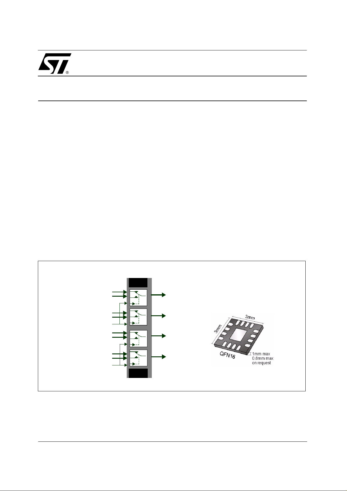
The STG3699 is a high speed CMOS with low on resistance and low voltage quad analog S.P.D.T.
(Single Pole Dual Throw) switch or quad 2:1 Multiplexer / Demultiplexer switch fabricat ed in C2MOS
technology.
These Analog Switches are designed to ope rate from 1.65V to 3.6V and offer asymmetrical normally
closed (NC) and normally open (NO) R
for applications that require asymmetrical loads (such as
ON
speaker headsets and internal speakers).
The STG369 9 has Brea k-Before-Make s witching and f ast swit ching features (t
= 2.7V).
at V
cc
ON
= t
= 30ns Typical
OFF
Figure 1: Quad Analog Switch
June 2003
1-2IN
3-4IN
1S1
1S2
2S1
2S2
3S1
3S2
4S1
4S2
VCC
GND
COM
COM
COM
COM
D1
D2
D3
D4
1/6
Page 2
AN1725 - APPLICATION NOTE
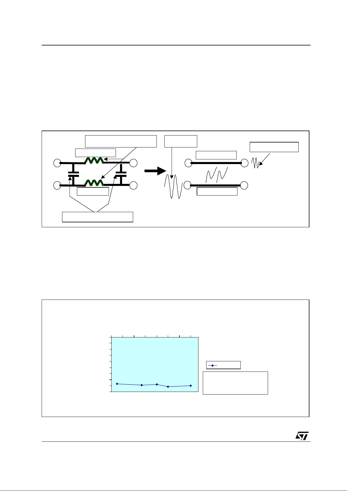
3. CROSS-TALK
The main sources of cross-talk are caused by parasitic line inductance generated by transmission line of
PCB and parasitic die capacitance generated by internal structure of the die.
The single channel cross-talk can be defined as the ratio between the unwanted signal present in a
channel switched ON, and the signal applied to another single Off channel input.
Figure2 shows the single channel cross-talk phenomenon.
Figure 2: Cross-Talk Phenomenon
Parasitic Line Inductance
Input Signal
Unwante d Signal
Channel OFF
Channel ON
Parasitic Die Capacitance
The value of cross talk are expressed in decibel by the following formula:
XTALK (dB) = 20log V
is the value of the unwanted signal present in the channel switche d ON, while Vin is the value of the
V
out
out
/ Vin
signal applied to the other single channel OFF input.
The internal architecture of the STG3699 device allows very low values of unwanted signal thus avoiding
interference between different signals applied on switch.
Figure 3: Cross-Talk
Cross - Tal k
Cross - Tal k
dB
dB
1.5 1.8 2.1 2.4 2.7 3 3.3 3.6
1.5 1.8 2.1 2.4 2.7 3 3.3 3.6
-20
-20
-25
-25
-30
-30
-35
-35
-40
-40
-45
-45
-50
-50
-55
-55
-60
-60
-65
-65
Vcc (V)
Vcc (V)
SSS Avg
SSS Avg
Temp. = 25°C
Temp. = 25°C
Vcc = from 1.65V to 3.6V
Vcc = from 1.65V to 3.6V
Corner = SSS
Corner = SSS
The previous chart shows the values (expressed in dB) of cross-talk depending on Power Supply.
2/6
Page 3

AN1725 - APPLICATION NOTE
4. CHARGE INJECTION
Charge injections con sist of the charge t ransferred from the digital driver to the analog chann el at the
time of switching the device to the "off" state (measured in pC). This unwanted charge is normally
induced through parasitic capacitance to source or gate to drain capacitance.
The table below shows the method to measure the charge injection.
Figure 4: Charge Injection Measurement Bench
The architecture of the internal circuitry of STG3 699 reduces this parasitic capacitance to a low value,
typically 200pC with Vcc range from 2.3V to 3.6V
The next formula shows how to calculate the value of charge injection:
Q = ∆V
OUT
x C
L
Note: where CL is the value of Load Capacitance
The chart below shows the variation of charge injection dep ending on Power Suppl y condition, using a
= 0.1nF and a ∆V
C
L
≅ 2mV
out
Figure 5: Charge Injection Characteristics
Charge injec tion Char ac teristic
Q (pC)
160
140
120
100
80
60
40
20
0
1.5 1.8 2.1 2.4 2.7 3 3.3 3.6
Vcc (V)
SSS Av g
3/6
Page 4

AN1725 - APPLICATION NOTE
5. TYPICAL APPLICATION FOR AUDIO APPLICATIONS
Before the STG369 9, realizing an application without interference from d ifferent loads was very hard,
because the coupling of several loa ds introduces noise proble ms, this caused the designer to study PC
boards that reduced noise at the cost of fewer features.
Figure 6: Previous Mobile Phone Application
BB
Chipset
3V
Receiver
Melody IC
5V
SPK+
SPK-
8Ω Speaker
Using the Analog Switch STG 3699, it is possible to drive s ome receiver without interferenc e. Thanks to
low cross-talk the typical value meas ured for these devices was -54dB at a Power Supply range from
1.65V to 3.6V.
Figure7: Typical Application Using the STG3699
The designer can realize a layout for a very complex PC board, using, for example, a sound amplifier for
the speaker and receiver to improve High Fidelity sound, and coupling a different load (EARJACK) without
interference among signals.
4/6
Page 5

6. FEATURES
The features of STG3699 are summarized in the table below:
Table 1: STG3699 Fea tures
Low Ron = 0.5 ohm Typ (3V Supply); 3 ohm Max (+1.8V Supply)
0 .15 ohm Max Ron Flatness (+ 2.7V Supply)
High-Curre nt Handing Capacity (150mA Continuous)
Low Cross-talk – 54dB Typ.
Available in TSSOP and QF N packages
Fast switching (300 ps typical TPD with Vcc = 3V)
High Electric Static D ischarge protection >3KV
1.65V to 3.6 V Single Supply V o ltage
AN1725 - APPLICATION NOTE
7. COMPATIBILITY OF STG3699 WITH COMPETITORS’ DEVICES
The pin configuration of Quad SPDT STG3699 is compatible with competitors’ MAX4699 while the
electrical characteristics are compatible with competitors’ Dual SPDT Max4684 Analog Switch.
The table below shows some common electrical parameters.
Table 2: Electrica l Parameters
STG3699 COMPETITOR
Cross–Talk = -54dB, Vcc from
1.65V to 3.6V
Cross–Talk = -54dB, Vcc from 2.7V
to 3.6V
QFN and TSSOP packages UCSP package
RON = 0.5Ω with Vcc = 2.7V RON = 0.5Ω with Vcc = 2.7V
RON flatness = 0.15Ω Vcc = 2.7V RON flatness = 0.15Ω Vcc = 2.7V
Vcc fr om 1.65 V to 3.6V Vcc from 1.8V to 5.5V
Vin < Vcc Vin < Vcc
ST’s portfolio also offers a 3V Dual SPDT Analog Switch named STG3684 with the same performance.
5/6
Page 6

AN1725 - APPLICATION NOTE
8. CONCLUSIONS
The Quad Anal og Switch STG 3699 allo ws several uses in different applicat ions where t he R
, Cross-
ON
Talk, Charge injection and the other features present in these devices are very important, as shown in
these pages. Thanks to the QFN package, these devices are suitable for applications where the small PC
board layout is basic, such as wire lines and telecom segments.
In fact, it is possible to realize a PCB using a single ST device instead of two Competitors’ devices.
Information furnished is believed to b e accurate an d reliable. How ever , STM icroelectronics assum es no resp onsibility
for the consequences of use of such information nor for any infringement of patents or other rights of third parties
which may result from its use. No license is granted by implication or otherwise under any patent or patent rights of
STMicroelectronics. Specification ment ioned in this p ublication are subject to change without notice. This publication
supersedes and repla ces all information previou sly supp lied. STM icro elect ronics pro ducts are not authorized for use
as critical components in life support devices or systems witho ut expres s written approva l of STMicroelect ro nics.
The ST logo is a registered trademark of STMicroelectronics
© 2003 STMicroelectronics - Printed in Italy - All rights reserved
STMicroelectronics GROUP OF COMPANIES
Australia - Brazil - Canada - China - Finland - France - Germ any - Hong Kon g - India - Isreal - Italy - Japan - Malaysia
- Malta - Morocco - Singapore - Spain - Sweden - Switzerland - United Kingdom - U.S.A.
http://www.st.com
6/6
 Loading...