

Page 1

AN1724
APPLICATION NOTE
Conversion Guide, uPSD3200 to uPSD3300 Series
Overview
The uPSD family currently consists of two series, uPSD3200 and uPSD3300. Both are available in the
same kind of packages, but there are a few differences in pin definitions. This document describes the
differences and suggests methods to easily migrate designs from the uPSD3200 series to uPSD3300.
You can implement simple techniques on your printed circuit board to accept either a uPSD3200 or a
uPSD3300 during manufacturing.
Pin differences will be presented two categories:
1. Mandatory pin function changes for all applications
2. Conditional pin function changes depending on the application.
There are also differences in SFRs and interrupt vectors, which may impact firmware depending on the
application. These differences are identified to help you migrate your firmware.
For simplicity, the uPSD3200 series will be referred in this document as 3200, and the Turbo uPSD3300
series will be referred to as 3300.
Rev 1
June 2005 1/24
www.st.com
24
Page 2

AN1724
Contents
1 Summary of Differences . . . . . . . . . . . . . . . . . . . . . . . . . . . . . . . . . . . . . . . . 3
2 Summary of new uPSD3300 functions . . . . . . . . . . . . . . . . . . . . . . . . . . . . 4
3 Pin Definitions . . . . . . . . . . . . . . . . . . . . . . . . . . . . . . . . . . . . . . . . . . . . . . . . 6
4 Mandatory PIN Changes . . . . . . . . . . . . . . . . . . . . . . . . . . . . . . . . . . . . . . . 10
4.1 52-pin Devices (see Figure 1 and 2) . . . . . . . . . . . . . . . . . . . . . . . . . . . . . . . 10
4.2 80-pin Devices (see Figure 3 and 4) . . . . . . . . . . . . . . . . . . . . . . . . . . . . . . . 10
4.3 PC Layout Suggestions . . . . . . . . . . . . . . . . . . . . . . . . . . . . . . . . . . . . . . . . . 11
5 Conditional PIN Changes . . . . . . . . . . . . . . . . . . . . . . . . . . . . . . . . . . . . . . 14
5.1 PWM . . . . . . . . . . . . . . . . . . . . . . . . . . . . . . . . . . . . . . . . . . . . . . . . . . . . . . . 14
5.1.1 52-pin Devices (see Figure 1 and 2) . . . . . . . . . . . . . . . . . . . . . . . . . . . . . . . 14
5.1.2 80-pin Devices (See Figure 3 and 4) . . . . . . . . . . . . . . . . . . . . . . . . . . . . . . . 14
5.1.3 PC Layout Suggestion for PWM . . . . . . . . . . . . . . . . . . . . . . . . . . . . . . . . . . 14
5.2 ADC . . . . . . . . . . . . . . . . . . . . . . . . . . . . . . . . . . . . . . . . . . . . . . . . . . . . . . . 15
5.2.1 Reassigned ADC Channel Numbers . . . . . . . . . . . . . . . . . . . . . . . . . . . . . . . 15
5.2.2 ADC Voltage Scaling . . . . . . . . . . . . . . . . . . . . . . . . . . . . . . . . . . . . . . . . . . . 15
5.2.3 ADC Reference Voltage . . . . . . . . . . . . . . . . . . . . . . . . . . . . . . . . . . . . . . . . 16
5.3 LVD . . . . . . . . . . . . . . . . . . . . . . . . . . . . . . . . . . . . . . . . . . . . . . . . . . . . . . . . 16
6 Special Function Register (SFR) Differences . . . . . . . . . . . . . . . . . . . . . . 18
7 Interrupt Vector Differences . . . . . . . . . . . . . . . . . . . . . . . . . . . . . . . . . . . . 20
8 Conclusion . . . . . . . . . . . . . . . . . . . . . . . . . . . . . . . . . . . . . . . . . . . . . . . . . . 21
9 Contact Information . . . . . . . . . . . . . . . . . . . . . . . . . . . . . . . . . . . . . . . . . . 22
10 Revision history . . . . . . . . . . . . . . . . . . . . . . . . . . . . . . . . . . . . . . . . . . . . . . 23
2/24
Page 3

AN1724 1 Summary of Differences
1 Summary of Differences
● MCU CORE VOLTAGE: The 3300 MCU core requires a 3.3V supply, even when used in a
5V system. This means two separate supplies (5V V
system, but just one supply (3.3V V
devices use only a single V
supply, which is 5V VCC for 5V devices, or 3.3V VCC for 3.3V
CC
) is required for a 3.3V system. In contrast, 3200
CC
devices.
● MCU CORE: The 3200 MCU requires 12 clocks per instruction but the 3300 uses just 4
clocks. The 3300 does not have an optional 12-clock operation mode. NO modifications
are needed to 3200 firmware for standard 8032 functions unless timing was established
with software loops. Modifications ARE required for firmware controlling some peripherals
when migrating to 3300.
● PWM: The five 8-bit PWM channels of the 3200 are implemented with the Programmable
Counter Array (PCA) in the 3300, which has six 16-bit timer/counter modules. There are
new SFRs, and some PWM pin number assignments have changed on the 3300.
● ADC: The four 8-bit ADC channels of the 3200 are implemented using four of the eight 10-
bit ADC channels on the 3300. There are new SFRs, but there are no ADC input pin
number changes. The ADC reference voltage (V
3300 devices and V
devices do have an ADC V
voltage on any 3300 ADC input is V
LV D: Both 5V and 3.3V 3300 devices have Low-Voltage Detect (LVD) trip point set for the
●
3.3V V
● WATCHDOG: The watchdog timer is enabled after reset on 3200 devices, but it is disabled
supply level (2.5V). This must be considered when designing 5V system.
CC
is shared internally with the 3.3V VCC core supply. 80-pin 3300
REF
pin, and its max input voltage is V
REF
(3.3V) even in a 5V system
CC
after reset on 3300 devices.
● I/O Characteristics: The 3.3V 3300 devices have 5V tolerant I/O on ports 1, 3, and 4, but
ports A,B,C, and D are not 5V tolerant. The 3.3V 3200 devices do not have any 5V tolerant
I/O.
● UART and I
● USB and DDC: No USB or DDC interfaces are on the 3300.
2
C: Minor changes to SFR definitions.
and 3.3V VCC) are required in a 5V
DD
) input pin is not available on 52-pin
REF
(3.3V). The max input
CC
.
3/24
Page 4

2 Summary of new uPSD3300 functions AN1724
2 Summary of new uPSD3300 functions
Listed below are new functions on the 3300 that were not available on the 3200. Obviously
there is no direct migration path for these new functions since the 3200 does not have them.
However, you should be aware of the new functions so you can plan to take advantage of them.
● SPI: An SPI bus master interface is provided on the 3300.
● ADC: Eight 10-bit ADC inputs are provided, compared to only four 8-bit ADC inputs on the
3200.
● IrDA: The 2
transceiver.
● PCA: The Programmable Counter Array unit has six 16-bit timer/counter (TC) modules
that can be used for PWM, Capture/Compare, Timers, or Counters. Three of the six TC
modules can operate from one time base, and the other three TC modules can operate
from another time base if desired. These six TC modules are in addition to the standard
three 16-bit timer units inside the 8032 MCU core, bringing a total of nine 16-bit timer/
counters. The 3200 provides only the three standard 16-bit 8032 timers.
● MCU Core: The 3300 Turbo MCU core has a six-deep instruction prefetch queue and a
four-way branching address cache to increase performance. Code in smaller localities
operate very fast. No special firmware is required to take advantage of the prefetch queue
or branching cache, other than writing to an SFR to enable these features. Be aware that
firmware timing loops will not be accurate because of the non-deterministic nature of
pipeline and cache architecture. Please use one of the many hardware timer modules to
create timing functions, not firmware loops.
● MCU Core: The 3300 Turbo MCU core includes dual data pointers to speed data transfers
of XDATA. The pointers can auto-increment and auto-decrement, providing rapid data
movement from source to destination locations. The 3200 has one only data pointer.
● JTAG Debug: The JTAG port now functions as a debug port in addition to In-System
Programming (ISP). This eliminates the need for conventional hardware In-Circuit
Emulation (ICE) tools.
● Debug: The 3300 has a dedicated debug input/output pin. As an output, it can signal that
a specified debug event has occurred, as an input it can trigger a debug event to begin
(breakpoint, trace, and so forth).
● MCU Clock: 3.3V 3300 devices can be clocked up to 40MHz, unlike 3.3V 3200 with
24MHz max.
● MCU Clock: 8032 MCU clock can be divided internally for lower power operation. The
MCU may change the clock divider ratio on-the-fly using SFRs. This affects the MCU only,
not peripheral clocks.
● Cross-Bar I/O: Peripheral functions on Port 1 are also available on Port 4 (cross-bar
switch), providing more flexibility. There is no need to sacrifice one peripheral function
when two functions are available on a single pin, just use the other port.
● High Current I/O: Eight I/O pins on Port 4 are each capable of sinking or sourcing 10mA,
for both 3.3V and 5.0V 3300. In contrast, 3.3V 3200 pins are capable of sinking 4mA each,
5V 3200 sink 8mA each.
● 5V Tolerant I/O: The following pins are 5V tolerant on 3.3V, 52-pin 3300 devices: P1.1
through P1.7, P3.1 through P3.7, P4.1 through P4.7, and RESET_IN_. On 3.3V, 80-pin
3300 devices, the following pins are also 5V tolerant: MCU_AD0 through MCU_AD7,
nd
UART channel supports IrDA protocol, which be connected directly to an IR
4/24
Page 5

AN1724 2 Summary of new uPSD3300 functions
MCU_A8 through MCU_A11, RD_, WR_, and _PSEN. In contrast, 3.3V 3200 devices had
no 5V tolerant I/O pins.
Note: Note: The PSD functions have NOT changed at all from 3200 to 3300. These functions include
PLD, memory mapping, memory management (code space vs. data space, and paging), Flash
memories, SRAM memory, PSD I/O. All changes in the 3300 are related to the MCU and not
the PSD.
5/24
Page 6
3 Pin Definitions AN1724
3 Pin Definitions
Figure 1, Figure 2., Figure 3., and Figure 4. show pin assignments of the 3200 and 3300
devices in both 52-pin and 80-pin TQFP packages. Please see the 3200 and 3300 data sheets
for detailed pin function descriptions and physical dimensions of packages. Pins requiring
mandatory changes during migration are darkened in the figures.
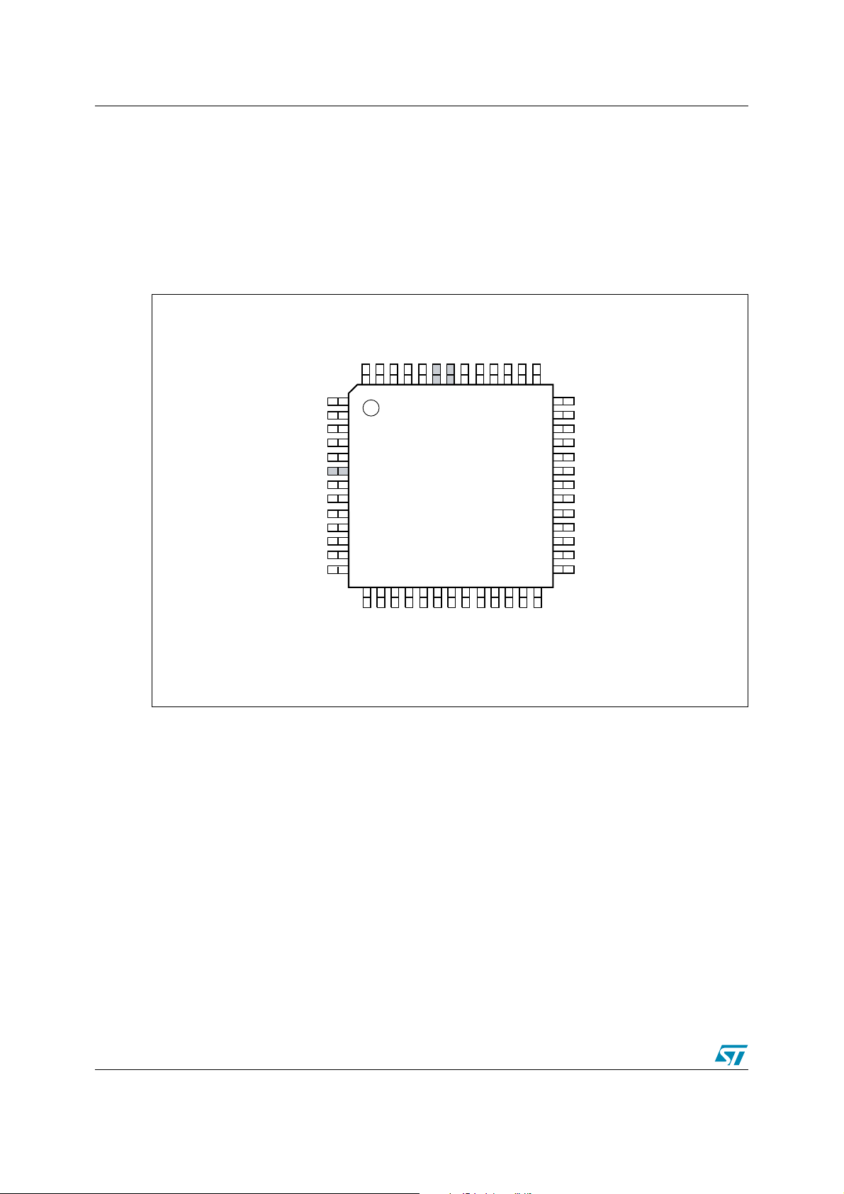
Figure 1. uPSD3200 52-pin TQFP Pin Definition
REF
GND
RESET_
PB6
PB7
P1.7/ADC3
PB0
PB1
PB2
PB3
PB4
PB5
V
52515049484746454443424140
P1.6/ADC2
PD1/CLKIN
PC7
JTAG TDO
JTAG TDI
USB–
PC4/TERR_
USB+
V
GND
PC3/TSTAT
PC2/V
STBY
JTAG TCK
JTAG TMS
1
2
3
4
5
6
7
8
CC
9
10
11
12
13
14151617181920212223242526
P4.7 / PWM4
52-pin TQFP
P4.6 / PWM3
P4.5 / PWM2
P4.4 / PWM1
uPSD32XX
GND
SYNC
P4.3 / PWM0
P4.2/DDC V
P3.1 / TXD
P3.0 / RXD
P4.1/DDC SCL
P4.0/DDC SDA
P3.2 / EXINT0
39 P1.5 / ADC1
38 P1.4 / ADC0
37 P1.3 / TXD1
36 P1.2 / RXD1
35 P1.1 / T2X
34 P1.0 / T2
33 V
32 XTAL2
31 XTAL1
30 P3.7 / SCL1
29 P3.6 / SDA1
28 P3.5 / T1
27 P3.4 / T0
P3.3 / EXINT1
CC
AI08812
6/24
Page 7
AN1724 3 Pin Definitions
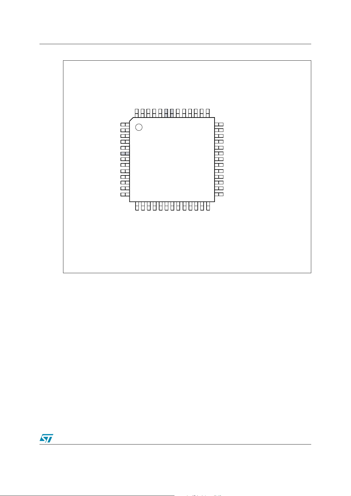
Figure 2. uPSD3300 52-pin TQFP Pin Definition
/ADC7
(3)
REF
/V
CC
PB5
GND
RESET_IN_
PB0
PB1
PB2
PB3
PB4
3.3V V
52515049484746454443424140
PB6
/ADC6
(2)
(2)
PB7
P1.7/SPISEL_
P1.6/SPITXD
(1)
(2)
2
CSCL
2
CSDA
(2)
/ADC1
/ADC0
AI08813
(2)
(2)
/ADC5
/ADC4
(2)
(2)
/ADC3
/ADC2
DEBUG
3.3V V
V
PC7
DD
GND
STBY
1
2
3
4
5
6
CC
7
(1)
8
9
10
11
12
13
PD1/CLKIN
JTAG TDO
JTAG TDI
PC4/TERR_
PC3/TSTAT
PC2/V
JTAG TCK
JTAG TMS
Note: 1 For 5V applications, V
39 P1.5/SPIRXD
38 P1.4/SPICLK
37 P1.3/TXD1(IrDA)
36 P1.2/RXD1(IrDA)
35 P1.1/T2X
uPSD33XX
52-pin TQFP
14151617181920212223242526
GND
TXD0/P3.1
/TCM4/P4.5
/TCM5/P4.6
/TCM3/P4.4
(2)
(2)
(2)
/PCACLK1/P4.7
(2)
SPICLK
SPITXD
SPIRXD
SPISEL_
must be connected to 5.0V source. For 3.3V applications, VDD must
DD
/TCM2/P4.2
(2)
/PCACLK0/P4.3
(2)
RXD1(IrDA)
TXD1(IrDA)
RXD0/P3.0
/TCM1/P4.1
/TCM0/P4.0
(2)
(2)
T2
T2X
EXTINT0/TG0/P3.2
34 P1.0/T2
33 V
DD
32 XTAL2
31 XTAL1
30 P3.7/I
29 P3.6/I
28 P3.5/C1
27 P3.4/C0
EXTINT1/TG1/P3.3
be connected to 3.3V source.
2 These signals can be used on one of two different ports (Port 1 or Port 4) for flexibility. Default is
Por t 1.
3V
and 3.3V VCC are shared. ADC channels must use 3.3V as V
REF
for 52-pin package.
REF
7/24
Page 8
3 Pin Definitions AN1724
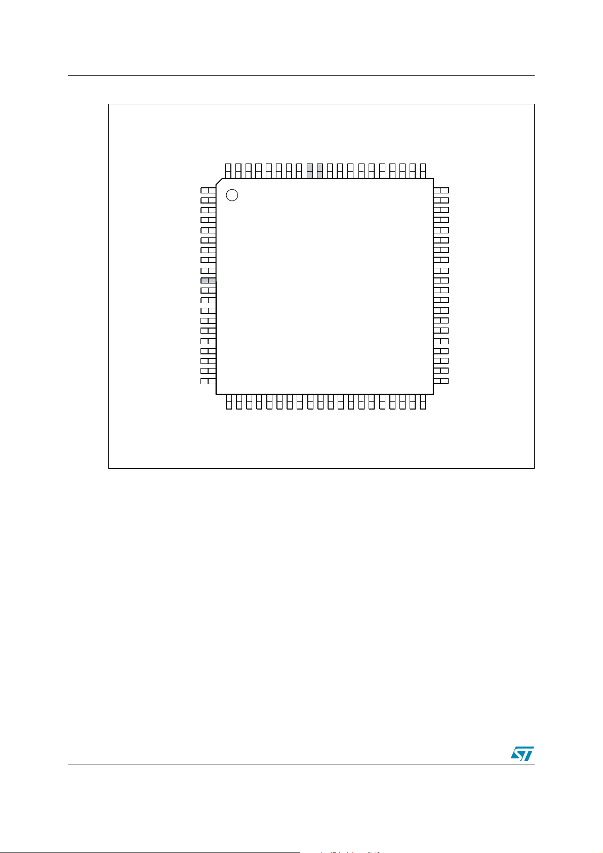
Figure 3. uPSD3200 80-pin TQFP Pin Definition
REF
GND
RESET_
PB6
PB7
RD_
P1.7 / ADC3
PSEN_
WR_
P1.6 / ADC2
61
60 P1.5 / ADC1
59 P1.4 / ADC0
58 P1.3 / TXD1
57 P2.3, A11
56 P1.2 / RXD1
55 P2.2, A10
54 P1.1 / T2X
53 P2.1, A9
52 P1.0 / T2
51 P2.0, A8
50 V
CC
49 XTAL2
48 XTAL1
47 P0.7, AD7
46 P3.7 / SCL1
45 P0.6, AD6
44 P3.6 / SDA1
43 P0.5, AD5
42 P3.5 / T1
41 P0.4, AD4
PD2
P3.3 /EXINT1
PD1
ALE
PC7
JTAG TDO
JTAG TDI
USB–
PC4/TERR_
USB+
NC
V
GND
PC3/TSTAT
PC2/V
STBY
JTAG TCK
NC
P4.7 / PWM4
P4.6 / PWM3
JTAG TMS
PB0
P3.2 / EXINT0
PB1
P3.1 / TXD
PB2
P3.0 / RXD
PB3
PB4
PB5NCV
80797877767574737271706968676665646362
1
2
3
4
5
6
7
8
9
10
11
12
CC
13
14
15
16
17
18
19
20
uPSD32XX
80-pin TQFP
21222324252627282930313233343536373839
PA7
PA6
PA5
PA4
P4.5 / PWM2
P4.4 / PWM1
PA3
GND
P4.3 / PWM0
P4.2
P4.1
PA2
P4.0
PA1
PA0
AD0, P0.0
AD1, P0.1
AD2, P0.2
40
P3.4 / T0
AD3, P0.3
AI08814
8/24
Page 9

AN1724 3 Pin Definitions
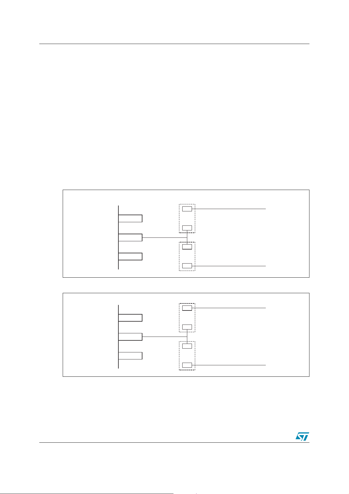
Figure 4. uPSD3300 80-pin TQFP Pin Definition
/ADC7
/ADC6
(2)
(2)
CC
PB0
P3.2/EXINT0/TG0
PB1
P3.1/TXD0
PB2
P3.0/RXD0
80797877767574737271706968676665646362
PB3
PB4
3.3V V
PB5
REF
V
GND
RESET_IN_
PB6
PB7
RD_
P1.7/SPISEL_
PSEN_
WR_
P1.6/SPITXD
61
SPISEL_
SPITXD
P3.3/TG1/EXINT1
(2)
PD2
PD1
ALE
PC7
JTAG TDO
JTAG TDI
DEBUG
PC4/TERR_
3.3V V
V
DD
GND
PC3/TSTAT
PC2/V
STBY
JTAG TCK
/PCACLK1/P4.7
(2)
/TCM5/P4.6
JTAG TMS
1
2
3
4
5
6
7
8
9
10
CC
NC
11
(1)
12
13
14
15
16
NC
17
18
19
20
21222324252627282930313233343536373839
PA7
PA6
PA5
/TCM4/P4.5
(2)
SPIRXD
PA4
/TCM3/P4.4
(2)
(2)
SPICLK
uPSD33XX
80-pin TQFP
PA3
GND
/TCM2/P4.2
(2)
/PCACLK0/P4.3
RXD1(IrDA)
TXD1(IrDA)
PA2
/TCM1/P4.1
(2)
T2X
PA1
/TCM0/P4.0
(2)
T2
PA0
MCU AD0
MCU AD1
MCU AD2
MCU AD3
60 P1.5/SPIRXD
59 P1.4/SPICLK
58 P1.3/TXD1(IrDA)
57 MCU A11
56 P1.2/RXD1(IrDA)
55 MCU A10
54 P1.1/T2X
53 MCU A9
52 P1.0/T2
51 MCU A8
50 V
49 XTAL2
48 XTAL1
47 MCU AD7
46 P3.7/I
45 MCU AD6
44 P3.6/I
43 MCU AD5
42 P3.5/C1
41 MCU AD4
40
P3.4/C0
(2)
/ADC5
(2)
/ADC4
(2)
/ADC3
(2)
/ADC2
(2)
/ADC1
(2)
/ADC0
(1)
DD
2
CSCL
2
CSDA
AI08815
Note: 1 For 5V applications, V
must be connected to 5.0V source. For 3.3V applications, VDD must
DD
be connected to 3.3V source.
2 These signals can be used on one of two different ports (Port 1 or Port 4) for flexibility. Default is
Por t 1.
9/24
Page 10

4 Mandatory PIN Changes AN1724
4 Mandatory PIN Changes
There are some pin changes that are absolutely required when migrating from the 3200. These
changes are a result of the additional voltage source required by the 3300 MCU core, and are
highlighted as dark colored pins in Figure 1, Figure 2., Figure 3., and Figure 4. above.
4.1 52-pin Devices (see Figure 1 and Figure 2.)
● Pins 46 and 47
– The function of pins 46 and 47 have swapped. The signal PB5 was on pin 47 for the
3200, but now is on pin 46 for the 3300. Pin 47 on the 3300 must always be
connected to 3.3V V
–The ADC V
(voltage reference) input was on pin 46 for the 3200, but is now on pin
REF
47 for the 3300.
–V
on pin 47 of the 3300 is shared internally with 3.3V VCC for either 3.3V and 5V
REF
3300 devices. This means no external ADC voltage reference is available, and ADC
signal inputs should be scaled to 3.3V V
a 5V 3300 device.
● Pins 6 and 7
– The function of pin 6 (PC4) on 3200 devices has moved to pin 7 on the 3300.
– The function of Pin 7 (USB+) on 3200 devices is not needed on the 3300 since USB
is not available.
– Pin 6 on the 3300 is now V
● Pin 5
– Pin 5 (USB-) on the 3200 must be pulled up to V
The pull-up resistor value for 3.3V 3200 devices is 2KΩ, the pull-up value for 5V 3200
devices is 7.5KΩ.
– The function of pin 5 (USB-) on 3200 devices is not needed on the 3300 since USB is
not available.
– Pin 5 on 3300 devices now functions as a Debug input/output, and does not need a
● V
pull up to V
and V
CC
DD
CC
.
– In a 3.3V system using a 3.3V 3300 device, pins 6, 8, 33, 47 must be connected to a
3.3V V
source.
CC
– In a 5V system, using a 5V 3300 device, pins 6 and 47 should be connected to a 3.3V
V
source, and pins 8 and 33 should be connected to a 5.0V VDD source.
CC
supply.
CC
for their maximum range, even when using
CC
and must always be connected to a 3.3V VCC supply.
CC
, regardless if USB is used or not.
CC
4.2 80-pin Devices (see Figure 3 and Figure 4.)
● Pins 71 and 72
– The function of pins 71 and 72 have swapped. The signal PB5 was on pin 72 for the
3200, but now is on pin 71 for the 3300. Pin 72 on the 3300 must always be
connected to 3.3V V
10/24
supply.
CC
Page 11

AN1724 4 Mandatory PIN Changes
● Pin 10
– Pin 10 is the USB+ signal on 3200 devices equipped with USB. Ideally, this pin was
not connected to anything before migrating to 3300. USB is not available on the 3300.
– Pin 10 must always be connected to 3.3V V
● Pin 8
– Pin 8 (USB-) on the 3200 must be pulled up to V
The pull-up resistor value for 3.3V 3200 devices is 2KΩ, the pull-up value for 5V 3200
devices is 7.5KΩ.
– The function of pin 8 (USB-) on 3200 devices is not needed on the 3300 since USB is
not available.
– Pin 8 on 3300 devices now functions as a Debug input/output, and does not need a
● V
pull up to V
and V
CC
DD
CC
.
– In a 3.3V system using a 3.3V 3300 device, pins 10, 12, 50, 72 must connect to 3.3V
V
source.
CC
– In a 5V system, using a 5V 3300 device, pins 10 and 72 should be connected to a
3.3V V
source, and pins 12 and 50 should be connected to a 5.0V VDD source.
CC
on the 3300.
CC
, regardless if USB is used or not.
CC
4.3 PC Layout Suggestions
You can plan your printed circuit board layout in anticipation of migrating from the 3200 to the
3300 by using simple and low cost techniques. One method involves the use of zero ohm (0Ω)
resistors (either surface-mount or thru-hole) and multiple circuit traces on the printed circuit
board. The idea is to install or not install these 0Ω resistors at the time of board manufacture
depending on which uPSD is installed.
For example, Figure 5 shows how you can use this method to handle the swapped functions of
pins 46 and 47 on the 52-pin uPSD. If a 3200 device is installed, resistor positions R1, R4, and
R6 would be populated with 0Ω resistors during manufacturing while leaving R2, R3, and R5
blank. If a 3300 devices is installed, resistors R2, R3, and R5 are populated and R2, R4, and
R6 are blank. A similar method can be used for an 80-pin device, using pins 71 and 72 instead
of pins 46 and 47, respectively.
Figure 6 illustrates one way to handle the differing functions of pins 6 and 7 on the 52-pin
uPSD. Pin 7 is USB+ on some 3200 devices, and it is assumed USB is not used in the 3200
application, meaning pin 7 was not connected to anything prior to migration to 3300. For this
example, when a 3300 device is installed during manufacturing, a 0Ω resistor is installed at
positions R1 and R3, leaving R2 blank. When a 3200 is installed, R2 gets a 0Ω resistor and R1
and R3 are blank. For 80-pin uPSDs, the signal PC4 does not change pin numbers when
migrating from 3200 to 3300 devices, so a simpler method is shown in Figure 7. When an 80-
pin 3300 device is installed, R1 is populated, but RI is blank when an 80-pin 3200 is installed.
11/24
Page 12

4 Mandatory PIN Changes AN1724
Figure 5. PC Layout Example for Pin Swapping
R1
uPSD
(52-pin)
Pin 47
Pin 46
Figure 6. PC Layout Example for V
uPSD
(52-pin)
Pin 7
Pin 6
R2
R3
R4
on 52-pin Devices
CC
R1
R2
R3
R5
R6
PB5
3.3V V
V
REF
AI08816
PC4
3.3V V
AI08817
CC
CC
Figure 7. PC Layout Example for V
uPSD
(80-pin)
Pin 10
on 80-pin Devices
CC
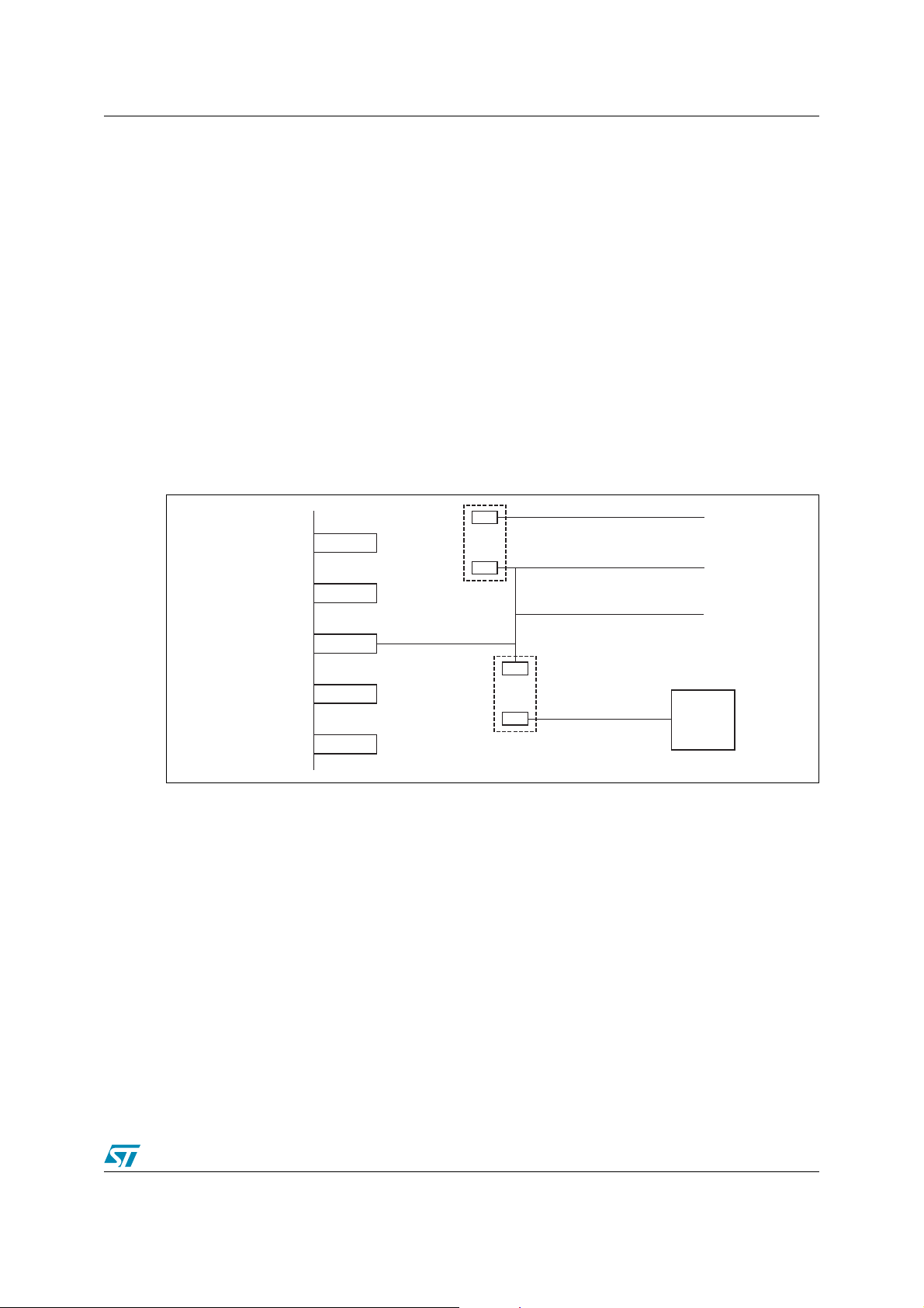
Figure 8 illustrates one way to handle the Debug signal on pin 5 of 52-pin 3300 device. There is
a conflict here because it is required to have a pull-up resistor on pin 5 of the 3200 (7.5KΩ on
5V 3200 devices, or 2KΩ on 3.3V 3200 devices), but pin 5 should have no pull-up on 3300
applications. A simple method using a 0Ω resistor is shown. When a 3200 device is installed,
R1 is populated with the appropriate pull-up resistor during manufacturing. When a 3300 device
is installed, R1 is blank. A similar method can be used for an 80-pin device using pin 8 instead
of pin 5.
The Debug signal is only for laboratory use and typically will be routed to a test point on the
circuit board.
12/24
R1
3.3V V
AI08818
CC
Page 13

AN1724 4 Mandatory PIN Changes
Figure 8. PC Layout Example for Debug Pin
uPSD
(52-pin)
Pin 5
R1
3.3V V
5.0V V
or
CC
for 3200
Debug
for 3300
AI08819
CC
13/24
Page 14

5 Conditional PIN Changes AN1724
5 Conditional PIN Changes
There are some pin changes that may or may not apply to your design, depending on your
application. These changes must be considered when migrating to the 3300 and you have used
the PWM or ADC peripherals of the 3200. There is also a conditional change regarding the use
of the Low-Voltage Detect (LVD) feature in 5V 3300 devices.
5.1 PWM
There are five PWM outputs on the 3200, and six PWM outputs on the 3300. If you have used
any of PWM outputs PWM1, PWM2, or PWM3, on the 3200 then there are no pin changes
when migrating to the 3300. However, if you have used PWM outputs PWM0 or PWM4 on the
3200, then you will have to connect to different pins on the 3300.
The Programmable Counter Array (PCA) on the 3300 has six Timer/Counter I/O pins, labeled
TCM0 through TCM5, that can be used for PWM outputs, and the PCA also has two clock input
pins labeled PCACLK0 and PCACLK1. These eight PCA pins are all on Port 4. It is the two
PCA clock input pins of the 3300 that conflict with the PWM0 and PMW4 pin assignments of the
3200.
5.1.1 52-pin Devices (see Figure 1 and Figure 2.)
If you are using up to three of the five PWM outputs on the 3200, do not use outputs PMW0 or
PWM4, instead use outputs PWM1, PWM2, or PWM3 and there will be no pin conflicts when
migrating to the 3300.
If you are using four or more PWM outputs on the 3200, then PWM0 on pin 18, or PWM4 on pin
14, will have to be moved to one of the one of following pins on the 3300: pins 15, 16, 17, 20,
21, or 22.
5.1.2 80-pin Devices (See Figure 3 and Figure 4.)
If you are using up to three of the five PWM outputs on the 3200, do not use outputs PMW0 or
PWM4, instead use outputs PWM1, PWM2, or PWM3 and there will be no pin conflicts when
migrating to the 3300.
If you are using four or more PWM outputs on the 3200, then PWM0 on pin 27 or PWM4 on pin
18 will have to be moved to one of the one of following pins on the 3300: pins 19, 23, 25, 30, 31,
or 33.
5.1.3 PC Layout Suggestion for PWM
Figure 9 is an example of how to move PWM output PWM0 on a 3200 device to PCA output
TCM2 on a 3300 device (52-pin). When a 3200 is installed, R1 is populated with a 0Ω resistor
and R2 is blank. When a 3300 is installed, only R2 is populated. A similar method can be used
for an 80-pin device using pins 27 and 30 instead of pins 18 and 20 respectively.
14/24
Page 15

AN1724 5 Conditional PIN Changes
Figure 9. PC Layout Example to Swap PWM Outputs
uPSD
(52-pin)
Pin 20
Pin 18
5.2 ADC
5.2.1 Reassigned ADC Channel Numbers
The 3200 has four ADC inputs (8-bit resolution), and the 3300 has eight ADC inputs (10-bit
resolution). The physical ADC input pin number numbers have not been changed, but the
logical ADC channel numbers change when migrating from 3200 to 3300. This means no
changes to PC board are required, but MCU firmware must change to account for different
channel numbers. Firmware changes must occur anyway because there are SFR changes,
identified in the next section. Ta bl e 1 refers to 52-pin uPSD devices, Ta bl e 2 refers to 80-pin
uPSD devices.
Table 1. Reassigned ADC Channel Numbers, 52-pin uPSD
Pin # on 52-pin TQFP 3200 Device 3300 Device
R2
R1
PWM_out
AI08820
38 ADC Channel 0 ADC Channel 4
39 ADC Channel 1 ADC Channel 5
40 ADC Channel 2 ADC Channel 6
41 ADC Channel 3 ADC Channel 7
Table 2. Reassigned ADC Channel Numbers, 80-pin uPSD
Pin # on 80-pin TQFP 3200 Device 3300 Device
59 ADC Channel 0 ADC Channel 4
60 ADC Channel 1 ADC Channel 5
61 ADC Channel 2 ADC Channel 6
64 ADC Channel 3 ADC Channel 7
5.2.2 ADC Voltage Scaling
For all 3300 devices, both 3.3V and 5V, the maximum input voltage level on any of the eight
ADC inputs is the MCU core voltage, V
be sampled in a 5V 3300 system, they must be scaled down to 3.3V V
(3.6V maximum). This means that if 5V signals are to
CC
15/24
. In contrast, for 5V
CC
Page 16
5 Conditional PIN Changes AN1724
3200 devices, if 5V signals are sampled, they do not have to be scaled down because the max
ADC input voltage is 5V V
(5.5V max).
CC
Figure 10 illustrates one way to scale a 0-5V analog signal down to 0-3.3V when a 3300 device
is used. For example, if a 3300 device is installed, resistor R1 is populated with a 332KΩ
resistor, and R2 is populated with a 665KΩ resistor. Precision 1% resistors are recommended.
Alternately, if a 3200 is installed, R1 is populated with a 0Ω resistor and R2 is left blank
because no scaling is needed.
5.2.3 ADC Reference Voltage
The maximum ADC reference voltage (V
V
(3.6V max), for both 3.3V and 5V 3300 devices. In contrast, for 5V 3200 devices the
CC
maximum ADC reference voltage is 5V V
the source for V
during manufacturing if needed. If a 5V 3200 is installed, R1 populated with
REF
) allowed on the 3300 is the MCU core voltage,
REF
(5.5V max). Figure 11 shows one method to switch
CC
a 0Ω resistor and R2 is blank. If a 5V 3300 is installed, only R2 gets the 0Ω resistor. This ONLY
applies to 80-pin uPSD devices, because 52-pin 3300 devices do not have a V
input as
REF
discussed in the mandatory pin change section above and Figure 5.
Figure 10. Scaling 5V Signal for 3.3V ADC Input
ANALOG
INPUT,
0 - 5V Range
uPSD
ADC Input
Figure 11. Switching Sources of V
R1
R2
in 80-pin uPSD Devices
REF
GND
AI08821
5.0V V
for 3200
CC
uPSD
(80-pin)
Pin 70
ADC V
REF
R1
R2
5.3 LVD
The Low Voltage Detect (LVD) circuitry on all 3300 (both 3.3V and 5V devices) will generate an
internal reset signal whenever the MCU 3.3V V
16/24
3.3V V
CC
for 3300
AI08822
voltage level dips below 2.5V. This is fine for
CC
Page 17
AN1724 5 Conditional PIN Changes
3.3V systems using a 3.3V 3300 device. However, for 5V systems using a 5V 3300 device, it is
recommended to use an external LVD circuit to drive the RESET_IN_ pin if it is desired to
monitor the 5.0V V
there is no problem with 5V devices because the LVD circuitry has an internal trip point at 4.0V.
RESET_IN_ is an active-low, open-drain, 5V tolerant input. RESET_IN_ is located at pin 44 on
52-pin devices, or pin 68 on 80-pin devices.
Figure 12 illustrates a scheme that may be used when migrating from a 5V 3200 device to a 5V
3300 device. In this example, R1 is populated with a 0Ω resistor only when a 3300 is installed,
but R1 is left blank when a 3200 is used (supervisor device is optional when 3200 is used). R2
is always populated with a 10K resistor. Since the pin RESET_IN_ is open-drain, it may be
driven by multiple open-drain sources.
Suggestion: If a real-time clock (RTC) is needed in the system, choose an RTC that also has
an LVD reset output so you can use it as shown in Figure 12. There are many devices available
from ST at www.st.com/nvram.
Reminder: An external LVD circuit is not needed for 3.3V 3300 devices in a 3.3V system.
Figure 12. Applying External LVD Circuit to 3300 5V System
system supply in addition to the 3.3V VCC supply. Regarding the 3200,
DD
5V
uPSD
RESET_IN_
R2 10K
R1
RESET_S_
RESET_J_ from
JTAG Connector
RESET_B_ from
Pushbutton
Supervisor
Device or
Discrete
LVD Circuit
AI08823
17/24
Page 18

6 Special Function Register (SFR) Differences AN1724
6 Special Function Register (SFR) Differences
The are a number of SFRs in the 3200 that have changed compared to the 3300. There are
also a number of new SFRs in the 3300 to control new peripherals and features. None of the
standard 8032 SFRs have changed (those defined in standard Intel 8032 architecture).
Figure 13 shows all the 3300 SFRs. Those with a black background and white letters indicate
3300 SFRs that have changed from the 3200 definition. Those with a gray background and
black letters are new SFRs in the 3300.
Please see 3300 data sheet for detailed description of new and changed SFRs. For
convenience, listed below is summary the differences for those SFRs that have changed
function or location (the SFRs with black background in Figure 13, page 19). Please adjust your
firmware for the changes.
● 87: PCON
– New POR Bit to determine source of last reset.
● 91: P3SF1
– Used to be P1SF1. P1SF1 now has new meaning since it is linked to P4SF1. See the
3300 data sheet.
● 96: ADAT1
– Now different because 3300 has 10-bit ADC, not 8-bit ADC.
● 97: ACON
– New bits to control ADC interrupt.
– New bit to access eight ADC channels instead of four channels.
● A7/A8: ICA/IA
– New Interrupt Enable bits for Debug, ADC, SPI, and PCA.
● B7/B8: IPA/IP
– New Interrupt priority bits for Debug, ADC, SPI, and PCA.
● D8/D9: SCON1/SBUF1
– 2nd UART control and data buffer. Same function as 3200, but new SFR address
location in 3300.
● DC: S1CON
– STO and STA Bits do not have to be cleared by software as they did in 3200. 3300
has hardware (silicon) to assist, which improves I
software overhead.
● DD: S1STA
– More efficient use of Bits INTR and ACK_REP_ for I
2
C performance and reduces
2
C.
18/24
Page 19

AN1724 6 Special Function Register (SFR) Differences
Figure 13. SFRs in the 3300
SFR
Addr
F8
F0
E8
E0
D8
D0
C8
C0
B8
B0
A8
A0
98
90
88
80
SFR Register Name
CCON0
B
ACC
T2CON
P4
IP
P3
IE
TCMMODE0
P2 IEA
SCON0 DVR
TCON
SBUF0
P1
P3SFS
P4SFS0
DPLSPP0
CAPCOMH2CAPCOML2CAPCOMH1
TCMMODE2TCMMODE1
PCACH0PCACL0
DPH
CCON3CCON2
S1CONS1SETUPSBUF1SCON1 S1ADRS1DATS1STA
SPITDRSPISTATSPICLKDPSW SPICON1SPICON0SPIRDR
TL2RCAP2HRCAP2L
CAPCOMH4CAPCOML4CAPCOMH3CAPCOML3
PCACON1PCACH1PCACL1
PWMF0
CAPCOML0
PCACON0
ADCPSP4SFS1
CAPCOML5
CAPCOMH0
BUSCON
TH0TL1TL0TMOD
TH2
ADAT0
DPTC
IRDACON
CAPCOMH5
WDTKEY
WDRSTPCASTA
DIR
D STAT
PWMF1
TCMMODE5TCMMODE4TCMMODE3
IPA
CAPCOML1
ACONADAT1
P1SFS1P1SFS0TH1
PCONDPTM
SFR
Addr
FF
F7
EF
E7
DF
D7
CF
C7
BF
B7
AF
A7
9F
97
8F
87
KEY:
SAME
CHANGED
NEW
AI08824
19/24
Page 20

7 Interrupt Vector Differences AN1724
7 Interrupt Vector Differences
There are new interrupt vectors for the 3300, and some interrupt priority levels have changed.
Ta bl e 3 compares interrupt vectors of the 3200 and 3300 and their relative priorities. Please
adjust your firmware accordingly.
Table 3. Interrupt Vector tables and Priority
Interrupt Source
JTAG Debug 0 (high) 0063 N/A N/A
External INT0 1 0003 0 0003
Timer0 2 000B 2 000B
External INT1 3 0013 4 0013
Timer1 4 001B 6 001B
UART0 5002380023
Timer2 + EXF2 6 002B 9 002B
SPI 7 0053 N/A N/A
3300
Priority
3300 Vector
Address (hex)
3200
Priority
3200 Vector
Address (hex)
I2C
ADC 10 003B N/A N/A
PCA 11 005B N/A N/A
UART1 12 (low) 004B 1 004B
USB N/A N/A 7 0033
DDC N/A N/A 5 003B
9004330043
20/24
Page 21

AN1724 8 Conclusion
8 Conclusion
The differences and suggestions for methods to easily migrate designs from the uPSD3200
series to uPSD3300 allow the user to implement simple techniques on your printed circuit
board to accept either a uPSD3200 or a uPSD3300 during manufacturing.
For questions about this process or current information on ST Flash uPSD products, please
consult our pages on the world wide web: www.st.com/micropsd.
21/24
Page 22

9 Contact Information AN1724
9 Contact Information
If you have any questions or suggestions concerning the matters raised in this document,
please send them to the following electronic mail addresses:
apps.psd@st.com (for application support)
ask.memory@st.com (for general inquiries)
Please remember to include your name, company, location, telephone number, and fax number.
22/24
Page 23

AN1724 10 Revision history
10 Revision history
Date Revision Changes
23-June-2005 1 Initial release.
23/24
Page 24

10 Revision history AN1724
Information furnished is believed to be accurate and reliable. However, STMicroelectronics assumes no responsibility for the consequences
of use of such information nor for any infringement of patents or other rights of third parties which may result from its use. No license is granted
by implication or otherwise under any patent or patent rights of STMicroelectronics. Specifications mentioned in this publication are subject
to change without notice. This publication supersedes and replaces all information previously supplied. STMicroelectronics products are not
authorized for use as critical components in life support devices or systems without express written approval of STMicroelectronics.
The ST logo is a registered trademark of STMicroelectronics.
All other names are the property of their respective owners
© 2005 STMicroelectronics - All rights reserved
STMicroelectronics group of companies
Australia - Belgium - Brazil - Canada - China - Czech Republic - Finland - France - Germany - Hong Kong - India - Israel - Italy - Japan -
Malaysia - Malta - Morocco - Singapore - Spain - Sweden - Switzerland - United Kingdom - United States of America
www.st.com
24/24
 Loading...