

Page 1
AN1722
APPLICATION NOTE
Design and Realization of a CCFL Application Using TSM108,
STN790A, or STS3DPFS30, and STSA1805
1. ABSTRACT
This technical document shows how to use the integrated circuit TSM108, the PNP power bipolar
transistor STN790A, or the P channel power MOSFET STS3DPFS30, the NPN power bipolar transistor
STSA1805 and the diode 1N5821 in order to design and realize a CCFL application. Such work allows
STMicroelectronics’ customers to choose an alternative design and STMicroelectronics itself to supply all
devices concerning the power transistor part and also the control and driver part for these applications
(KIT approach).
In the application block diagram below, the several STMicroelectronics’ power devices are inserted in the
related block.
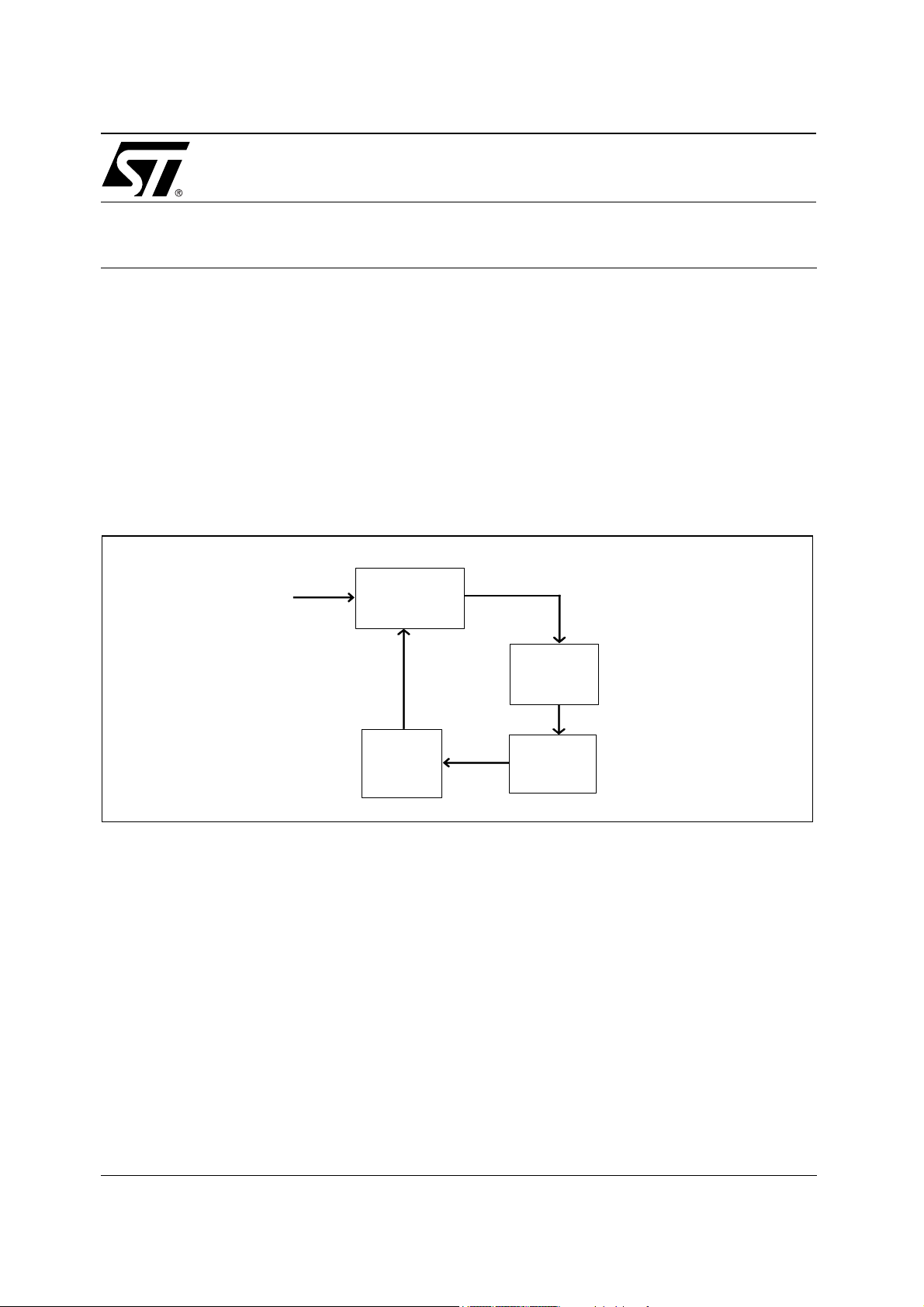
Figure 1: Block diagram of the application
BUCK SECTION
+12V
STN790A
1N5821
STS3DPFS30
STSA1805
PUSH-PULL SECTION
PWM SECTION
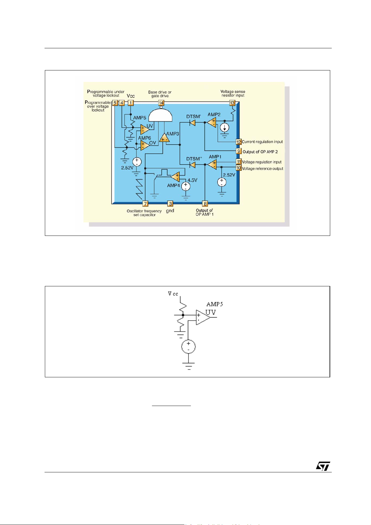
2. TSM108 DESCRIPTION
TSM108 is a PNP power bipolar or P channel power MOSFET controller. TSM108 includes a PWM
generator (AMP3 in fig. 2), voltage and current control loops (AMP1 and AMP2 respectively in fig. 2) and
it also includes safety functions that lock the PNP power bipolar or P channel power MOSFET in off
state. The TSM108 can sustain 60V on V
device) and I
(min value) and 30 mA (max value).
June 2004
(base or gate drive source current to switch off the device) are respectively 15 mA
source
TSM108
and the I
cc
(base or gate drive sink current to switch on the
sink
LAMPS
OUTPUT SECTI ON
Rev. 2
1/56
Page 2
AN1722 - APPLICATION NOTE
Figure 2: TSM108 schematic circuit
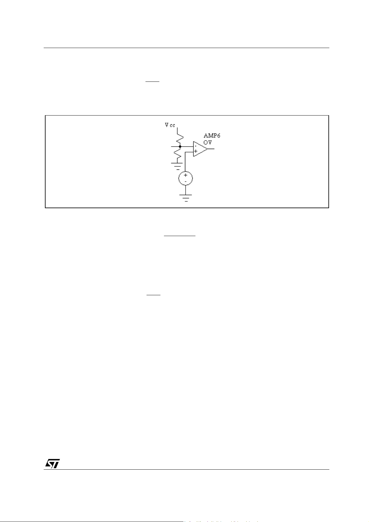
As exposed above, the safety functions UV and OV can switch off the power transistor (PNP power bipolar
or P channel power MOSFET) when the V
is under a definite min voltage or when the Vcc overcomes a
cc
definite max voltage. In fact, in these cases the output signal of the AMP 5, or the AMP 6, is low and the
NAND output is high. Considering the UV function, fig. 3 shows the circuit part concerning it.
Figure 3: UV schematic circuit detail
184kΩ
76.5kΩ
2.52V
The V
voltage (the one in the non-inverting pin of the AMP5) is:
+
5.76
V+=
+
V
cc
5.76184
(1.1)
and considering:
V
2/56
=2.52V (1.2)
-
Page 3
AN1722 - APPLICATION NOTE
the minimum V
under which the application will switch off is:
cc
V
52.2
cc
5.76
≈+=
(1.3)
V5.8)5.76184(
Considering the OV function, fig. 4 shows the circuit part concerning it.
Figure 4: OV schematic circuit detail
275kΩ
23.2kΩ
2.52V
The V
voltage (the voltage in the inverting pin of the AMP6) is:
-
2.23
V+=
−
V
cc
2.23275
(1.4)
and considering:
V
the maximum V
over which the board will switch off is:
cc
V
52.2
cc
2.23
= 2.52V (1.5)
+
(1.6)
≈+=
V4.32)2.23275(
In order to adjust the UV and OV voltages it is necessary to insert suitable resistances as showed later in
this paper.
It is important to highlight that, normally, the max δ (duty cycle) of the base drive, or gate drive, is around
95 %.
3. STN790A DESCRIPTION
The STMicroelectronics’ power bipolar transistor device STN790A is housed in the SOT-223 package.
Such device is manufactured in PNP planar technology using a 'Base Island' layout that involves a very
high gain performance and a very low saturation voltage.
The main characteristics of the STN790A device are:
1) V
2) V
3) V
4) I
5) I
≥ 30V
eco
≥ 40V
ecs
≥ 5V
beo
= -3 A (continuous current)
c
= 1 A (continuous current)
b
3/56
Page 4

AN1722 - APPLICATION NOTE
6) V
7) H
= 1.2 mV (typ) @ Ib = -20 mA @ Ic = -2 A (typical conditions)
ec(sat)
= 100 (min) @ Ic = -2.5 A @ Vec = 3V (typical conditions)
fe
4. 1N5821 DESCRIPTION
The STMicroelectronics’ SCHOTTKY diode is integrated in the package DO-201AD and has very small
conduction losses, negligible switching losses and extremely fast switching.
The main characteristics of the 1N5821 device are:
1) V
2) I
RRM
= 3A
F
≥ 30V
5. STS3DPFS30 DESCRIPTION
The STS3DPFS30 device is mounted inside a P channel power MOSFET, using the STripFET layout that
allows a lower Rds(on) and a SCHOTTKY diode. It is housed in the SO-8 package.
The main characteristics of the STS3DPFS30L device are:
1) V
≥ 30V
sd
≥ 20V
2) V
sg
3) R
ds(on)_max
= 3A (integrated diode);
4) I
F
5) V
F_max
6) V
RRM
= 0.09 Ohm @ Id = 1.5 A @ Vsg=10V
= 0.51 V (integrated diode)
= 30V (integrated diode)
6. STSA1805 DESCRIPTION
The STMicroelectronics’ power bipolar transistor device STSA1805 is housed in the TO-92 package.
Such device is manufactured in NPN planar technology using a 'Base Island' layout that involves a very
high gain performance and a very low saturation voltage.
The main characteristics of the STSA1805 device are:
1) V
2) V
3) V
4) I
5) I
6) V
7) H
≥ 60V
ceo
≥ 150V
ces
≥ 7V
ebo
= 5A (continuous current)
c
= 1A (continuuous current)
b
= 140 mV (typ) @ Ib = 50 mA @ Ic = 2A (typical conditions)
ce(sat)
= 270 (typ) @ Ic = 2A @ Vce = 1V (typical conditions)
fe
7. APPLICATION INTRODUCTION
The CCFL applications (Cold Cathode Fluorescent Lamp) are generally used for the monitor back lighting
which is often used to illuminate the signs.
The part of the circuit driving the CCFL lamps is composed of a DC-AC converter. The CCFL applications
use special compact fluorescent lamps. The lamps number can be 1, 2, 4, or 6 and the output power can
be in the range of 2-24W. The DC-AC converters transform the low DC in input voltage in necessary high
AC output voltage for the fluorescent tubes. The CCFL are usually powered with a 12 V
voltage.
dc
4/56
Page 5
AN1722 - APPLICATION NOTE
Today, two topologies are available for driving the above-mentioned special tubes: the 'ROYER' and the
FULL BRIDGE solutions.
The 'ROYER' solution uses a Push-Pull current fed converter where the current source is due to an
inductor and where it is possible to regulate the lamps brightness. Such a regulation is carried out by
means of the inductor current controls, through a PNP power bipolar or P channel power MOSFET
transistors (STN790A or STS3DPFS30 respectively), working in PWM mode, and a free wheeling diode.
The diode, the transistor and the inductor make a BUCK converter stage before of the PUSH-PULL
converter stage. The PUSH-PULL converter uses two NPN power bipolar transistors (STSA1805). The
other solution, the FULL BRIDGE topology, uses four power MOSFET transistors, two pair of
complementary power MOSFET transistors, driven by a suitable IC.
The design described in this paper uses the 'ROYER' topology, thus, only such topology will be studied.
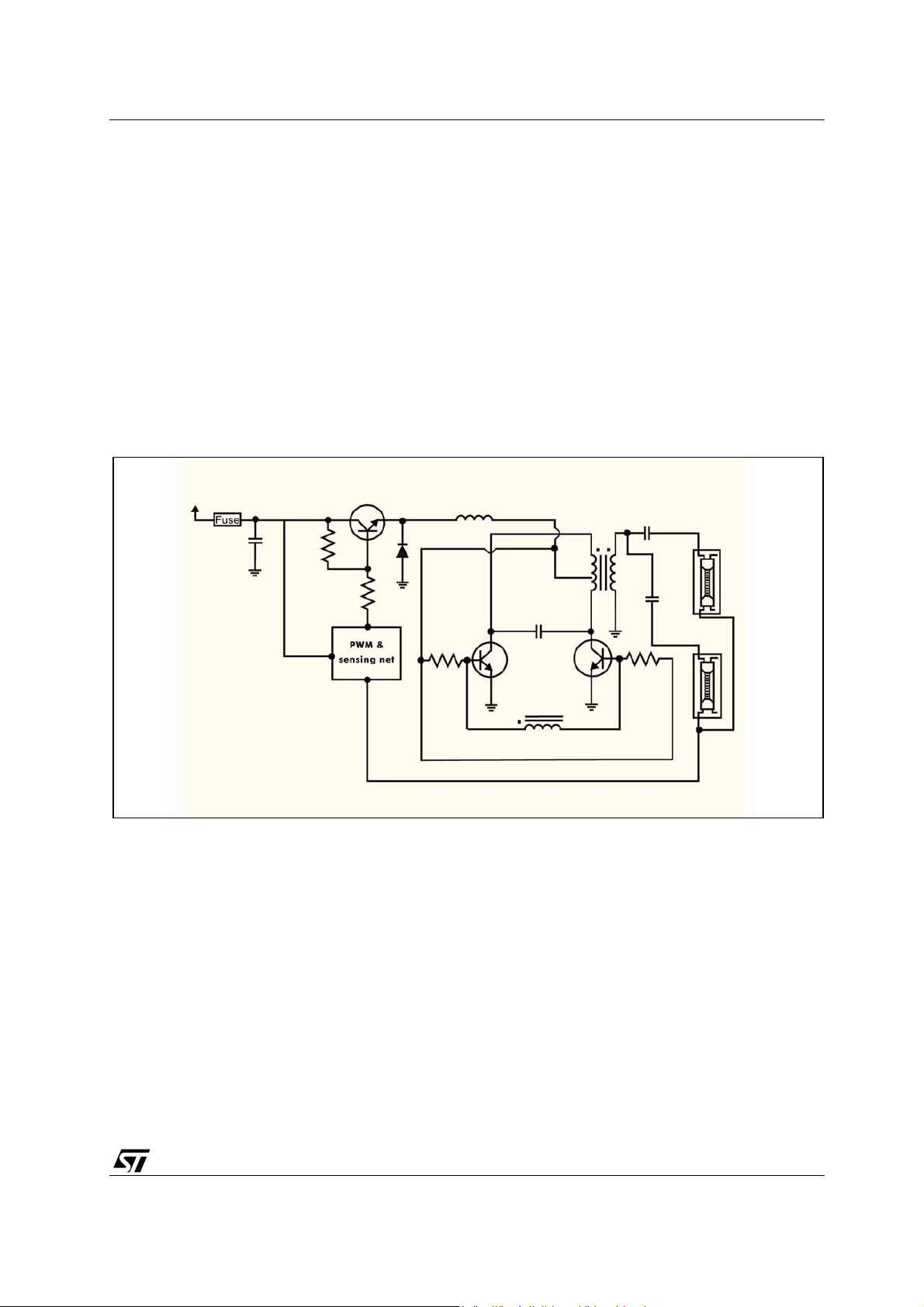
In the graph below a schematic circuit of a CCFL application, using two paralleled 6W lamps and only one
transformer, is shown (this is one of the several possible output stage configurations).
Figure 5: 'ROYER' converter schematic circuit
8. FLUORESCENT TUBES CHARACTERISTICS
Fluorescent lamps are generally made with tubes filled with a gas mixture at low pressure. The inner
sides of the tubes are covered with fluorescent elements. During the start-up, before the tube lights on,
the lamp has a very high resistance. Usually, in the common fluorescent lamps, the electrodes voltage
increases up to around 500V and starts to warm up and emit ions, but in the CCFL tubes the voltage
between the lamp electrodes reaches up to 1300V. Fig. 6 shows CCFL lamp characteristics before the
striking.
5/56
Page 6
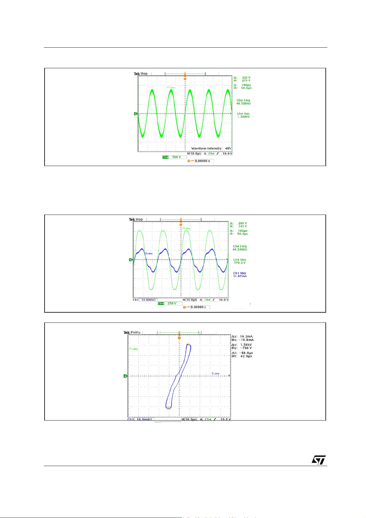
AN1722 - APPLICATION NOTE
Figure 6: Lamp voltage before striking
When the fluorescent lamp lights on, the gas mixture inside is fully ionized, and an arc across the two
electrodes occurs. In this new condition, the lamp resistance drops to 60 KOhm and the voltage across
the lamps drops to about 800V (Fig. 7 and Fig. 8 show the lamp characteristics and the V-I characteristic
respectively after the striking).
Figure 7: Voltage and current Lamp after striking
Figure 8: V-I Characteristic after striking
After the striking, the gas mixture emits radiations able to excite the fluorescent elements inside the tube
producing the light in the visible spectrum. In this example, after the striking, the maximum electrodes
voltage falls from 1300V down to 770V with a peak current of 12 mA. In the common fluorescent lamp
6/56
Page 7

AN1722 - APPLICATION NOTE
π
π
π
the voltage between the tube terminals drops from about 500V, before the striking, to about 220V after
the striking.
Usually, after the striking, in order to increase the light efficiency, the tube works with a frequency around
25-50KHz, in fact, in this frequency range, the light output can increase up to 15 % for the same input
energy.
Generally, the common fluorescent lamps can be considered only as a resistive load. In the CCFL lamps,
instead, even if the tubes show a resistive behavior, a small but evident capacitive behavior is observed
as it is shown in fig.7. In fig. 7 it is evident that the V-I Characteristic is linear until the established voltage
value is reached (in this case about 500V). After reaching this voltage value, the characteristic starts to
become flat because no ion can emit other radiations.
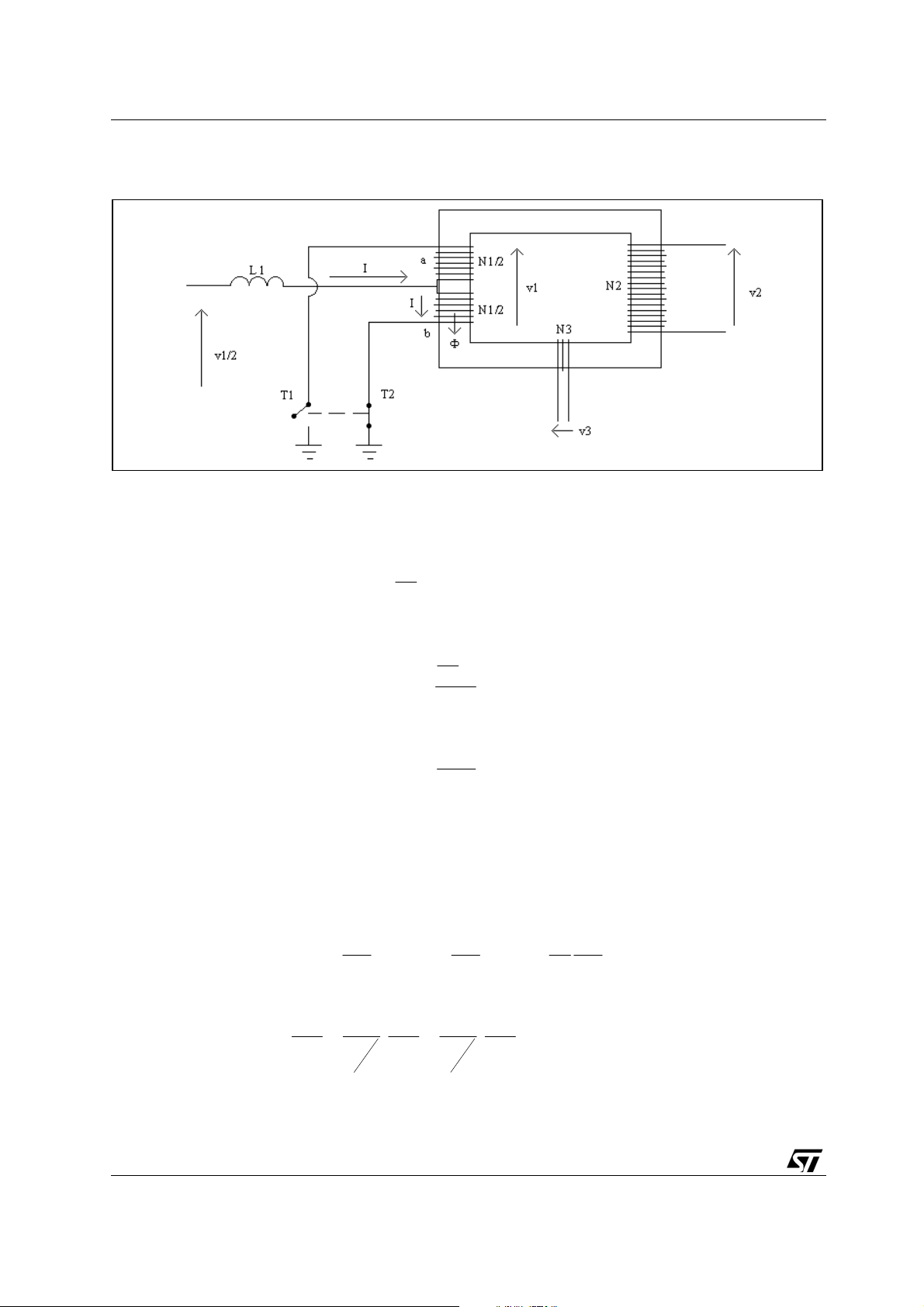
9. TRANSFORMER DESCRIPTION
The transformer named T
connected to the collectors of the Q
has a central terminal where the inductor L
shown in fig. 5 has three windings. The primary winding terminals are
1
and Q3 NPN power bipolar transistors. The same primary winding
2
output is connected. The secondary winding terminals are
1
connected to the loads.
The third winding terminals are connected to the base of the transistors Q
while the second is off and vice versa. During the Q
the related half primary winding, instead, when Q
on state the current flows through the device and
2
is on the current passes through this second device
3
and the other half primary winding. Usually the LT primary inductance of the transformer T
compared to the inductance L
LT inductance. In the design, N
ratio is around 80-90 while, N
12 V
input voltage, the v
dc
. The resonance frequency of the PUSH-PULL converter is also due to the
1
(number of secondary turns) and N1/2 (number of half primary turns)
2
/2 and N3 (number of third turns) ratio, is around 4-5. In fact, considering a
1
voltage (the max voltage between the terminal of the central point of the
1/2max
and Q3 so that the first is on
2
is much lower
1
primary winding and the reference when the PNP power bipolar or the P channel power MOSFET
transistors are always on) is:
as then demonstrated around 19V, the v
Vv ⋅=
max2/1
(the max voltage between the secondary terminals of the
2max
dc
2
(9.1)
transformer) is:
N
Vv
max2
⋅=
2
2
dc
N
1
(
2
(9.2)
)
around 1500-1700V and the v
(the max voltage between the terminals of the third transformer
3max
winding) is:
N
)(
Vv
max3
⋅=
2
3
dc
N
1
(9.3)
2
As exposed above, the N
/2 value and not N1 is highlighted. In order to understand the reason of it, it is
1
7/56
Page 8
AN1722 - APPLICATION NOTE
∆
∆
necessary to consider the graph below.
Figure 9: Detail of the transformer T
1
As already exposed, when the Q
where the T
and generates a magnetic force (Hopkinson law):
switch is on, the I current passes through the 'b' half primary winding of the transformer T
2
transistor is on, the other is off and vice versa. Now, considering fig. 9
2
N
1
Φ⋅ℜ=⋅I
(9.4)
2
where Φ is the magnetic flux and ℜ is the magnetic reluctance of the T
N
1
⋅=ΦI
2
(9.5)
core, thus Φ is:
1
ℜ
The magnetic reluctance ℜ is:
=ℜ
µ
where µ is the core permeability, A is the core section and l is the core length. When T
T
switches on, the current flows through the other half primary winding 'a' of the transformer T1 and the
1
flux Φ inverts its direction. Such a flux flows in the magnetic core T
windings N
voltages v
and N3, and also with the other half of the primary windings N1/2, and generating the
2
and v3 (magnetic law-Lenz law):
2
∆Φ
−=
Nv
∆
t
−=
Nv
(9.6)
Al⋅
switches off and
2
creating a link respectively with the
1
Φ
;;
v
∆
t
−=
2/13322
N
Φ
1
2
(9.7)
t
∆
1
thus:
v
v
v
v
8/56
N
N
2
,
v
1
2
2
2/1
N
3
N
1
2/1
1
3
v
2
2,
===
2/1
(9.8)
Page 9

AN1722 - APPLICATION NOTE
=
=
=
Furthermore, the current i2 (the current flowing through the secondary winding of T1) is:
N
1
(9.9)
2
Ii =
2
N
2
in fact, the apparent input power is:
IVA
in 2/1
(9.10)
while the apparent output power is:
(9.11)
iVA
out
22
and considering an ideal transformer:
IViV
(9.12)
2/122
and thus:
N
V
i 1
V
I
1
2/12
2
2
2
(9.13)
===
kN
10. THE 'ROYER' CONVERTER TOPOLOGY
As previously exposed, the topology solution for CCFL applications used in this paper is the 'ROYER'
topology. This topology solution has a current feed PUSH-PULL switching converter stage and also an
inductor that together with a PNP power bipolar, or P channel power MOSFET transistor and a free
wheeling diode, makes a BUCK converter stage before the PUSH-PULL stage. The PNP power bipolar,
or the P channel power MOSFET transistor fixes the output power and thus the lamps brightness. All this
is performed through a PWM signal able to drive either the PNP bipolar transistor or P channel MOSFET
depending on the kind of device used. In order to implement the PWM of the transistor it is necessary to
make an output current sensing (the lamps current) and to compare such a signal to the reference
voltage in the AMP1 (see fig. 10 and fig.11 for the schematic circuit designed in this paper using the PNP
power bipolar transistor STN790 and the power MOSFET transistor STS3DPFS30 respecticvely). The
reference is fixed to 2.52V by the TSM108 internal voltage generator.
9/56
Page 10
AN1722 - APPLICATION NOTE
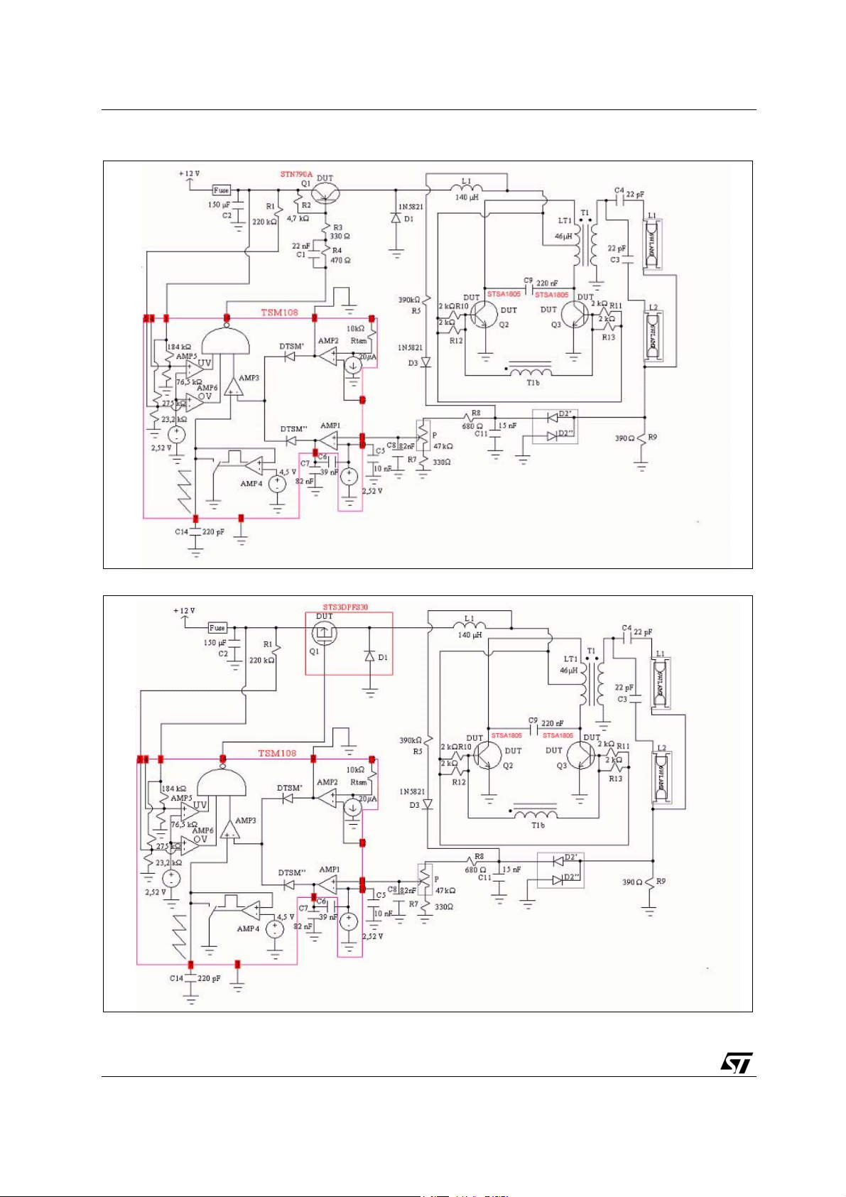
Figure 10: CCFL schematic circuit using the PNP power bipolar transistor
Figure 11: CCFL schematic circuit using the P channel power MOSFET transistor
Such a sensing net fixes also the right output power during the voltage net fluctuations.
10/56
Page 11
AN1722 - APPLICATION NOTE
=
The component values for capacitors, resistors, and inductors are selected based on the load power, the
operation frequency of the lamp before and after the striking (the operation lamp frequency must be in
the range of 25-50Khz), and the current ripple. The PNP power bipolar, or the P channel power MOSFET
operation frequency is fixed by means of the 220 pF capacitor C
Before the lamps strike the operation frequency is due to the resonance between the capacitor C
the primary transformer windings inductance LT of the T
transformer (see fig. 12):
1
(around 90KHz).
14
and
9
f
=
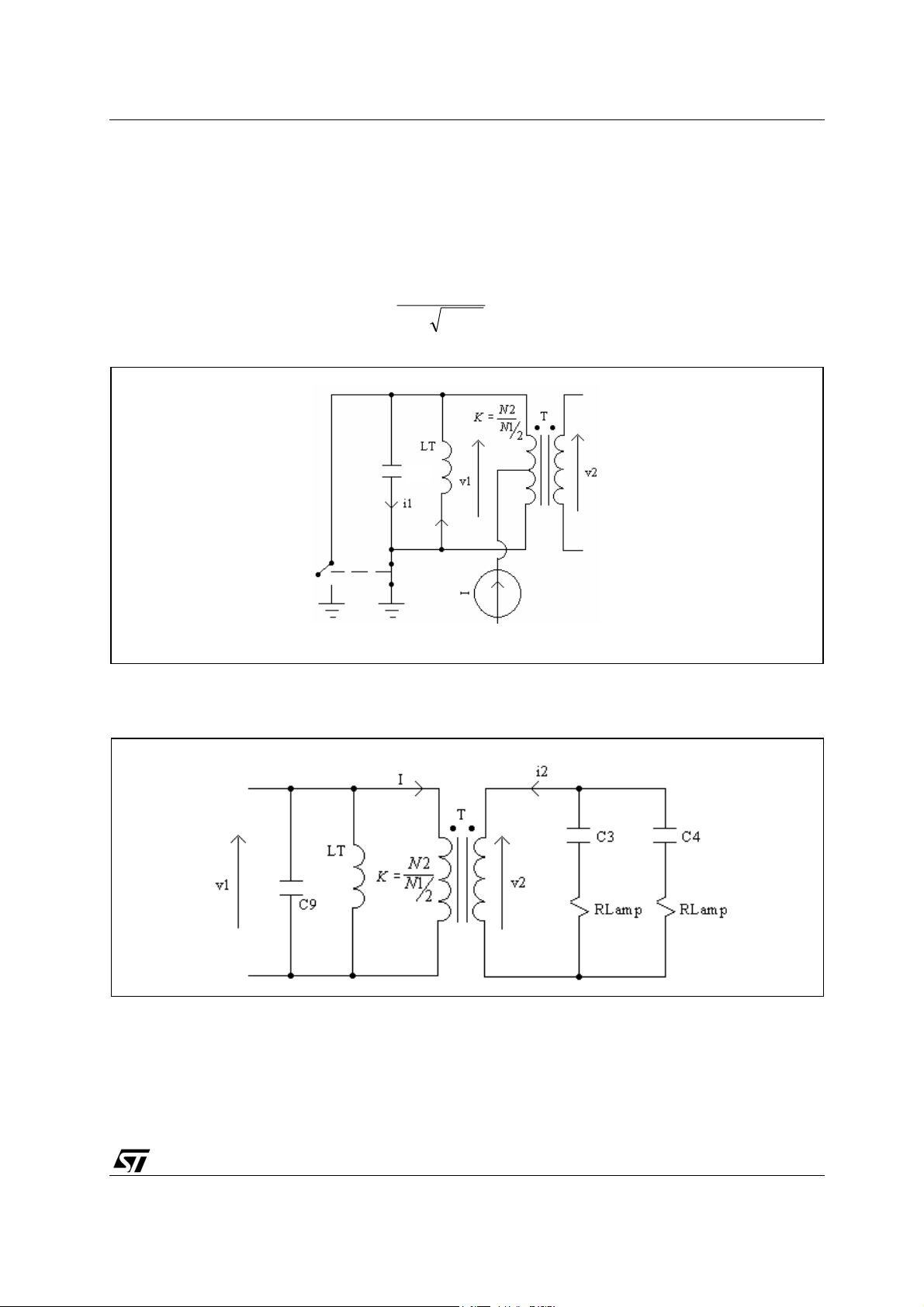
Figure 12: Resonant schematic circuit before lamps striking
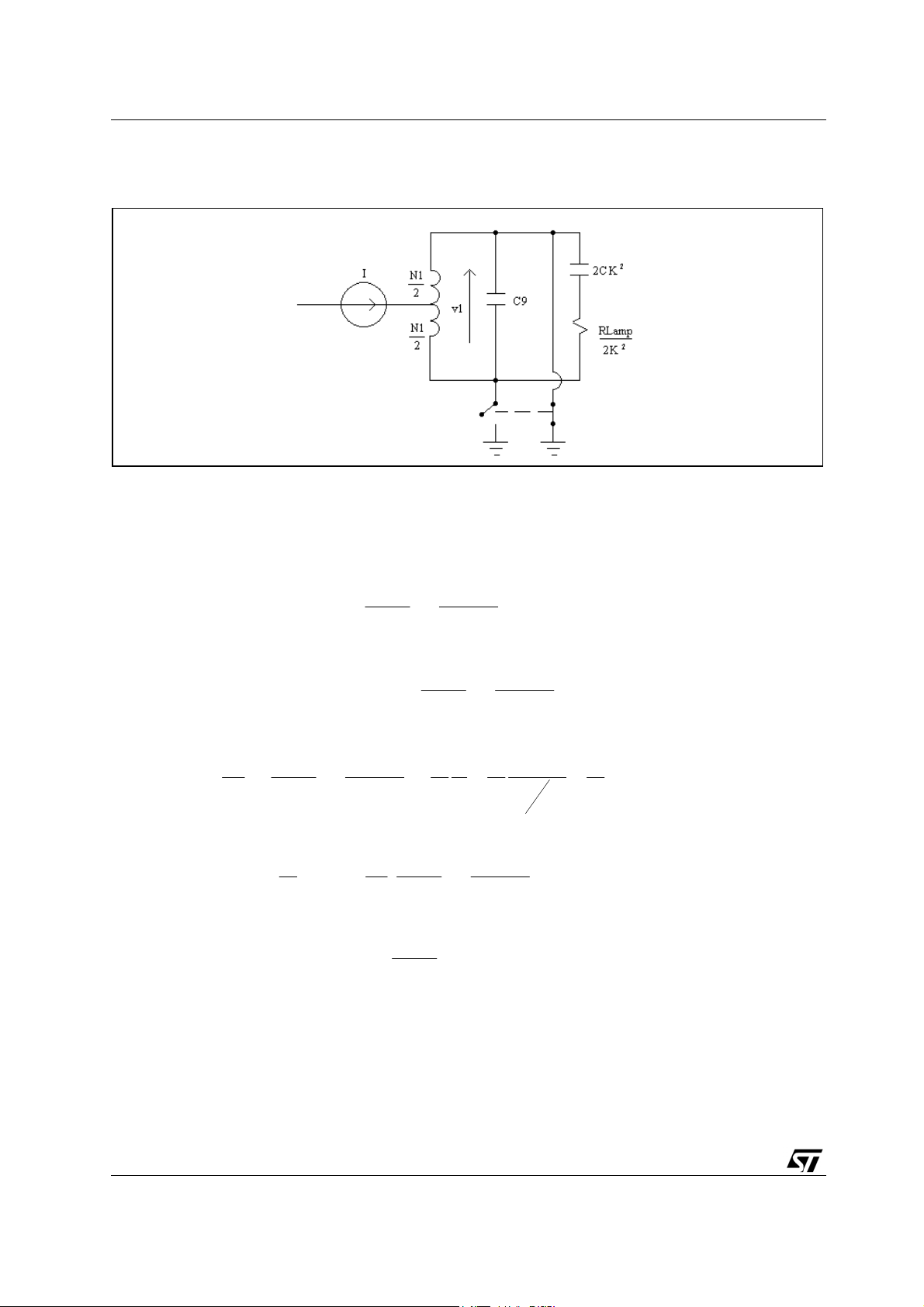
When the lamps are connected, the transformer circuit, considering the ideal transformer, can be
represented as in the following graph.
Figure 13: Resonant circuit of the transformer after lamps striking
1
2
LTC
π
⋅
C9
9
(10.1)
In this condition, the apparent input power is:
IvA
(10.2)
1in
11/56
Page 12
AN1722 - APPLICATION NOTE
Now it is possible to consider a new equivalent transformer circuit as shown in the graph below and
where the apparent power is the same as before.
Figure 14: Equivalent resonant circuit of the transformer after lamps striking
In this equivalent transformer circuit the output impedance is transferred from the secondary winding to
the primary winding of the transformer T
(C3=C4=C) and that R
the C
4-Rlamp
net are in parallel configuration, the output impedance can be written as:
is the same for both lamps, considering also that the C3-R
lamp
. In fact, considering that C3 and C4 have the same value
1
net and
lamp
R
Lamp
2
but:
thus:
R
and thus:
IV
1
2
i
2
Lamp
( k
−=
2
V
1
z
I
where:
is the primary equivalent resistance, while:
1
j
2
C
ω
⋅⋅
1
1
eq
(
2
k
2
iiVIV
2221
)
R
R
Lamp
2k
2Ck
−
R
(
Lamp
2
2
j
Lamp
2
V
2
1
C
⋅⋅
ω
2
−==
1
iIi
22
j
−==
2
(10.7)
(10.8)
j
V
ω
(10.3)
1
2
C
⋅⋅
ω
N
21
N
I
1
(
2
1
)
C
⋅⋅
(10.4)
)
2
V
2
1
===
2
I
)
(10.6)
(10.5)
is the primary equivalent capacitance.
12/56
Page 13

AN1722 - APPLICATION NOTE
∆
Now, the equivalent primary admittance (Yeq1) is:
2
2
j
−
=
LT
ω
⋅
2
where:
Y
eq
+
is the admittance of the series net:
R
Lamp
k
Considering the impedance of the
2
negligible compared to Ck
possible to find the frequency that maximizes the Y
frequency is the resonance frequency of the application during the lamps on state):
, deriving the Yeq1 with respect to the pulsation ω and equaling to zero, it is
2
jCR
2
ω
ω
−
⋅
Lamp
22Ck
Cj
+⋅+
91
+
Cjk
)1(
ω
2
R
Lamp
2
k
and, thus, minimizes the Z
eq1
ω
CRj
ω
(10.10)
(10.11)
Cjk
Lamp
(10.9)
)1(
impedance (such
eq1
2
ω
≅
and thus:
f+⋅≅
π
When the board is powered, the resistances R
Q
and Q3 and the lamps turn on. After the start-up, during the Q2 on state, the current flowing through
2
the inductance L
increases with an angular coefficient given by:
After a first instant, the current curve becomes flat and its average value depends on the impedance Z
and on the output power. However, when the PNP power bipolar, or P channel power MOSFET is on,
after the lamps start-up, the current oscillates around the average value because the ripple on it depends
only on the inductance L
transistor.
, through the half primary winding of the transformer T1 and through the transistor Q2,
1
=α
tg
. In PWM mode, instead, it depends also, linearly, on the duty cycle of the
1
1
)2(
2
CkCLT
(10.12)
(10.13)
)2(2
(10.14)
2
9
CkCLT +
1
9
and R11 (see fig. 15) enable the power bipolar devices
10
t*v
1L
L
1
eq1
13/56
Page 14
AN1722 - APPLICATION NOTE
Figure 15 shows the 'ROYER' converter schematic circuit during the start-up considering the current I
graph through the inductor.
Figure 15: 'ROYER' converter schematic circuit with inductor current theoretical
behavior at star- up
After the striking, the primary current ‘I’ generates the current i
transformer T
. At the beginning, the current i2 can be written as:
1
v
R
Lamp
2
(10.15)
i
=
2
into the secondary winding of the
2
2
because the capacitors C
the current i
drops to zero, while vc3 and vc4 reach the maximum voltage. At this time, the current i
2
inverts its direction and the capacitors C3 and C4 start discharging until the charge inside them becomes
zero and the current i
direction also the voltage v
current ‘I’ starts flowing into the other half winding of the transformer T
and C4 are discharged. Immediately after, these capacitors get charged and
3
reaches its maximum negative value. Furthermore, when the current i2 inverts the
2
reverts the polarities so that Q2 switches off, Q3 switches on, and the
t1b2
(see fig. 16).
1
2
14/56
Page 15
AN1722 - APPLICATION NOTE
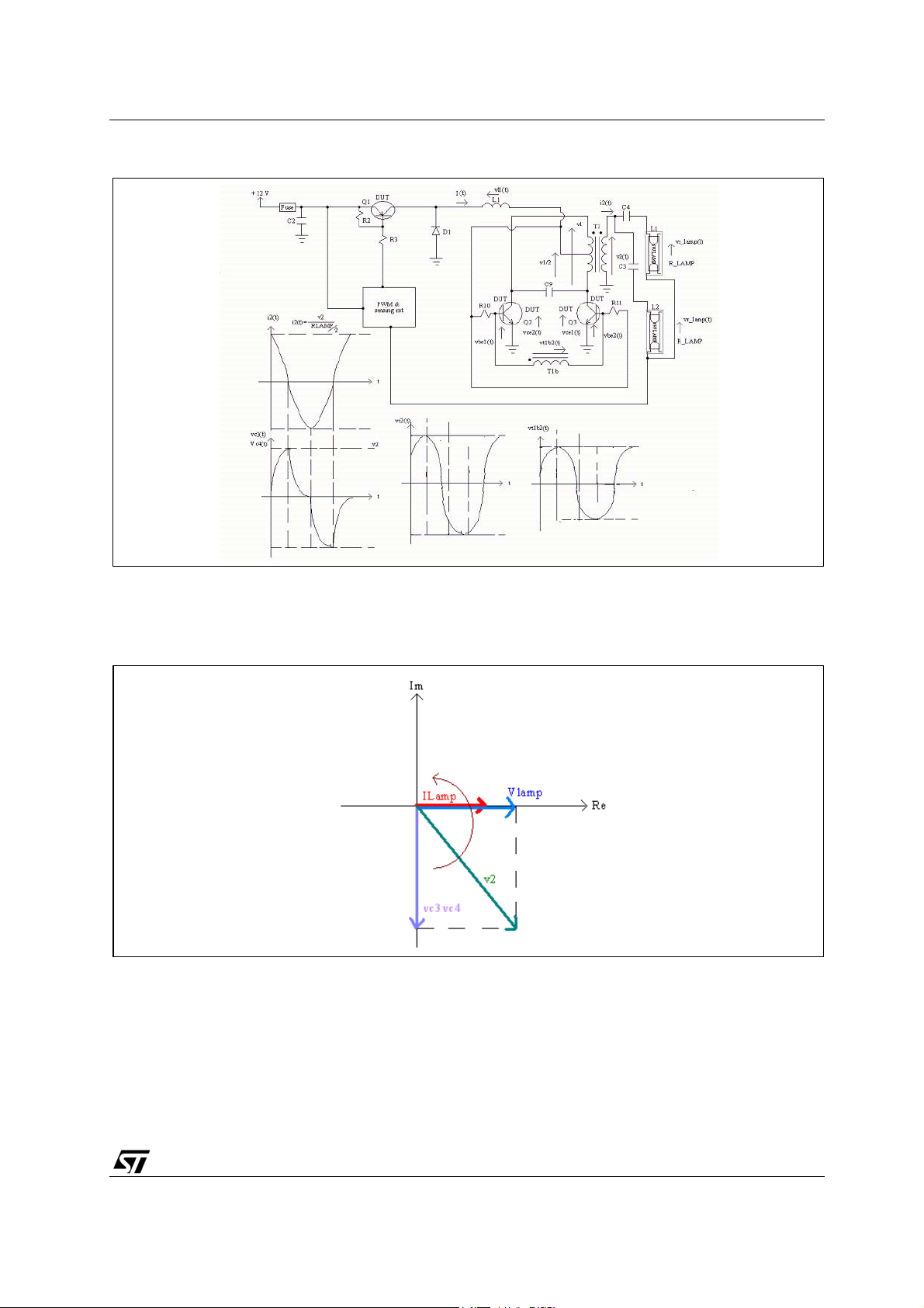
=
Figure 16: 'ROYER' converter schematic circuit with theoretical behavior of v1, v2, and i
The main output electrical parameters v2 (t), I
voltages across the capacitors C
and C4) are shown in the following graph under a vectorial
3
Lamp
(t), V
(t), vc3(t) and vc4(t) (these last two are the
Lamp
representation.
Figure 17: Vectorial representation of v
, i2, v
2
, vc3 and v
lamp
c4
2
In fact, assuming that, the lamps have only resistive behavior, the I
and the V
The graph also assumes that the vectors V
consideration. The I
(the voltage across them) can be written as:
lamp
Lamp
currents flow also through the capacitors C3 and C4 and, thus, the voltages v
Lamp
R*IV
LampLampLamp
and I
(10.16)
are on the real axis at the time taken into
Lamp
currents flowing through them
Lamp
c3
15/56
Page 16
AN1722 - APPLICATION NOTE
−
=
and vc4 can be represented as -90 º phase shifted vectors compared to the I
is the vectorial sum between the V
are very high compared to reactance of C3 and C4, the currents I
very much comparable to the voltage v
striking, R
one, thus making the voltages v
after the striking, the max V
The voltage v
drops to about 60 KOhm and the reactance C3-C4 becomes higher compared to the first
lamp
c3
must be about 700V across the tubes.
lamp
(voltage across the inductor L1) is the difference between the Vdc and the v
l1
and vc3, or vc4. Before the striking, the resistance lamps R
Lamp
are low and the voltages V
Lamp
across the secondary winding of the transformer T1. After the
2
and vc4 comparable to v2. However, in order to keep the lamps on,
vectors. The voltage v
Lamp
lamp
voltages
1/2
lamp
are
considering the PNP power bipolar in on-state, or the P channel power MOSFET transistor (see fig. 18).
, v
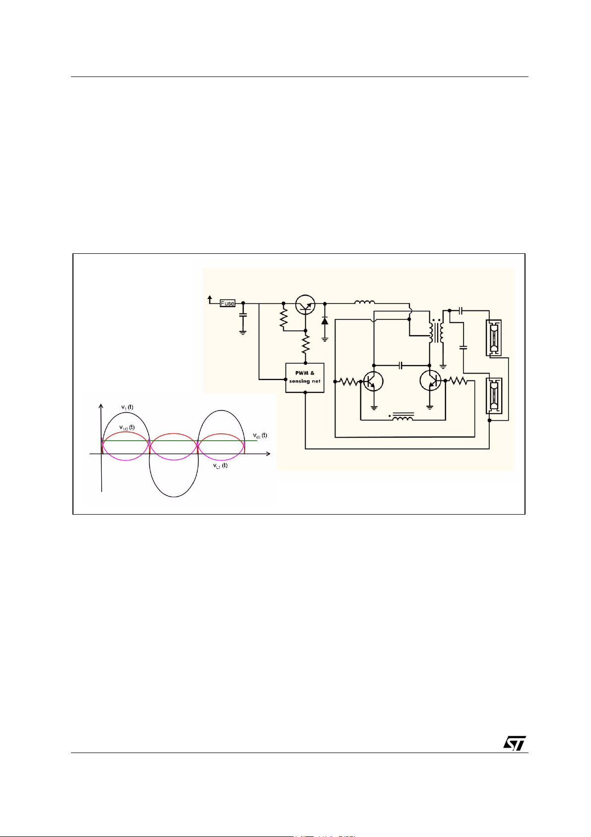
Figure 18: 'ROYER' converter schematic circuit with the theoretical behavior of v
V
dc
1
, vL1, and
1/2
2
During the off state of the transistor Q1, the diode D1 turns on and the voltage vL1 becomes:
vv
16/56
(10.17)
2/11L
Page 17
AN1722 - APPLICATION NOTE
Figure 19: v1, v
off and the diode D1 freewheels
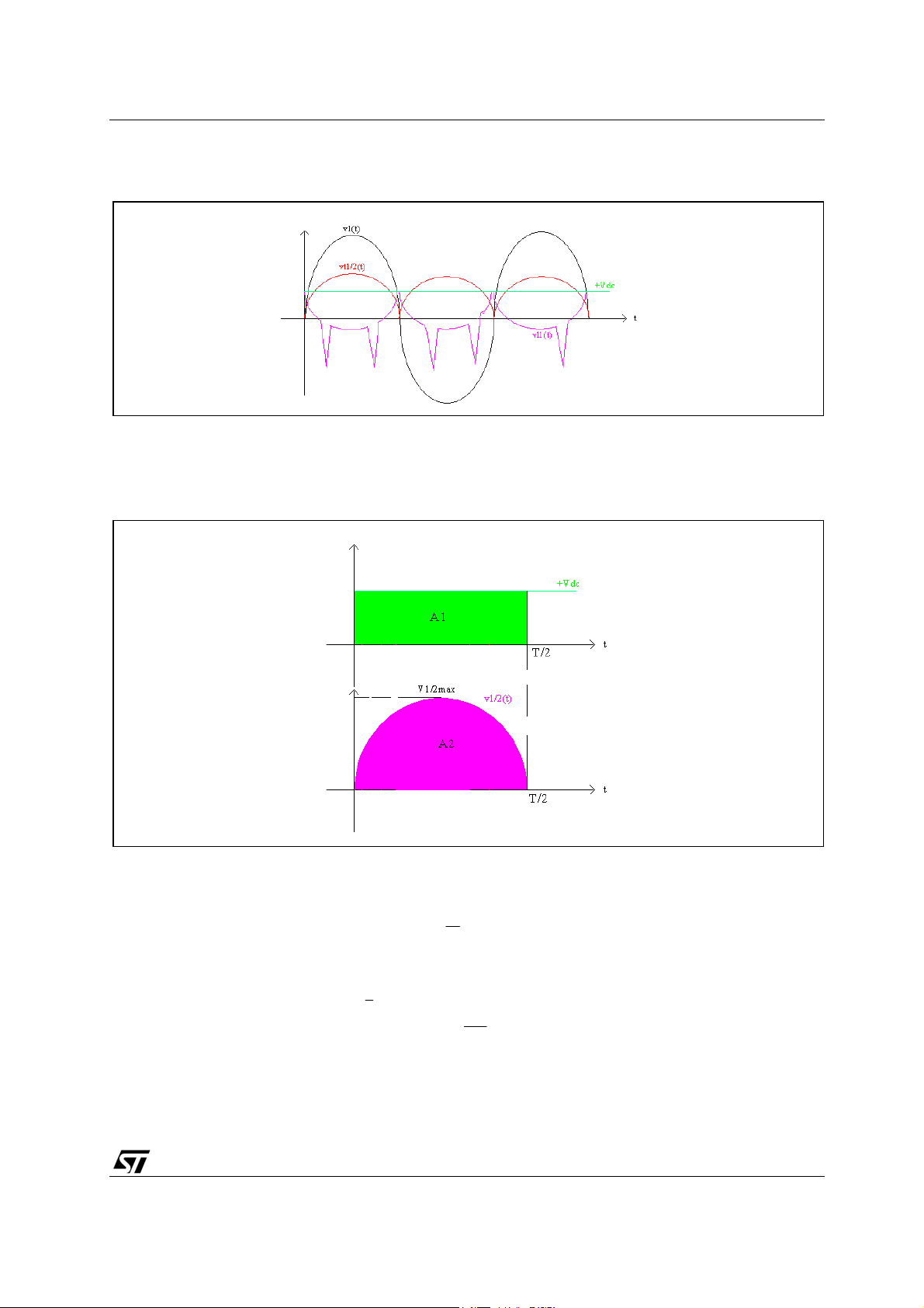
In fact, supposing Q1 always in on state, focusing the attention only on one half-period of the periodic
voltage v
voltage v
Figure 20: v
, as showed in fig. 20, the area A2 must be equal to the area A1 because the half-sine wave
1/2
and the voltage Vdc must have the same average value.
1/2
half-sine wave and Vdc graphs
1/2
, and Vdc theoretical behavior when the P channel power MOSFET switches
1/2,vL1
So writing A
and considering A
as:
1
T
=
2:
T
2
=
max2/12
∫
0
(10.18)
VA
dc1
2
2
(senVA
π
dt)t
(10.19)
=
T
17/56
Page 18

AN1722 - APPLICATION NOTE
π
⋅π=
π
⋅⋅=
π
δ
T
2
T
=
2
π
A
T
V
2
and finally, the max voltage v1 is:
During the half-period T/2, Q1 can switch off and, in this short time, any voltage is supplied to the board.
Fig.21 shows a possible example.
Figure 21: v
half-sine wave and Vdc graphs when δ ≠ 100%
1/2
−
max1
T
=
π
2
cos([V
π
T
VV
Vv
dcmax1
T
0
=
π
1=A2
=⇒
V
V
dcmax2/1max1dc
2
(10.22)
]t)
(10.19)
max2/1
(10.20)
(10.21)
In this condition, the voltages v
1/2max
and v
V
max1
where δ is the duty cycle of Q
Now focusing the attention only on one half-period of the voltage v
state (see fig. 22).
18/56
.
1
1max
become:
V
δ=
dcmax2/1
2
VV
d
c
(10.23)
(10.24)
and considering Q1 always in on
L1
Page 19

AN1722 - APPLICATION NOTE
∆=−
=
−−+
π
π
⋅
π
π
⋅
Figure 22: : vl1 theoretical behavior detail
As previously exposed, after the lamps striking, the current 'I' fluctuates around an average value, thus it
can be written:
(10.25)
−
where I
v
where v
The voltage v
where now T is the period of the voltage v
A + D = B + C (10.28)
and:
A = B (10.29)
because:
C = B, D = A (10.30)
The voltage v
is the average value current 'I' that involves:
avg
is the average voltage value across L1.
avg
is:
avg
v
=
avg
is:
L1
1
avgavg
minmax
= 0 (10.26)
avg
T
, and thus:
L1
senVVv
⋅−=
dcdcL
2
IIIII
CBDA
)(
2
(
)
t
(10.27)
(10.31)
T
and t' is the time when v
is zero:
L1
0 t
dcdc
2
2
(
senVV
⋅−=
)'
(10.32)
T
19/56
Page 20

AN1722 - APPLICATION NOTE
∆
∆=⋅
∆
∆
∆
π
⋅
π
⋅
Solving the equation t' becomes:
T
'
t
=
During the design of the application, the max current ripple of 'I' is fixed. Usually, the ∆I
40% of the average value of 'I', where:
I
and thus:
∆
Considering the Lenz law:
avg
it is possible to find L
(L1 minimum value) as:
min
L
During the time interval 0-t' the current 'I' increases of
arcsen
2
⋅
=∆
%max
avg
Lv
=
1
min
=
min1
I
∆
max
ππ
I
max
I
avg
III
max%max
I
max
t
∆
t
v
avg
I
max
)2(
(10.33)
(10.34)
(10.35)
(10.36)
(10.37)
2
is about 20-
max%
and the v
and thus:
Finally, L1
When PWM is used, the current ripple depends also on frequency and duty cycle of Q
lower compared to the case where Q
with regard to the ripple.
The attention will be now focused on the PNP power bipolar transistor, or P channel power MOSFET, on
and the diode D1. During the Q1 on-state, the diode D1 is disabled, 'I' flows through the same device,
Q
1
while during the Q
is:
avg
v
v
can be calculated as:
min
1
L
min
off-state 'I' freewheels into D1 (see fig. 23).
1
'
t
1
'
t
dtv
1
Lavg
0
1
t
'
2
=
I
∆
max
'
t
1
[
∫∫
'
t
0
T
'{
V
tV
is permanently in an on-state, therefore this is the worst condition
1
dcdcavg
4
T
'{
V
tV
dcdc
4
⋅−=⋅=
senVV
dcdc
2
2
cos(1[
−−⋅=
cos(1[
−−⋅
⋅
ππ
2
(
(10.38)
)]
dtt
T
)]}'
t
(10.39)
T
2
)]}'
t
(10.40)
T
. Such ripple is
1
20/56
Page 21

Figure 23: Q1 and D1 theoretical behavior
AN1722 - APPLICATION NOTE
With regard to Q
or Q3, when the first is on, the current flows through the device, while the second is off
2
and vice versa (see fig. 24).
Figure 24: Q
and Q3 voltages and currents theoretically calculated
2
21/56
Page 22

AN1722 - APPLICATION NOTE
11. SENSING NET AND PWM NET WITH TSM108
The following picture highlights the sensing net considering the CCFL design used in this paper.
Figure 25: Sensing circuitry detail
During the i
across R
positive half-sine-wave the current, mainly, passes through the resistance R9. The voltage
2
enables the diode D2' and the net C11-R8-P-R7-C8. When Q1 is in on-state the max output
9
power on the lamps reaches about 16W, thus, the i
i
eff
2
While its maximum value i
2max
is:
max2
The maximum voltage across R9, V
R
The maximum voltage V
is important because if it overcomes 9V it can make the TSM108 instable.
R9
R
P
R9
out
Lamp
is:
max29max9
≅=
16
60000
mAi 23216
(RMS current) is:
2eff
mA
16
≅==
3
−
91023390
≅⋅⋅=⋅=
ViRV
(11.1)
(11.2)
(11.3)
22/56
Page 23

Figure 26: VR9 theoretical behavior
AN1722 - APPLICATION NOTE
During the i
increasing the application efficiency. During the i
charged, keeps constant the voltage across it and discharges on the R
negative half-sine-wave, the diode D
2
carries the current bypassing the resistance R9 and
2''
positive half-sine-wave, the capacitor C11 gets
2
-P-R7 net during the i2 negative
8
half-wave.
The inverting input of the AMP1 is fixed at 2.52V and it tries to keep the non-inverting input at the same
voltage. When the output power increases, the current i
increases as well and the voltage in the
2
non-inverting input overcomes the 2.52V but, immediately after, the AMP1 output and TSM108 regulate
the duty cycle of Q
limiting the output power and in turn reducing the non-inverting input voltage to
1
2.52V.
Regulating the trimmer P, the lamps brightness can be regulated. In fact, increasing the trimmer P
resistance the lamps brightness can be decreased because the non-inverting input overcomes 2.52V
and TSM108 decreases the Q
duty cycle and vice versa. In the following figure the AMP1
1
characteristics are shown.
Figure 27: TSM108 AMP1measured waveforms
The capacitor C
keeps the voltage in the non-inverting input of the AMP1 constant, thus avoiding
8
23/56
Page 24

AN1722 - APPLICATION NOTE
situations of instability. The resistor R5 regulates the minimum output power on the lamps. It is
connected to the central point of the primary winding of T
diode D
P-R
value under the 40% of the nominal lamps power. C
while the C
whose cathode goes to the capacitor C11. The diode D3 avoids a current flowing from C11-R8-
3
net to the T1 transformer. Without this net, the minimum output power would never reach a
7-C8
7
is the voltage reference bias capacitor. The capacitor C6 allows the flickering of the lamps to
5
be avoided. The following picture shows the driving circuitry of Q
Figure 28: Q
driver circuitry
1
on one side, and, on the other side, to the
1
is the compensation capacitor of the AMP1 output,
.
1
The AMP1 output is the AMP3 inverting input and is compared to the saw tooth signal generated from
AMP4. The frequency of the saw tooth signal is established by the capacitor C
. In this design the
14
220pF capacitor generates a saw tooth signal with about 90KHz switching frequency. Usually the Q
switching frequency must be at least twice the lamps frequency. It can reach up to about 250 KHz using
a P channel power MOSFET. When the AMP1 output is higher compared to the saw tooth signal, the
AMP3 output is low and Q
switches on and vice versa. The following picture shows the AMP3
1
characteristics.
24/56
1
Page 25

AN1722 - APPLICATION NOTE
Figure 29: TSM108 AMP3 measured waveforms
It is important to highlight that such design allows the regulation of the output power on the lamps in the
2-16W range.
As considered in section 1, the TSM108 has the Q
lock functions UV (under voltage lockout) and OV
1
(over voltage lockout). Without any external components, as previously said, the input voltage range
accepted by the TSM108 is between 8.5V and 32.4V. In this application, being such voltage 12V, the
chosen voltage range is 8.5-15.5V. While the minimum input voltage value corrisponds to the standard
UV of the TSM108, being the maximum chosen input voltage lower than the standard OV, it is necessary
to introduce an external a 220KOhm resistor R1 between +12V and the pin 5 of the TSM108, in order to
decrease such value (see fig. 30).
Figure 30: OV modified circuit
25/56
Page 26

AN1722 - APPLICATION NOTE
Considering the equation 2.6, the OV voltage is:
52.2
2.23
52.2
)2.23220//275(
=+=
[(
2.23
220*275
220275
+
=+
VVcc 8.15]2.23)
(11.1)
12. DESIGN OF THE CCFL APPLICATION USING TSM108 AND THE STMicroelectronics' POWER
TRANSISTORS
In Table 1 all the components of the design, taken as an example, are listed. Figures 31 and 32 show the
schematic circuits of the application using the STN790A power bipolar and STS3DPFS30 respectively
and the TSM108.
Table 1: Components list
COMPONENT NAME VALUE
COMPONENT NAME VALUE
RESISTANCE R1
RESISTANCE R2 4, 7 kOhm
RESISTANCE R1
RESISTANCE R3 330 Ohm
RESISTANCE R2 4,7 kOhm
RESISTANCE R4
RESISTANCE R3 330 Ohm
RESISTANCE R5
RESISTANCE R4
RESISTANCE R7 330 Ohm
RESISTANCE R5
RESISTANCE R8 680 Ohm
RESISTANCE R7 330 Ohm
RESISTANCE R9 390 Ohm
RESISTANCE R8 680 Ohm
RESISTANCE R10 2 kOhm
RESISTANCE R9 390 Ohm
RESISTANCE R11 2 kOhm
RESISTANCE R10 2 kOhm
RESISTANCE R12 2 kOhm
RESISTANCE R11 2 kOhm
RESISTANCE R13 2 kOhm
RESISTANCE R12 2 kOhm
CAPACITOR C1 22 nF
RESISTANCE R13 2 kOhm
CAPACITOR C2 150 uF
CAPACITOR C1 22 nF
CAPACITOR C2 150 uF
CAPACITOR C3 22 pF
CAPACITOR C3 22 pF
CAPACITOR C4 22 pF
CAPACITOR C4 22 pF
CAPACITOR C5 10 nF
CAPACITOR C5 10 nF
CAPACITOR C6 39 nF
CAPACITOR C6 39 nF
CAPACITOR C7 82 nF
CAPACITOR C7 82 nF
CAPACITOR C8 82 nF
CAPACITOR C8 82 nF
CAPACITOR C9 220 nF
CAPACITOR C9 220 nF
CAPACITOR C11 15 nF
CAPACITOR C11 15 nF
CAPACITOR C13 10 nF
CAPACITOR C13 10 nF
CAPACITOR C14 220 pF
STS3DFPS30-POWER MOSFET Q1
STS3DFPS30-POWER MOSFET Q1
STN790A-PNP P OW ER BIPOLAR Q1
STN790A-PNP P OW ER BIPOLAR Q1
STSA1805-NP N POW ER BIPOLAR Q2
STSA851-NPN POW ER BIPOLAR Q2
STSA1805-NP N POW ER BIPOLAR Q3
STSA851-NPN POW ER BIPOLAR Q3
CAPACITOR C14 220 pF
TSM108-IC
TSM108-IC
1N5821-DIODE D1
1N5821-DIODE D1
1N5821-DIODE D3
1N5821-DIODE D3
6 W LAMP l1
6 W LAMP l1
6 W LAMP l2
6 W LAMP l2
INDUCTOR L1 140 uH
INDUCTOR L1 140 uH
TRIMMER P 47 kOhM
TRIMMER P 47 k OhM
FUSE 2 A
FUSE 2 A
220 kOhm
220 kOhm
470 kOhm
390 kOhm
470 kOhm
390 kOhm
26/56
Page 27

AN1722 - APPLICATION NOTE
Figure 31: CCFL schematic circuit using the PNP power bipolar transistor
Figure 32: CCFL schematic circuit using the P channel power MOSFET transistor
27/56
Page 28

AN1722 - APPLICATION NOTE
The following graphs show the voltage characteristics of the transformer while no lamps are connected
to the converter.
Figure 33: v
measured waveforms before striking
2
Figure 34: v
measured waveforms before striking
1
28/56
Page 29

Figure 35: V3 measured waveforms before striking
≅⋅=
π
AN1722 - APPLICATION NOTE
Figure 36: v
In figure 34 the maximum value of v1 is 37V according to the formulas 10.22:
measured waveforms before striking
1/2
VVv
⋅=
ma
1
x
The operation frequency is about 50KHz, in fact, considering the formula 10.1:
f 50
=
1
LTC
π
⋅
2
9
dc
=
1
5,371214,3
⋅⋅⋅⋅
10220104614.32
(12.1)
Khz
≅
96
−−
(12.2)
29/56
Page 30

AN1722 - APPLICATION NOTE
π
The maximum voltage value of v
is 18.80V, as stated in formula 9.19:
1/2
14.3
dc
2
v
max2
v
2
The
N
N
1700
max2/1
80.18
The voltage v
characteristics.
max2/1
has a frequency twice the v1 because v
1/2
N
2
N
1
2
N
N
1
In fig. 37 the waveforms of current and voltage of L
Figure 37: v
, iL1 and iak measured waveforms before striking
L1
v
3
2
max3
v
max2/1
5.5
80.18
≅⋅=⋅=
N
3
2
,
N
1
1
2
2
90
≅==
1
≅==
3
are showed.
1
VVv
8.1812
1/2
ratio are:
(12.3)
has only half positive sin-wave
(12.4)
(12.5)
In this condition, the current I
while the maximum v
voltage is equal to Vdc. According to the formula 9.29 the minimum vL1 value is:
L1
into the inductor L1 is 1A. The vL1 frequency is the same as the v
L1
Vv
−=
As showed in fig. 37, the minimum v
off, the diode D
30/56
switches on (in fig. 37 the iak current is highlighted), and the voltage vL1 is -v
1
π
2
L1
12V
dcdcmin1L
value is about -18.5V because during the operation Q1 switches
14.3
V712
−≅−=
(12.6)
2
1/2
1/2
.
one,
Page 31

The following graph shows current and voltage in D1 in these conditions.
Figure 38: i
and vak measurements before striking
ak
AN1722 - APPLICATION NOTE
The pictures in the next pages show all voltages and currents when the lamps are connected.
Figure 39: v
measurement during the lamps on-state
2
31/56
Page 32

AN1722 - APPLICATION NOTE
Figure 40: v1 measurement during the lamps on-state
Figure 41: V3 measurement during the lamps on-state
32/56
Page 33

AN1722 - APPLICATION NOTE
Figure 42: v
The operation frequency drops from about 50KHz to about 35 KHz, in fact, considering the 10.13:
measurement during the lamps on state
1/2
f
=
1
2
9
=
⋅⋅+π⋅
)Ck2C(LT2
(12.7)
=
The obtained result theoretically is very much similar to the measured one and the slight difference is
mainly due to the simplifications applied in the mathematical model.
Fig.43 shows the current and voltage behavior when lamps are connected.
Figure 43: v
, iL1 and iak measurements during the lamps on-state
L1
1
12296
−−−
⋅⋅⋅+⋅⋅⋅
)109044210220(104614.32
Khz32
≅
33/56
Page 34

AN1722 - APPLICATION NOTE
Now, focusing the attention on Q1, considering the lamps on, the following figures show the power bipolar
STN790A and the power MOSFET STS3DPFS30 characteristics (steady state, turn off) considering three
different input voltages 12V (standard condition), 10.8V and 13.2V (+-10% of the nominal voltage
condition). The tables, following the graphs below, summarize the main electrical parameters.
Furthermore, waveforms regarding the free wheeling diode D
working under the same above-mentioned
1
conditions are included.
Figure 44: STN790A steady state (V
dc
=12V)
Figure 45: STN790A turn off (V
=12 V)
dc
34/56
Page 35

Figure 46: STN790A turn on (Vdc=12V)
AN1722 - APPLICATION NOTE
Figure 47: STS3DPFS30 steady state (V
=12V).
dc
35/56
Page 36

AN1722 - APPLICATION NOTE
Figure 48: STS3DPFS30 turn off (Vdc=12 V)
Figure 49: STS3DPFS30 turn on (Vdc=12V).
36/56
Page 37

Figure 50: STN790A steady state (Vdc=10.8V).
Figure 51: STN790A turn off (Vdc=10.8 V).
AN1722 - APPLICATION NOTE
37/56
Page 38

AN1722 - APPLICATION NOTE
Figure 52: STN790A turn on (Vdc=10, 8 V).
Figure 53: STS3DPFS30 steady state (V
=10,8 V).
dc
38/56
Page 39

Figure 54: STS3DPFS30 turn off (Vdc=10.8 V).
AN1722 - APPLICATION NOTE
Figure 55: STS3DPFS30 turn on (V
=10.8 V).
dc
39/56
Page 40

AN1722 - APPLICATION NOTE
Figure 56: STN790A steady state (Vdc=13.2V)
Figure 57: STN790A turn off (V
=13.2V)
dc
40/56
Page 41

Figure 58: STN790A turn on (Vdc=13.2V)
AN1722 - APPLICATION NOTE
Figure 59: STS3DPFS30 steady state (V
=13.2V)
dc
41/56
Page 42

AN1722 - APPLICATION NOTE
Figure 60: STS3DPFS30 turn off (Vdc=13.2V)
Figure 61: STS3DPFS30 turn on (V
=13.2V)
dc
42/56
Page 43

Figure 62: 1N5821 steady state (Vdc=12V)
AN1722 - APPLICATION NOTE
Figure 63: 1N5821 turn off (V
=12V)
dc
43/56
Page 44

AN1722 - APPLICATION NOTE
Figure 64: 1N5821 turn on (V
dc
igure 65: 1N5821 steady state (V
-12V)
=10.8V)
dc
44/56
Page 45

AN1722 - APPLICATION NOTE
Figure 66: 1N5821 turn off (V
Figure 67: 1N5821 turn on (V
=10.8V)
dc
=10.8V)
dc
45/56
Page 46

AN1722 - APPLICATION NOTE
Figure 68: 1N5821 steady state (V
Figure 69: 1N5821 turn off (V
=13.2V)
dc
=13.2V)
dc
46/56
Page 47

AN1722 - APPLICATION NOTE
Figure 70: 1N5821 turn on (V
-13.2V)
dc
47/56
Page 48

AN1722 - APPLICATION NOTE
Vce_sat@Ic=1 A an d Ib=15mA
Rds(on)@Id=1,15 A and Vsg=9 V
Hfe @ Ic=1 A and Vec=1 V
Turn-off Energy 974 nJ 649 nJ
Turn-on Energy 1508 nJ 375 nJ
Vce_sat@Ic=1 A an d Ib=15mA
Rds(on)@Id=1,15 A and Vsg=9 V
Hfe @ Ic=1 A and Vec=1 V
Turn-off Energy 905 nJ 652 nJ
Turn-on Energy 1634 nJ 387 nJ
Tab II: Main measured electrical parameters.
STN790A STS3DPFS30
Vdc 12 V typ 12 V typ
Idc 1 A 1 A
145 mV -----
----- 102 mOhm
169 -----
Frequency 90,0 Khz 89,7 Khz
Tcase 71 °C 49 °C
Turn-off time 204 ns 160 ns
Turn-on time 316 ns 375 ns
Ic_max 1,44 A -----
Id_max ----- 1,37 A
Duty cycle 79% 81%
Ibon
12 mA -----
Vsg ----- 11,5 V
Iboff_max
-16 mA -----
Vsd_max ----- 13 V
Vec_max 15 V -----
Tab III: Main measured electrical parameter s.
STN790A STS3DPFS30
Vdc 10,8 V 10,8 V
Idc 1,12 A 1,12 A
145 mV -----
----- 102 mOhm
169 -----
Frequency 89,8 Khz 90,0 Khz
Tcase 72 °C 47 °C
Turn-off time 204 ns 180 ns
Turn-on time 384 ns 104 ns
Ic_max 1,45 A -----
Id_max ----- 1,31 A
Duty cycle 90% 90%
Ibon
12,5 mA -----
Vsg ----- 10,3 V
Iboff_max
-16 mA -----
48/56
Page 49

AN1722 - APPLICATION NOTE
Tab IV: Main electrical parameters measured.
Vdc 13,2 V 13,2 V
Idc 0,89 A 0,89 A
Vce_sat@Ic= 1 A and Ib=15m A
Rds(on)@Id=1,15 A and Vsg=9 V
Hfe @ Ic=1 A and Vec =1 V
Frequency 89,8 Khz 89,7 Khz
Tcase 68 °C 50 °C
Turn-off Energy 1082 nJ 640 nJ
Turn-on Energy 1381 nJ 377 nJ
Turn-off time 204 ns 144 ns
Turn-on time 292 ns 100 ns
Ic_max 1,50 A ----Id_max ----- 1,34 A
Duty cycle 73% 74%
Ibon 15 mA -----
Vsg ----- 12,4 V
Iboff_max -16 mA -----
Vsd_max ----- 14 V
Vec_max 16 V -----
STN790A STS3DPFS30
145 mV -----
----- 102 mOhm
169 -----
The aim of the table below is to show how stable is the power delivered to the lamps. In fact, the maximum
power variation is always below 2% for fluctuations of input voltage of +/-10%.
Table V: Input power variation vs input voltage variation
Vdc Idc Pin Delta_power
12 V 1 A 12 W -----
10,8 V 1,12 A 12,1 W 0.83%
13,2 V 0,89 A 11,8 W -1.69%
Furthermore, considering the above graphs and tables it is possible to see that the operation frequency is
about 90 KHz, the duty cycle is in the range of 73-81% for all considered input voltages conditions, the
max Ic (Id) current is about 1.5A, the max V
Considering the STN790A device, the I
mA and the I
(bipolar transistor base current during turn-off) is about -16 mA. Such values are achieved
boff
bon
by means of a suitable STN790A polarization net, consisting in the R
avoids having I
outside the maximum rating established for TSM108 and, in the meantime, it minimizes
sink
(Vsd) voltage is about 14V.
ec
(bipolar transistor base current during conductions) is about 13
2-R3-R4-C1
components. Such net
the turn off losses of the transistor. In open air, the measured case temperature of STN790A and
STS3DPFS30 is about 70 °C and 50 °C respectively. Such difference in temperature between STN790A
and STS3DPFS30 is, in particular, due to the higher switching loss of the PNP power bipolar compared to
the P channel power MOSFET and, however, it can be considered acceptable.
On the other hand, it is important to highlight that, during the turn on and the turn off, using the P channel
power MOSFET, much more noise is observed compared to the PNP power bipolar switching behavior.
In the next graphs all the waveforms regarding STSA1805, mounted in PUSH-PULL converter, are
showed considering the three input voltages under analysis.
49/56
Page 50

AN1722 - APPLICATION NOTE
Figure 71: STSA1805 steady state (Vdc=12V)
Figure 72: STSA1805 turn off (V
=12V)
dc
50/56
Page 51

Figure 73: STSA1805 turn on (Vdc=12V)
AN1722 - APPLICATION NOTE
Figure 74: STSA1805 steady state (V
=10.8V)
dc
51/56
Page 52

AN1722 - APPLICATION NOTE
Figure 75: STSA1805 turn off (Vdc=10.8V)
Figure 76: STSA1805 turn on (V
=10.8V)
dc
52/56
Page 53

Figure 77: STSA1805 steady state (Vdc=13.2V)
AN1722 - APPLICATION NOTE
Figure 78: STSA1805 turn off (V
=13.2V)
dc
53/56
Page 54

AN1722 - APPLICATION NOTE
Figure 79: STSA1805 turn on (Vdc=13.2V)
Tab VI: Main electrical parameters measured.
Vdc 12 V typ
Idc 1 A
Vce_sat@Ic=1 A and Ib=35mA
Hfe @ Ic=1,4 A and Vec=1 V
Frequency 40,0 Khz
Tcase 41 °C
Turn-off Energy 1131 nJ
Turn-on Energy Negligible
Ic_max 1,58 A
Ibon
Iboff_max
Vce_max 31 V
STSA851 STSA851 STSA851
78 mV
305
35 mA
-122 mA
10,8 V
1,12 A
78 mV
305
40,3 Khz
41 °C
959 nJ
Negligible
1,45 A
35 mA
-121 mA
30 V
13,2 V
0,89 A
78 mV
305
40,4 Khz
41 °C
976 nJ
Negligible
1,39 A
35 mA
-126 mA
31 V
In the above graphs and table it is possible to see that the operation frequency is about 40KHz, the I
is about 35mA, the max Vce is about 32V and the max Ic is about 1.5A for all the powering conditions.
From the thermal measurement, the case temperature for STSA1805 is 41 °C.
bon
The measured case temperature of the TSM108 is 29 °C in all conditions, the ambient temperature is
25°C .
54/56
Page 55

AN1722 - APPLICATION NOTE
13. CONCLUSIONS
This paper has showed an example on how a CCFL application can be designed and realized using the
TSM108, the power bipolar transistors STN790A (or the Power MOSFET STS3DPFS30), STSA1805
and the SCHOTTKY diode 1N5821.
In particular, a detailed theoretical model of the system has been built and the validation of the results
has given confirmation of the decided approach. Based on the very good results achieved, this technical
paper offers a valid support to whoever is interested in designing such kind of lighting systems.
The application shows a very good operation and it is stable considering the several input voltage
conditions. The application uses the 'ROYER' topology and by means of a sensing circuitry it fixes the
lamps brightness considering a net fluctuation. In fact, for variations of +/-10% of the nominal powering
voltage, the application power variation is always less than 2%. Furthermore, acting on a P trimmer it is
possible to regulate the lamps brightness changing the PNP power bipolar duty cycle, or the P channel
power MOSFET one.
Such a design considers an output solution with two 6W lamps connected in parallel, but tuning the
capacitors and the resistors components any output topology, considering several lamps, can be
achieved using the same STMicroelectronics’ devices. This design allows, acting on the P trimmer, the
output power on the lamps to be fixed between the 2-16W range and the application is enabled when the
input voltage is in the range of 8.5-15.5V. The operation frequency of the transistor Q
, in the BUCK
1
converter part, is fixed at about 90KHz. The application shows a good electrical and thermal behavior
considering both the solutions with STN790A (PNP power bipolar) and STS3DPFS30 (P channel power
MOSFET). In particular, the measured case temperature of the device STN790A under open air
condition, is in the worst case about 70 °C compared to the 50 °C of STS3DPFS30 (such a device has
also an integrated SCHOTTKY diode included in the same package). The reason for the difference in the
case temperature measured on the two devices is due, in particular, to the higher switching losses of the
power bipolar transistor compared to the power MOSFET transistor, and anyway is acceptable for this
design. On the other hand, it is important to highlight that, during the turn on and the turn off, of the P
channel power MOSFET much more noise was observed compared to the PNP power bipolar. The
reason for such a behavior is mainly due to the higher speed of the MOSFET compared to the bipolar
transistor. The analysis results achieved in this experiment demonstrate that the TSM108 and the power
transistors STN790A, or STS3DPFS30, and the STSA1805 can be used in order to realize the CCFL
applications.
Table 6: Revision History
Date Revision Description of Changes
28-Apr-2004 1 First Release
18-Jun-2004 2 Some spelling mistakes were
corrected
55/56
Page 56

AN1722 - APPLICATION NOTE
Information furnished is believed to be accurate and reliable. However, STMicroelectronics assumes no responsibility for the consequences
of use of such information nor for any infringement of patents or other rights of third parties which may result from its use. No license is granted
by implication or otherwise under any patent or patent rights of STMicroelectronics. Specifications mentioned in this publication are subject
to change without notice. This publication supersedes and replaces all information previously supplied. STMicroelectronics products are not
authorized for use as critical components in life support devices or systems without express written approval of STMicroelectronics.
The ST logo is a registered trademark of STMicroelectronics.
All other names are the property of their respective owners
© 2004 STMicroelectronics - All rights reserved
Australia - Belgium - Brazil - Canada - China - Czech Republic - Finland - France - Germany - Hong Kong - India - Israel - Italy - Japan -
Malaysia - Malta - Morocco - Singapore - Spain - Sweden - Switzerland - United Kingdom - United States
STMicroelectronics GROUP OF COMPANIES
www.st.com
56/56
 Loading...