

Page 1
AN1714
Application note
ST7538Q FSK powerline
transceiver demonstration kit description
Introduction
The advantages in the implementation of a communication network using the same
electrical network that supplies all the elements of the network are evident. In the presence
of new wideband LANs using an RF system, for example Bluetooth, a narrowband
communication system using the mains has considerable advantages also.
It is widely accepted that in residential or industrial areas, in parallel to a wideband network
for audio/video streaming and Internet, having a narrowband LAN is useful to carry simple
information such as measurements, commands to actuators, system controls and so on.
Many applications can be covered by a narrowband communication system in a residential
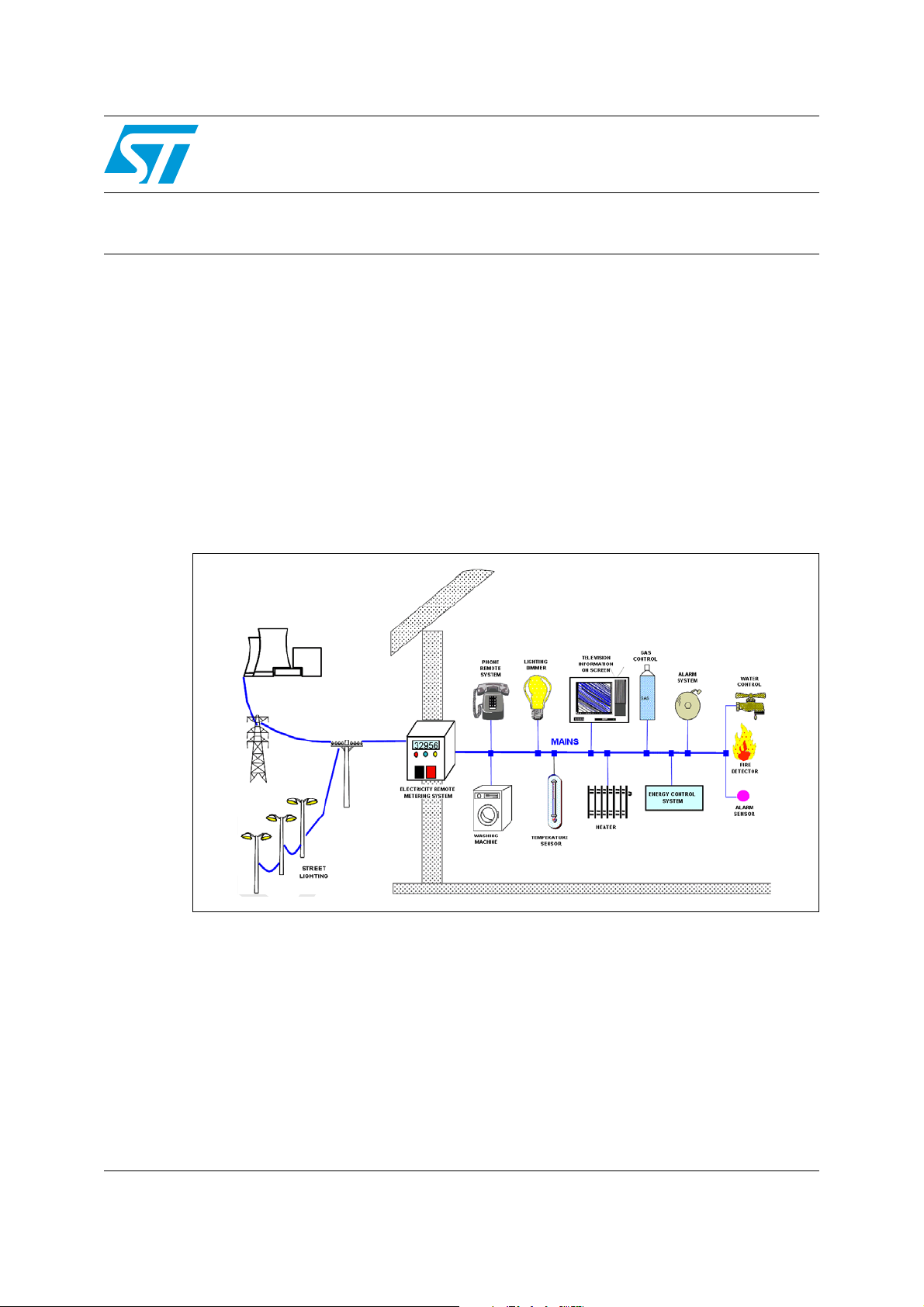
structure, outside the house or in industrial applications (see Figure 1 below).
Figure 1. Typical powerline modem applications scenario
For example in houses or commercial buildings possible applications are power
management, lighting control, heating or cooling system management, remote control of
appliances (by internet or telephone), and control of alarm systems.
Considering external applications, the main areas concern communication with meters, in
particular automatic measuring and remote control, prepaid supply systems, meter or inhome remote displays. Another relevant industrial segment could be street lighting
management.
February 2008 Rev 4 1/46
www.st.com
Page 2

Contents AN1714
Contents
1 Powerline communication . . . . . . . . . . . . . . . . . . . . . . . . . . . . . . . . . . . . 5
1.1 The electrical network . . . . . . . . . . . . . . . . . . . . . . . . . . . . . . . . . . . . . . . . 6
1.1.1 Impedance of powerlines . . . . . . . . . . . . . . . . . . . . . . . . . . . . . . . . . . . . . 7
1.1.2 Noise . . . . . . . . . . . . . . . . . . . . . . . . . . . . . . . . . . . . . . . . . . . . . . . . . . . . 7
1.1.3 Typical connection losses . . . . . . . . . . . . . . . . . . . . . . . . . . . . . . . . . . . . 8
1.1.4 Standing waves . . . . . . . . . . . . . . . . . . . . . . . . . . . . . . . . . . . . . . . . . . . . 8
1.2 ST7538Q FSK powerline transceiver description . . . . . . . . . . . . . . . . . . . . 9
2 Demonstration board for ST7538Q . . . . . . . . . . . . . . . . . . . . . . . . . . . . 11
2.1 Main features . . . . . . . . . . . . . . . . . . . . . . . . . . . . . . . . . . . . . . . . . . . . . . 11
2.2 Signal coupling interface . . . . . . . . . . . . . . . . . . . . . . . . . . . . . . . . . . . . . 13
2.2.1 Transmitting section . . . . . . . . . . . . . . . . . . . . . . . . . . . . . . . . . . . . . . . . 15
2.2.2 Receiving section . . . . . . . . . . . . . . . . . . . . . . . . . . . . . . . . . . . . . . . . . . 18
2.2.3 Voltage regulation-current protection loops . . . . . . . . . . . . . . . . . . . . . . 21
2.3 Board power management . . . . . . . . . . . . . . . . . . . . . . . . . . . . . . . . . . . . 24
2.3.1 L6590 regulator . . . . . . . . . . . . . . . . . . . . . . . . . . . . . . . . . . . . . . . . . . . 25
2.3.2 ST7538Q power supply . . . . . . . . . . . . . . . . . . . . . . . . . . . . . . . . . . . . . 26
2.4 Crystal oscillator . . . . . . . . . . . . . . . . . . . . . . . . . . . . . . . . . . . . . . . . . . . . 28
2.5 Burst and surge protections . . . . . . . . . . . . . . . . . . . . . . . . . . . . . . . . . . . 29
2.6 ST7 microcontroller and RS232 interface . . . . . . . . . . . . . . . . . . . . . . . . 30
2.6.1 Modem / microcontroller interface . . . . . . . . . . . . . . . . . . . . . . . . . . . . . 31
2.7 Bill of material . . . . . . . . . . . . . . . . . . . . . . . . . . . . . . . . . . . . . . . . . . . . . . 33
3 Demonstration board characterization . . . . . . . . . . . . . . . . . . . . . . . . . 37
3.1 Conducted disturbance . . . . . . . . . . . . . . . . . . . . . . . . . . . . . . . . . . . . . . 37
3.2 Narrowband conducted interference . . . . . . . . . . . . . . . . . . . . . . . . . . . . 39
3.3 Output impedance . . . . . . . . . . . . . . . . . . . . . . . . . . . . . . . . . . . . . . . . . . 41
4 Design ideas for auxiliary blocks . . . . . . . . . . . . . . . . . . . . . . . . . . . . . 43
4.1 Zero-crossing detector . . . . . . . . . . . . . . . . . . . . . . . . . . . . . . . . . . . . . . . 43
Appendix A Documentation. . . . . . . . . . . . . . . . . . . . . . . . . . . . . . . . . . . . . . . . . . 44
4.2 ST7538Q . . . . . . . . . . . . . . . . . . . . . . . . . . . . . . . . . . . . . . . . . . . . . . . . . 44
2/46
Page 3

AN1714 Contents
4.3 L6590 integrated power supply . . . . . . . . . . . . . . . . . . . . . . . . . . . . . . . . 44
4.4 ST7 microprocessor . . . . . . . . . . . . . . . . . . . . . . . . . . . . . . . . . . . . . . . . . 44
4.5 Surge and burst protections . . . . . . . . . . . . . . . . . . . . . . . . . . . . . . . . . . . 44
5 References . . . . . . . . . . . . . . . . . . . . . . . . . . . . . . . . . . . . . . . . . . . . . . . . 45
6 Revision history . . . . . . . . . . . . . . . . . . . . . . . . . . . . . . . . . . . . . . . . . . . 45
3/46
Page 4

List of figures AN1714
List of figures
Figure 1. Typical powerline modem applications scenario. . . . . . . . . . . . . . . . . . . . . . . . . . . . . . . . . . 1
Figure 2. Mains signals . . . . . . . . . . . . . . . . . . . . . . . . . . . . . . . . . . . . . . . . . . . . . . . . . . . . . . . . . . . . 6
Figure 3. Aggregate European powerline impedance (by Malack and Engstrom). . . . . . . . . . . . . . . . 7
Figure 4. Voltage spectra of a 100 W light dimmer, a notebook PC, a desktop PC, a CFL lamp,
a TLE lamp, all working with a 50 Hz/~220 V supply . . . . . . . . . . . . . . . . . . . . . . . . . . . . . . 8
Figure 5. FSK modulation . . . . . . . . . . . . . . . . . . . . . . . . . . . . . . . . . . . . . . . . . . . . . . . . . . . . . . . . . . 9
Figure 6. ST7538Q transceiver block diagram . . . . . . . . . . . . . . . . . . . . . . . . . . . . . . . . . . . . . . . . . 10
Figure 7. ST7538Q demonstration board . . . . . . . . . . . . . . . . . . . . . . . . . . . . . . . . . . . . . . . . . . . . . 11
Figure 8. Demonstration board layout . . . . . . . . . . . . . . . . . . . . . . . . . . . . . . . . . . . . . . . . . . . . . . . . 11
Figure 9. Demonstration board schematic: microcontroller and PC interface . . . . . . . . . . . . . . . . . . 12
Figure 10. Demonstration board schematic: line coupling interface and power supply . . . . . . . . . . . . 13
Figure 11. Demonstration board ST7538Q powerline interface. . . . . . . . . . . . . . . . . . . . . . . . . . . . . . 14
Figure 12. Demonstration board ST7538Q transmission coupling circuit . . . . . . . . . . . . . . . . . . . . . . 15
Figure 13. Simplified schematic of the transmission filter . . . . . . . . . . . . . . . . . . . . . . . . . . . . . . . . . . 16
Figure 14. Simulated characteristics of the transmission coupling filter. . . . . . . . . . . . . . . . . . . . . . . . 17
Figure 15. Coupling circuit with a 2
Figure 16. Demonstration board ST7538Q receiving circuits . . . . . . . . . . . . . . . . . . . . . . . . . . . . . . . 19
Figure 17. Measured filtering characteristic of the demonstration board at the RAI pin in receive
mode. . . . . . . . . . . . . . . . . . . . . . . . . . . . . . . . . . . . . . . . . . . . . . . . . . . . . . . . . . . . . . . . . . 20
Figure 18. Powerline output characteristics . . . . . . . . . . . . . . . . . . . . . . . . . . . . . . . . . . . . . . . . . . . . . 21
Figure 19. Voltage regulation and current protection components . . . . . . . . . . . . . . . . . . . . . . . . . . . 22
Figure 20. Voltage regulation/current protection loop logic . . . . . . . . . . . . . . . . . . . . . . . . . . . . . . . . . 22
Figure 21. Current protection loop characteristic . . . . . . . . . . . . . . . . . . . . . . . . . . . . . . . . . . . . . . . . . 24
Figure 22. Voltage regulation and current protection feedback signals . . . . . . . . . . . . . . . . . . . . . . . . 24
Figure 23. Power supply EMC disturbances filter circuit . . . . . . . . . . . . . . . . . . . . . . . . . . . . . . . . . . . 26
Figure 24. Noise generation in resistive supply or ground path . . . . . . . . . . . . . . . . . . . . . . . . . . . . . . 27
Figure 25. A recommended oscillator section layout for noise shielding . . . . . . . . . . . . . . . . . . . . . . . 28
Figure 26. Common mode and differential mode spikes example . . . . . . . . . . . . . . . . . . . . . . . . . . . . 29
Figure 27. Microcontroller/RS232 interface . . . . . . . . . . . . . . . . . . . . . . . . . . . . . . . . . . . . . . . . . . . . . 30
Figure 28. ST7538Q / microcontroller interface . . . . . . . . . . . . . . . . . . . . . . . . . . . . . . . . . . . . . . . . . . 32
Figure 29. Conducted disturbance setup . . . . . . . . . . . . . . . . . . . . . . . . . . . . . . . . . . . . . . . . . . . . . . . 37
Figure 30. Output signal spectrum, channel 132.5 kHz, mains 220 V~, fixed tone . . . . . . . . . . . . . . . 38
Figure 31. Output signal spectrum, channel 132.5 kHz, mains 220 V~, random sequence . . . . . . . . 38
Figure 32. Output signal spectrum, channel 132.5 kHz, mains 110 V~, random sequence . . . . . . . . 39
Figure 33. Output signal spectrum, channel 110 kHz, mains 220 V~, random sequence . . . . . . . . . . 39
Figure 34. Narrowband conducted interferences setup . . . . . . . . . . . . . . . . . . . . . . . . . . . . . . . . . . . . 40
Figure 35. Signal/noise ratio for the 132.5 kHz channel, signal level 85 dBuV . . . . . . . . . . . . . . . . . . 40
Figure 36. Signal/noise ratio for the 132.5 kHz channel, signal level 85 dBuV, mains 110 V~ . . . . . . 41
Figure 37. Signal/noise ratio for the 110 kHz channel, signal level 91 dBuV. . . . . . . . . . . . . . . . . . . . 41
Figure 38. Output board impedance measurement setup . . . . . . . . . . . . . . . . . . . . . . . . . . . . . . . . . . 42
Figure 39. Output demonstration board impedances (CN1) in receiving condition . . . . . . . . . . . . . . . 42
Figure 40. Output demonstration board impedances (CN1) in transmitting condition . . . . . . . . . . . . . 42
Figure 41. Zero-crossing coupling circuit, nonisolated solutions . . . . . . . . . . . . . . . . . . . . . . . . . . . . . 43
Figure 42. Zero-crossing coupling circuit, isolated solutions . . . . . . . . . . . . . . . . . . . . . . . . . . . . . . . . 43
nd
order band pass butterworth . . . . . . . . . . . . . . . . . . . . . . . . . . . 18
4/46
Page 5

AN1714 Powerline communication
1 Powerline communication
Although the concepts of power line communication and home automation, as well as the
development of different devices dedicated for power line communication, have been
present for several years, the market segment for this kind of application has only recently
been growing.
The three main factors that have contributed up to now to the field of the powerline
communication are:
a) The slow development of international norms and standards
b) Some technical constraints related to the electrical network
c) General consideration of costs
The first point concerns standards and norms. A general consideration in an open
communication system is to have mandatory rules and guidelines to guarantee that every
node, whatever the manufacturer, does not compromise the characteristics of the entire
network and the performance of the communication system.
For residential products this aspect is quite relevant considering the presence of many
different appliances and manufacturers, and also the concern for a common language (the
protocol) which is mandatory.
In 2002 the CENELEC (European Committee for Electrotechnical Standardizations)
published or updated a series of regulations about communication on low-voltage electrical
installations. We refer in particular to the EN50065-1, concerning general requirements,
frequency bands and electromagnetic disturbances; the EN50065-4-2 about the low-voltage
decoupling filter and safety requirements; and the EN50065-7 about the impedance of the
devices.
A preliminary version (1999) of the EN50065-2-1 about immunity requirements is also
available.
There has been a certain alignment among the appliance manufacturers on the EHS
(European Home System) protocols, even if a lot of customized protocols are present,
mainly in proprietary mains. More information on EHS protocol is available in the EHS
booklet.
The second critical consideration concerns the technical problems regarding the specific
topology of the electrical network.
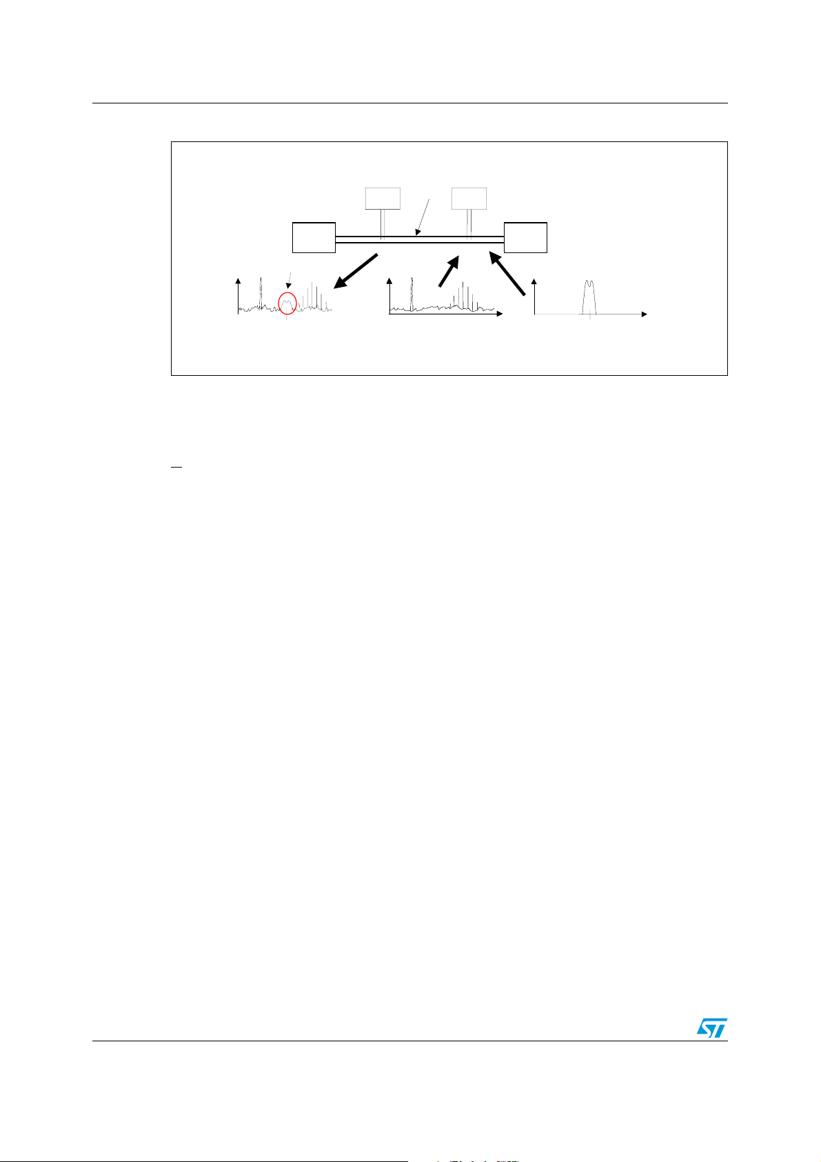
Figure 2 shows what happens to a signal transmitted on an electrical network. For several
reasons that are listed in the next paragraph (low impedance, different kind of disturbances,
etc.) the received FSK signal has a very low level and it is mixed with a great level of noise.
5/46
Page 6
Powerline communication AN1714
Figure 2. Mains signals
MAINS
Tx Rx
ST 7538
ST 7538
ST 7538
ST 7538
Received Signal
fc
f
f f f f
Transmitted Signal
fc
f
f
The aspects of noise and low impedance are more critical in a residential house where
many different appliances are present.
Every entity of the network has to be able to manage reliable communication also under
these critical conditions. To achieve this goal all aspects of the application design have to be
to
carefully considered, from the coupling interface to the power management, from the type
of microprocessor to the powerline transceiver, as well as considering their mutual
influences.
Last but not least, we must consider the economic point of view. It isn’t a simple calculation
of the node cost with respect to an equivalent wireline or wireless solution, but a
consideration of other aspects such as the installation and configuration cost of the entire
network.
Another economic issue that has to be considered is the power consumption of a single
communication node. The power consumption of each communication unit has to be lower
as possible because every unit must always stay on ready to receive commands from a
remote transmitter. This constraint is even more relevant in applications with a huge number
of nodes. Consider for example the control of a street lighting system with thousands of
lamps or a metering system with several thousands of electricity meters.
The ST7538Q has been designed considering all issues previously listed. With this device it
is possible to obtain highly efficient and reliable applications for powerline communication,
characterized by low power consumption, low cost, and compliance with the main norms
and protocol currently in place.
1.1 The electrical network
The communication medium consists of everything connected to power outlets. This
includes house wiring in the walls of the building, appliance wiring, and the appliances
themselves, the service panel, the triplex wire connecting the service panel to the
distribution transformer and the distribution transformer itself. Since distribution transformers
usually serve more than one residence, the loads and wiring of all residences connected to
the same transformer must be included.
6/46
Page 7
AN1714 Powerline communication
1.1.1 Impedance of powerlines
A powerline has very variable impedance depending on several factors such as its
configuration (star connection, ring connection) or the number of entities linked.
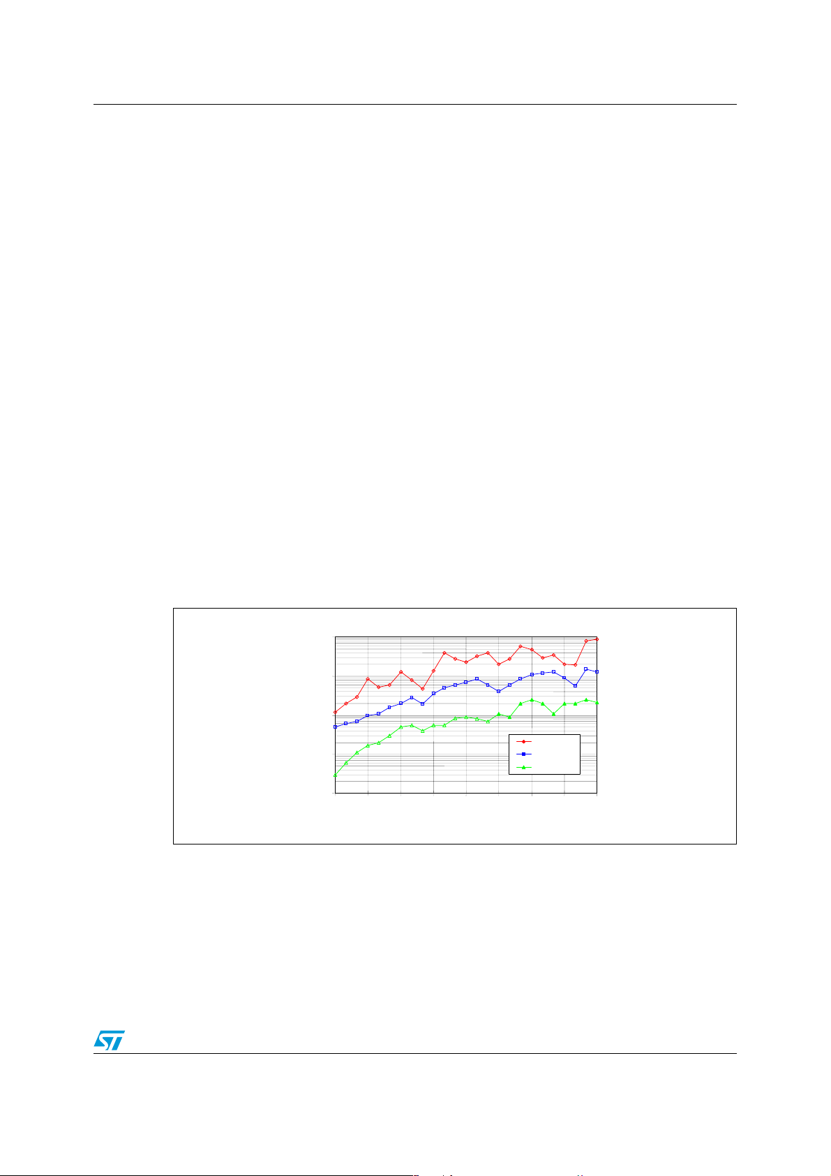
Extensive data on this subject has been published by Malack and Engstrom of IBM
(Electromagnetic Compatibility Laboratory), who measured the RF impedance of 86
commercial AC power distribution systems in six European countries (see Figure 3).
These measurements show that the impedance of the residential power circuits increases
with frequency and is in the range from about 1.5 to 8 Ω at 100 kHz. It appears that this
impedance is determined by two parameters - the loads connected to the network and the
impedance of the distribution transformer. Recently a third element influences the
impedance of the powerline, in particular in residential networks. It is represented by the
EMI filters mounted in the last generation of home appliances (refrigerators, washing
machines, television sets, stereos). Wiring seems to have a relatively small effect. The
impedance is usually inductive.
For typical resistive loads, signal attenuation is expected to be from 2 to 50 dB at 150 kHz
depending on the distribution transformer used and the size of the loads. Moreover, it may
be possible for capacitive loads to resonate with the inductance of the distribution
transformer and cause the signal attenuation to vary wildly with frequency.
For the compliance tests the normative EN50065 use two artificial mains networks
conforming to sub clause 11.2 of CISPR 16-1:1993. Measurements on real networks have
shown that this artificial network does not truly represent practical network impedance. To
better evaluate the performance of a real signaling system, an adaptive network must be
used in conjunction with the CISPR 16-1 artificial network. The design of the adaptive circuit
is included in the informative annex F of EN50065-1 (revision 2001).
Figure 3. Aggregate European powerline impedance (by Malack and Engstrom)
1.1.2 Noise
Appliances connected to the same transformer secondary to which the powerline carrier
system is connected cause the principal source of noise. The primary sources of noise are
Triacs used in light dimmers, universal motors, switching power supplies used in small and
portable appliances and fluorescent lamps.
IMPEDANCE MAGNITUDE (OHM)
1000.0
100.0
10.0
MAXIMUM
1.0
0.1
0.04 0.08 0.10 0.30 0.75 2.10 5.00 15.00 30.00
FREQUENCY (MHz)
MEAN
MINIMUM
7/46
Page 8
Powerline communication AN1714
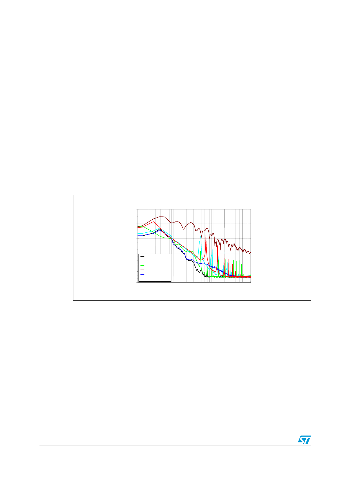
Triacs generate noise synchronous with the 50 Hz power signal and this noise appears as
harmonics of 50 Hz. Universal motors found in mixers or drills also create noise, but it is not
as strong as light dimmer noise, and not generally synchronous with 50 Hz.
Furthermore, light dimmers are often left on for long periods of time whereas universal
motors are used intermittently.
In the last years two other sources of strong noise have been introduced in the electrical
network. They are Compact Fluorescent Lamps (CFL) and the switching power supplies of
rechargeable battery (for example notebook PCs) or small appliances.
In many cases they have a working frequency or some harmonics in the range of the
powerline communication band (from 10 kHz to 150 kHz). Of course the presence of
continuous tones exactly at communication channel frequency can affect the reliability of
communication.
The Figure 4 shows some of the noise sources we refer to. The measurement setup
consists of an insulation transformer with a VARIAC, a spectrum analyzer HP4395A coupled
by a high voltage capacitor (1µF) and a 2 mH transformer (1:1).
Figure 4. Voltage spectra of a 100 W light dimmer, a notebook PC, a desktop PC, a
CFL lamp, a TLE lamp, all working with a 50 Hz/~220 V supply
dBuV
110.0
90.0
70.0
50.0
30.0
10.0
Background
CFL 11W
Desktop PC
Dimmer 100W
TLE 22W
Notebook PC
1.00E+03 1.00E+04 1.00E+05 1.00E+06
1.1.3 Typical connection losses
The transmitting range of a home automation system depends on the physical topology of
the electric power distribution network inside the building where the system is installed.
Different connection losses can be measured. For communication nodes connected to the
same branch circuit from transmitter to receiver a typical connection loss is about 10-15 dB.
If transmitter and receiver are in different branches of the circuit, separated for example by a
service panel, there is an additional attenuation of 10-20 dB.
In some worst-case conditions (socket with very low impedance) the attenuation of the
transmitted signal can reach a value of 50-60 db.
Hz
1.1.4 Standing waves
Standing wave effects begin to occur when the physical dimensions of the communication
medium are similar to about one-eighth of a wavelength, which are about 375 and 250
8/46
Page 9
AN1714 Powerline communication
meters at 100 and 150 kHz respectively. Primarily the length of the triplex wire connecting
the residences to the distribution transformer determines the length of the communication
path on the secondary side of the power distribution system. Usually, several residences
use the same distribution transformer. It would be rare that a linear run of this wiring would
exceed 250 meters in length although the total length of branches might occasionally
exceed 250 meters. Thus standing wave effects would be rare at frequencies below 150 kHz
for residential wiring.
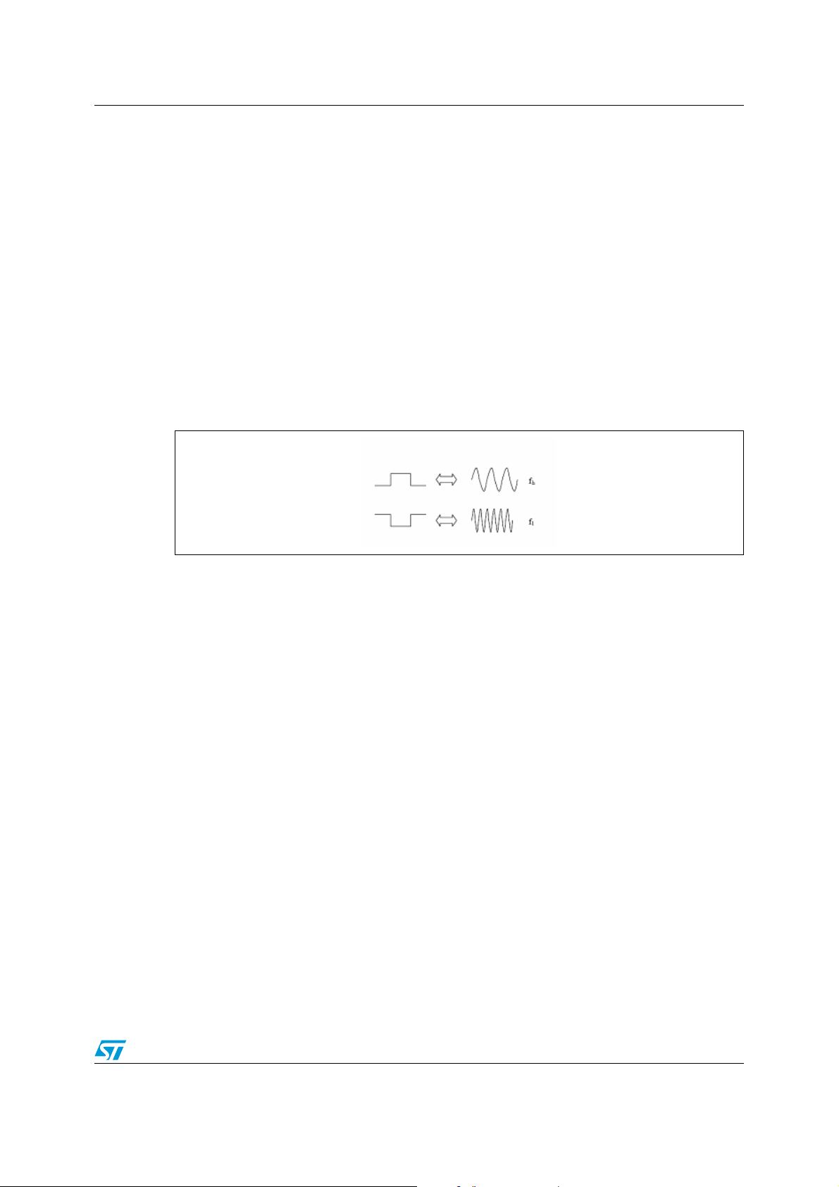
1.2 ST7538Q FSK powerline transceiver description
The ST7538Q transceiver performs a half-duplex communication over the powerline
network using Frequency Shift Keying (FSK) modulation. The FSK modulation technique
translates a digital signal into a sinusoidal signal that can have two different frequency
values, one for the high logic level of the digital signal (f
(f
), as depicted in Figure 5.
L
Figure 5. FSK modulation
), the second one for the low level
H
The average value of the two tones is the carrier frequency (f
). The difference or distance
C
between the two frequencies is a function of the baud-rate (BAUD) of the digital signal (the
number of symbols transmitted in one second) and of the deviation (dev). The relationship
is:
Equation 1
fHfL– BAUD dev–=
The ST7538Q can be programmed to communicate using eight different frequency
channels (60, 66, 72, 76, 82.05, 86, 110 and 132.5 kHz), four baud rates (600, 1200, 2400
and 4800 symbols per second) and two frequency deviations (1 and 0.5).
The device operates from a 7.5 to 12.5 V single supply voltage (PAVcc) and integrates a
differential-output PowerLine Interface (PLI) stage and two linear regulators providing 5 V
(VDC) and 3.3 V (DVdd).
Many auxiliary functions are integrated. The transmission section includes automatic control
on PLI output voltage and current, programmable timeout function and thermal shutdown.
The reception section includes automatic input level control, carrier/preamble detection and
band-in-use signaling.
Additional features are included, such as a watchdog timer, zero-crossing detector, internal
oscillator and a general purpose op-amp.
The serial interface (configurable as UART or SPI) allows interfacing to a host
microcontroller, intended to manage the communication protocol. A reset output (RSTO)
and a programmable 4-8-16 MHz clock (MCLK) can be provided to the microcontroller to
simplify the application.
9/46
Page 10
Powerline communication AN1714
Communication on the powerline can be either synchronous or asynchronous with the data
clock (CLR/T) provided by the transceiver at the programmed baud rate.
When in Transmission mode (i.e. RxTx line at low level), the ST7538Q transceiver samples
the data on the TxD line, generating an FSK modulated signal on the ATO pin. The same
signal is fed into the differential power amplifier to get four times the voltage swing and a
current capability up to 370 mA rms.
When in Reception mode (i.e. RxTx line at high level), an incoming signal at the RAI line is
demodulated and converted in a digital bit stream on the RxD pin.
The internal Control Register, which contains the operating parameters of the ST7538Q
transceiver, can be programmed only using the SPI interface. The Control Register settings
include the Header Recognition and Frame Length Count functions, which can be used to
apply byte and frame synchronization to the received messages.
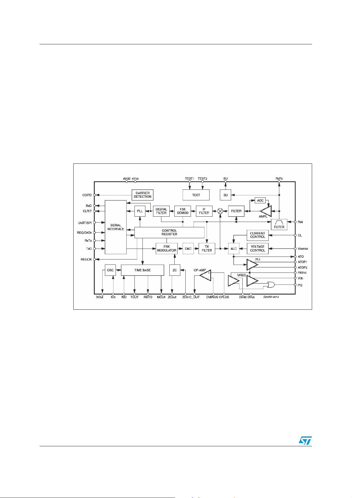
Figure 6. ST7538Q transceiver block diagram
For a more detailed and complete description of the ST7538Q device please refer to the
product datasheet.
10/46
Page 11
AN1714 Demonstration board for ST7538Q
2 Demonstration board for ST7538Q
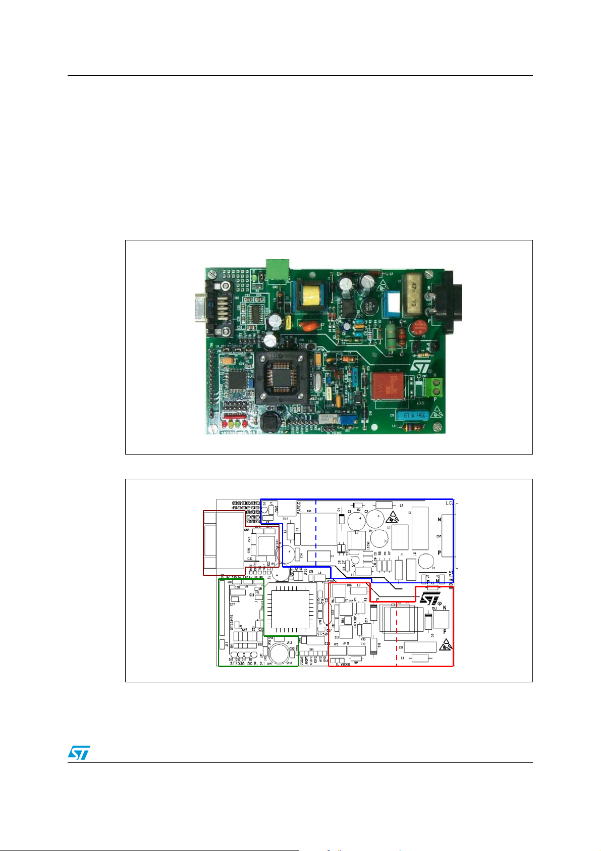
2.1 Main features
The ST7538Q demonstration board implements in a two layer PCB a complete powerline
communication node, including the powerline coupling circuits, a power supply section, a
microcontroller and a RS232 serial interface to connect the board to a personal computer
(Figure 8). This board with the related firmware load in the ST microprocessor and the PC
software is a complete reference for the mains aspects of powerline communications.
Figure 7. ST7538Q demonstration board
Figure 8. Demonstration board layout
LV HV
LV HVLV HV
LV
LV
Power Supply
Power Supply
PC Interface
PC Interface
Q
ST7538P
ST7
ST7
The aim of this board is to give a useful tool to develop and to evaluate a powerline
application with the device ST7538Q. So even if aspects of the board concerning size and
cost aren't optimized, its schematic gives a good design reference and a valid starting point
ST7538P
LV
LV
Signal Coupling
Signal Coupling
Interface
Interface
LV HV
LV HV
11/46
Page 12
Demonstration board for ST7538Q AN1714
to develop powerline modem applications. Moreover the board structure (a lot of jumpers,
test points, few SMD components) allows easily connecting test probes to take measures
and signal verifications, as well as customizing the application according to specific
requirements.
Figure 9. Demonstration board schematic: microcontroller and PC interface
TXD
D13
1N4148
MICRO_TXD
H_S
RS232_OUT
RS232_IN
R1IN_A
T1OUT_A
5V_232
C24 100nF C23 100nF
5V_ P
RESET
RS232_OUT
MCLK
ISPSEL
PA7
PA6
PA5
PA4
RS232_IN
SS
CLRT
TOUT
REG_OK
H_S
WD
REG/DATA
RXTX
ZCOUT
PG
JP1
R2OUT
T2IN
T1IN
R1OUT
R1IN
T1OUT
VCC
GND
OSCOUT
VDD_2
RESET
PE0/TD0
OSCIN
ISPSEL
(HS)PA7
(HS)PA6
(HS)PA5
(HS)PA4
PE1/RDI
ANI0/PD0
ANI3/PD3
ANI4/PD4
ANI5/PD5
MCO/PF0
PB0
PB1
PB2
PB3
VDDA
PF2
VSSA
R16
4.7K
9
10
11
ST232
12
13
14
16
15
5V_ P
C28
C29
C30
C27
100nF
R2IN
T2OUT
C2-
C2+
C1-
C1+
V-
100nF
T2OUT_A
C26
100nF
C25
100nF
C32
100nF
100nF
U3
8
7
5
4
3
1
6
2
V+
10 F
CN5
FEMALE
PC INTERFACE
5
9
4
8
3
7
2
6
1
C31
100nF
R1IN_A
T1OUT_A
T2OUT_A
5V
RN1
1
5
4
3
2
TOUT
U4
VDD_1
41
43
39
44
42
38
37
36
35
34
1
2
3
4
5
7
10
11
12
13
17
15
14
ST2334N2
32
PA3
31
PC7/SS
30
PC6/SCK/ISPCLK
29
PC5/MOSI
28
PC3/ICAP1_B(HS)
26
PC4/MSO/ISPDATA
27
PC2/ICAP2_B(HS)
25
PC1/OCMP1/B
24
PC0/OCMP2/B
23
EXTCLK_A(HS)
20
ICAP1_A/PF6(HS)
19
OCMP1_A/PF4
18
PF1/BEEP
16
AN2/PD2
9
AN1/PD1
8
PB4
6
VDD_0
21
VSS_0
22
VSS_1
33
VSS_2
40
5V_ P5V_ P
CN7
21
3
4
5
6
7
8
10
9
ISP INTERFACE
COMMON
R4
R3
R2
R1
D11
D10
RED
YELLOW
CD/PD
PA4 PA5 PA6 PA7
5V
5V_ P
CD/PD
SS
ISPCLOCK
CLRT
J11
RXD
ISPDATA
MICRO_TXD
BU
5V_ P
D03IN1450
5V_led
RX
J10
J9
J8
CN6
R17
10K
12
11
10
7
6
4
8
3
5
9
2
1
ISPDATA
ISPCLOCK
RESET
ISPSEL
D12
GREEN
5V_232
5V_led
5V_ P
D9
RED
TX
12/46
Page 13
AN1714 Demonstration board for ST7538Q
Figure 10. Demonstration board schematic: line coupling interface and power
supply
P
2
5.1Ω
ATOP2
VDCAVDDTEST1
N.C.
N
J4
J5
4096-X046
VAC T60403-
D16
P6KE6V8A
C13 220nF
50K
R12
TRIM
VSENSE
ATOP1
RXFO29TEST2
19
31
21
332835
17
3
37
1
RXD
CD/PD
CPLUS
CMINUS
RXD
CD/PD
J2
J6
CL
VSENSE
D03IN1451
C36
4.7nF
L7
330H
750
R11
P10V
C38
10 F
1K
R14
C17
5.6nF/63V
C21
100nF
JPTIN
AVSS25PAVCC22PAVSS
GND
6
30
Q
ST7538P
5
42
4
40
C_OUT
C_OUT
J3
RxTx
Rx/Tx
TXD
5V
REG_OK
TXD
36
PG
REG_DATA
PG
REG_OK
38
C18 47pF
XIN
20
U2
43
12
RSTO
R15 4.7K
REG/DATA
RESET
C33
10nF
J7
C37
100pF
TO GND
C19 18pF
SOLD CRYSTAL CASE
ZCOUT
1x
16MHz
ZCOUT
RAI
XOUT
15
32
27
26
10
2
41
18
GND
DVSS
DVSS
DVDD
SW1
C20
C22
22nF
300nF
5V
WD
WD
CL
14
7
CLRT
TIMEOUT
TIMEOUT
23
8
CLRT
ATO
BU
ATO
24
13 16
44
34
39
11
9
BU
R13
5K
ZCIN
N.C.
N.C. N.C. TEST3
MCLK
MCLK
TRIM
JP16
JP13
5V
P10V
TR1
4
RADIOHM 69E16H1B
L2 220 H
D1
1.5A W04
C1
47nF
R1 16.2 2W
L5 1mH
P
N
F1 TR5-F 0.5A
1
CN1
CN4
L3 10 H
D2
STPS160ASMA
D3
BZW06-
C3
4.7 F
C2
4.7 F
L1 42V15
400V
2
ACLINE
234
1
ZCIN
CN2
J1
7
D4
171
400V
400V
2 x 10mA
0.3A RADIOHM
AC
to 256V
AC
85V
ZCOUT
1
C5
C4
281
STTA106
DRAIN
ATOP1
R2
470 F
470 F
C34
VCC
1
L6590
ATOP2
2
2.2K
16V
16V
100nF
3
5
C6
GND
RXFO
D5
D6 1N4148
R3 10
6
6
ATO
GREEN
50V
22 F
7
GND
D7 1N4148
R5 3.3K RL6 10
VFB
U1
GND
CN3
1
R8
4.7M
220V X2
C11 33nF
7
L4 22 H
1T1T
T2
D17
SM6T6V8A
D15
P6KE6V8A
R10
C_R9
100nF
LC12 10 H
JP36
3
C15
100nF
1F
C10
R7
58
4
910
C8
VCOMP
1F
C14
10 F
L8
10 H
C16
100nF
5V
JP35
C7
2.2nF/Y1
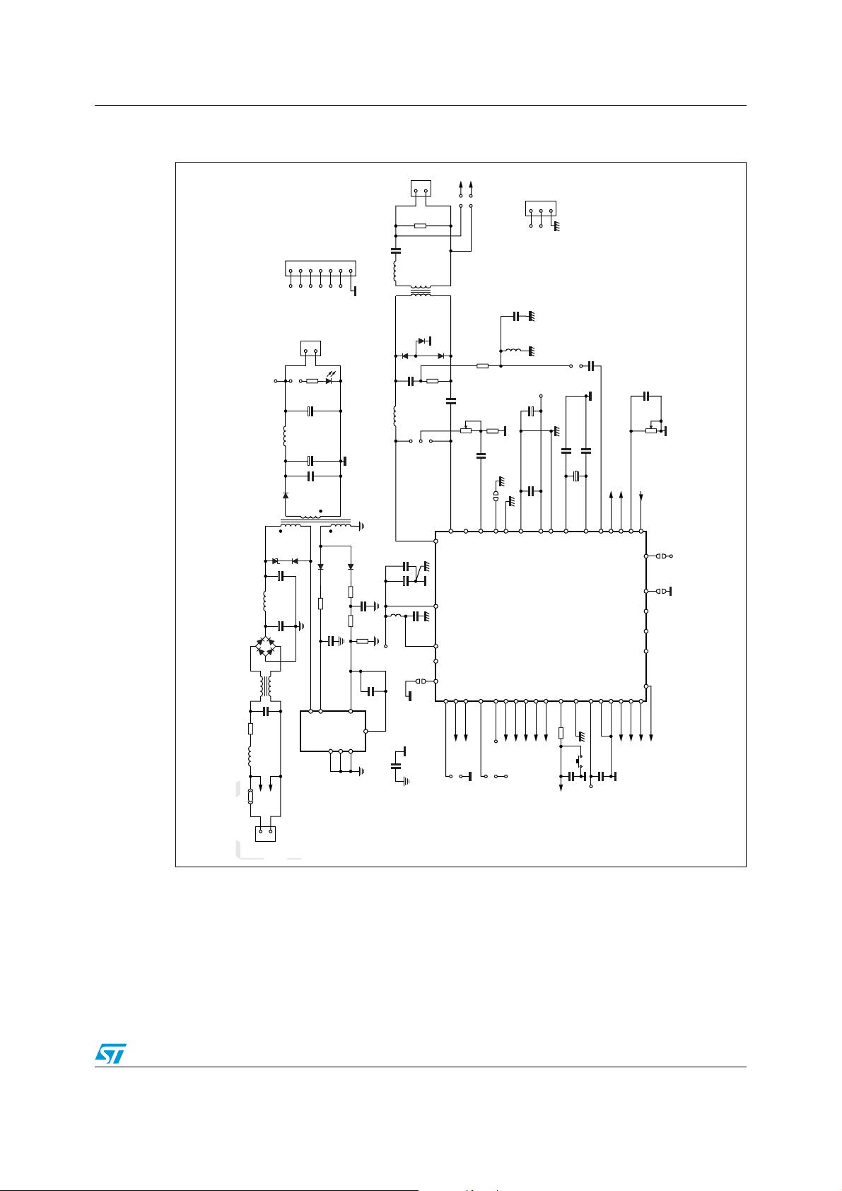
2.2 Signal coupling interface
The line signal interface links the application board to the mains, obtaining a highly efficient
coupling circuit for the received and transmitted FSK signals and a reliable filtering system
for the mains voltage (220 V~/50 Hz or 110 V~/60 Hz), for noise and for bursts or surges.
13/46
Page 14
Demonstration board for ST7538Q AN1714
It is possible to implement different topologies of coupling circuits. A first classification is
between an isolated solution with a line transformer or a double capacitor and a nonisolated
solution with a single high-voltage decoupling capacitor. The last one is simpler and
cheaper, while the first one achieves better performances using efficiently the differential
power output of the devices.
The differential solution has been also preferred for the advantage in reducing the even
harmonics of the transmitted signals.
Figure 11. Demonstration board ST7538Q powerline interface
Q
ST7538
RAI
ATO P1
ATOP2
32
19
21
21
Rx Band Pass Filter
C33
C36
C36
C13
LC12
Tx Band Pass Filter
L7
L7
R11
R10
CR9
D16
D15
Protections
D17
Tx Band Pass Filter
1:1
1:11:1
T1
L4
C11
MAINS
R8
In the design of the coupling interface many technical and standard constraints have to be
considered that are different in a receiving condition with respect to a transmitting status.
Following is a list of design specifications for signal coupling for the European market:
● High selectivity in receiving mode (EN50065-2-1)
● Output impedances as great as possible (EN50065-7)
● Low noise in receiving mode
● Wide voltage and current signal compatibility in every condition (EN50065-1)
● Very low distortion in transmission mode (EN50065-1)
● High coupling efficiency in transmission mode (also with high loads)
● High reliability to burst and surge spikes (EN50065-2-1)
A series of constraints listed in EN50065-4-2, "Low voltage decoupling filters - Safety
requirements", have to be guaranteed by the decoupling elements (transformer or
capacitors) in order to be compliant with a
4 kV or 6 kV class.
The solution implemented in the demonstration board is an isolated circuit with a 1:1
transformer and a X2 class capacitor. In the chosen topology the transmission sections
components do not have any relevant influences on the receiving circuits, so the two
structures can be analyzed separately. The component values that consitute the passive
filters have been dimensioned for the 132.5 kHz channel, but also with the 110 kHz
communication frequency, the performances of the board meet the requirement for reliable
communication.
14/46
Page 15

AN1714 Demonstration board for ST7538Q
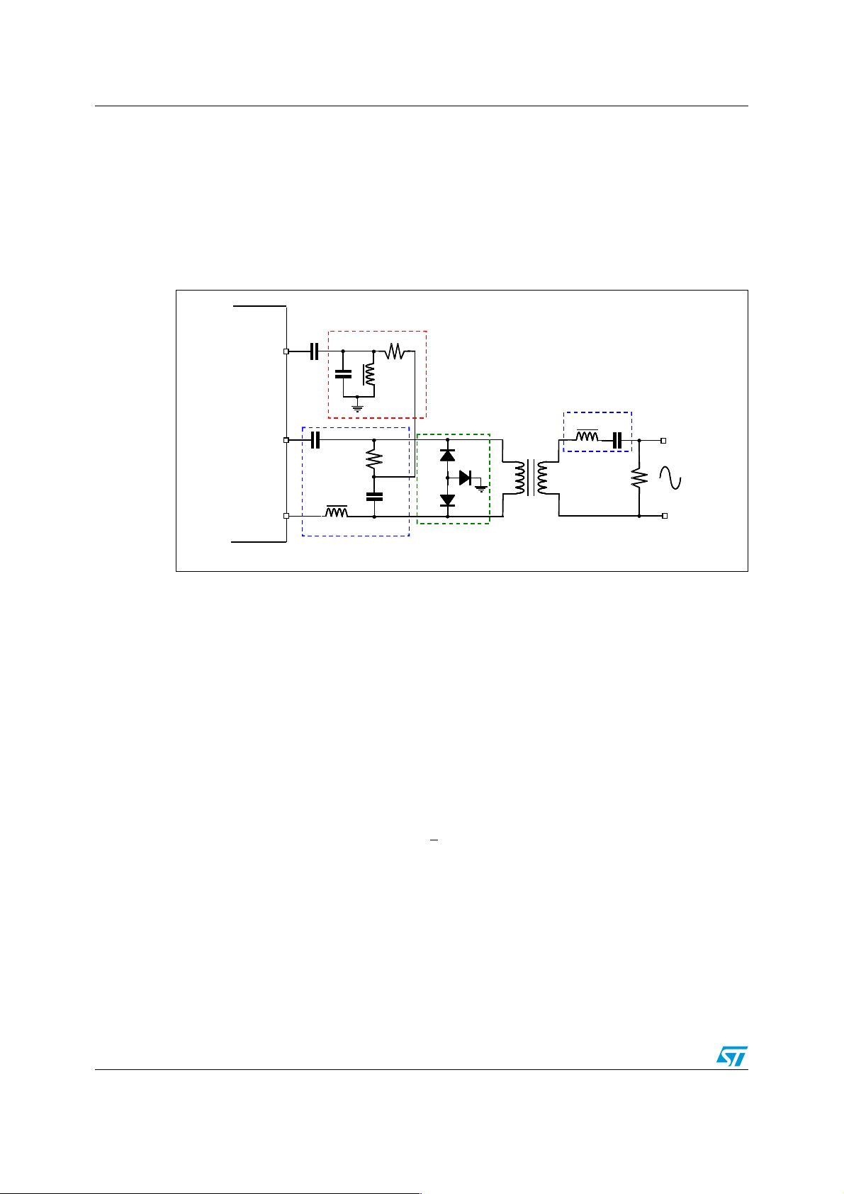
2.2.1 Transmitting section
The function of the transmitting coupling circuits is to inject the transmitted signal coming
from the power amplifiers (ATOP1/ATOP2) to the mains with the maximum efficiencies and
filter noise and spurious signals over the Cenelec mask (EN50065-1, section 7:
disturbances limits).
The critical frequencies of the conducted disturbances emitted are the 2
harmonics of the transmitted signal (265 kHz and 497.5 kHz for the channel at 132.5 kHz)
the harmonics of the working frequency of the power supply regulator and two spurious
tones centered at 1.3 MHz (+/- the channel frequency) produced by the direct synthesis
technique used for the transmitted signal generation.
The configuration used for the transmitted circuit uses a 4th order band pass filter (four
poles and two zeros). In order to have good immunity to the components spread (accuracy
and temperature) and to the load variation, the filter has a band of about 60 kHz (see
Figure 14). To obtain this characteristic two poles can be put at a frequency of about 100
kHz and the other at a frequency of about 160 kHz.
Figure 12. Demonstration board ST7538Q transmission coupling circuit
nd
and 3rd
100K
ST7538
RAI
Ω
2.5V
ATOP1
ATOP2
Q
C33
C33
32
32
C36
C36
19
19
C13
21
21
LC12
L7
L7
R10
CR9
R11
R11
Transmission
Coupling Section
D16
D15
D17
Artificial Network
C11
R8
R8
CISPR 16-1
Ω
Ω
50
50
Ω
Ω
50
50
L4
1:1
1:1 1:1
T1
T1
µ
µ
H
H
50
50
Ω
Ω
5
5
Ω
Ω
5
5
µ
H
50
For a correct dimension of the filters the mutual influence of the various components has to
be considered, as well as the influences due to the other elements: the leakage inductance
of the transformer (from 0.1 µH to 10 µH), the capacitance of the transil diode (about 2 nF),
the ESR of the series components C
, LC12, T1, L4, C11 (from 100 mΩ to 1 Ω).
13
For a first approximate rate of the components’ values, only the reactive components are
used in the simplified circuit of Figure 13 and the transformer (1:1 ratio) is considered ideal.
For the correct dimensioning of the filter it is better to consider the typical impedances
expected for the mains network (usually an inductive load). If an impedance characterization
of the network is not available it is possible to use a reference load like the artificial network
CISPR16-1 (50 ohms parallel 5 Ω plus 50 µH). In the simplified circuit only the reactive part
of the CISPR 16 artificial network (2 x Lc = 100 µH) has been considered
15/46
Page 16

Demonstration board for ST7538Q AN1714
Figure 13. Simplified schematic of the transmission filter
CISPR
C13
1
st
Loop
LC12
CR9
CR9
L4
C11
nd
2
Loop
Load
L
L
L
c
c
c
c
= 50
= 50
= 50
H
µ
H
H
µ
µ
The formulas for the two couples of poles are:
Equation 2
ƒ
p1ƒp2
------------------------------------------------------- -
2 π L
1
⋅⋅⋅
C12CA
160k Hz ƒ
p2ƒp3
------------------------------------------------
2 π LBCB⋅⋅⋅
1
100k Hz≅≅=,≅≅=
Equation 3
1
13
;+
1
------------ -
C
B
1
------------
C
R9
1
---------- -+==
C
11
--------
C
1
1
---------- -
------------
C
C
A
R9
The peak value of the signal current can reach with heavy load a current peak value greater
than 1 A so all the components of the coupling interfaces in series to the signal (in particular
the inductors LC
, L4 and the transformer T1) have to be guaranteed for this current without
12
saturation or overheating problems. The maximum current of the inductive elements, as well
as the series resistance, are proportional to the value of the inductance.
In any case the ESR of these inductive elements has to be as low as possible to obtain a
good coupling interface. In fact with a global impedance series greater than 2 Ω the coupling
losses of the transmitted signal with heavy loads could be excessive.
For these reasons an LBC (Large Bobbin Core) inductor with values small as possible (L
= 10 µH and L
Another constraint concerns the value of the capacitor C
= 22 µH) has been chosen in this circuit.
4
. This is an X2 class capacitor
11
C12
that has the primary function to uncouple the transformer from the mains. It is better to use a
value as low as possible for economic reasons, as well as to obtain a 50 Hz mains current in
the secondary coil of the transformer as low as possible in order to reduce saturation effects.
The value chosen is 33 nF.
Considering that all the mains voltage drops across the C
capacitor, the current value in
11
the transformer coil is about:
Equation 4
I
Using Equation 2 and Equation 3 the values of C
rms
220V
2 π 50 Hz C11⋅⋅⋅⋅≅ 2.3mA
rms
(100 nF) and C13 (220 nF) can be rated.
R9
=
rms
The requirements for this type of capacitor are accuracy, the temperature compensation and
a low ESR value. Polyester capacitors or polypropylene capacitors (better temperature
coefficient) are suggested. The accuracy should be at least ±10%.
16/46
Page 17

AN1714 Demonstration board for ST7538Q
Figure 14. Simulated characteristics of the transmission coupling filter
VDB (OUTC2)
dB
10
0
-10
-20
-30
-40
-50
-60
-70
-80
1e+U4
1e+U5
Hz
1e+U6
2e+U6
Using components with standard values the real values of the poles are:
Equation 5
ƒ
p1ƒp2
192kHz ƒ
p2ƒp3
91kHz==,==
The values obtained are very close to the spec values and in agreement with the simulated
results (see Figure 14). In any case for a better result we suggest using a simulator or an
equivalent specific program to design filters.
The R
resistor has been added to fit the output impedance requirement in receiving mode
10
(EN50065-7).
An alternative solution for the transmission coupling circuit is shown in Figure 14 above. It
implements a 2nd order band pass Butterworth filter centered at the channel frequency.
The advantage of this solution is the symmetrical structure that compensates the nonlinearity of the components (lower level for the even harmonics).
Also in this case a correct dimension of the filter has to take in account the parasitic
elements of the various components, as well as the load influence.
17/46
Page 18

Demonstration board for ST7538Q AN1714
Figure 15. Coupling circuit with a 2nd order band pass butterworth
ST7538
Transmission 2nd order
Q
Band Pass Butterworth
ATOP1
ATOP2
19
19
220nF
220nF
21
21
220nF
H
H
µ
µ
10
10
100nF
100nF
µ H
10
Ω
Ω
4.7
4.7
H
µ
47
1:1
1:1 1:1
33nF X2
MAINS
One of the most critical components of the application is the signal transformer. In order to
have a good power transfer and to minimize the insertion losses it is recommended a
transformer with a primary inductance greater than 1 mH and a series resistance lower than
0.5 Ω. Another constraint concerns the saturation current: a DC or low frequency current (50
Hz) should be present.
Another parameter to take in consideration is the leakage inductance. If it has a relevant
value (from 10 µH to 50 µH) the inductance L
can be avoided. The drawback is that this
4
parameter has great variation that influences the output filter characteristics. For this reason
in the demonstration board a transformer with a very low leakage inductance (lower than 1
µH) is used .
The European normative (CENELEC) gives another constraint regarding the voltage
insulation resistance and dielectric strength of the application that influences the
transformer. Two classes are indicated, a 4 kV and a 6 kV class. The classification and
measurement criteria are codified in the EN50065-4-2 CENELEC document.
In case of heavy load a smart solution is to use a 2:1 transformer. The equivalent
impedance of the load referred to the primary coils of the transformer has a value four times
bigger than with a 1:1 ratio transformer. Also the current supplied by the power interfaces
has half value. The only critical point is that in order to have the same output signal level on
the mains, the ST7538Q power interfaces has to generate a double signal (more problems
with odd harmonics).
Seldom a low amplitude signal at high frequency (greater than 10 MHz) can be present on
the output signal. It should originate by a resonance from the leakage inductances and the
parasitic capacitance of the board and of the ST7538Q output stage. Usually the series
inductor L
stops this kind of oscillation.
C12
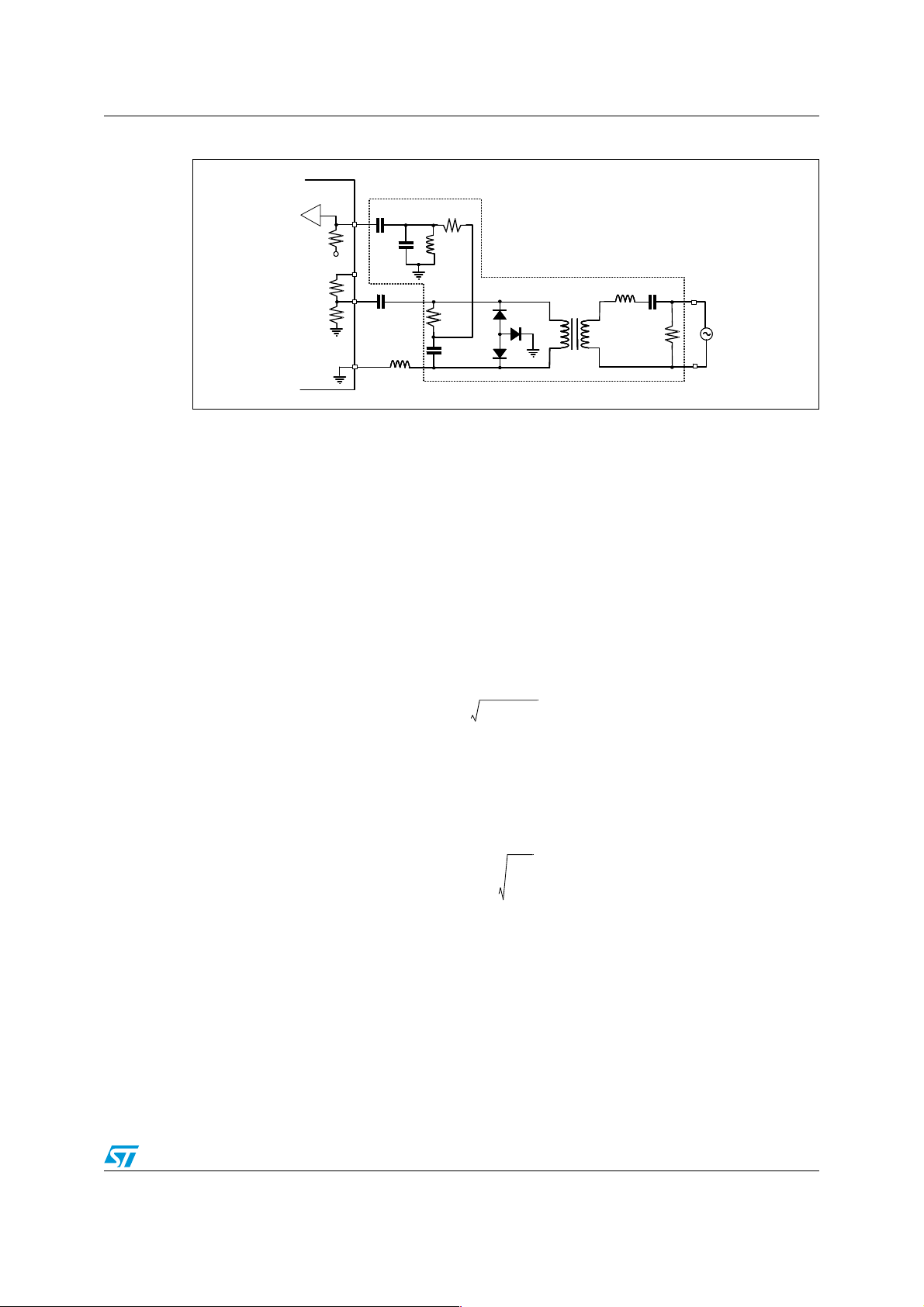
2.2.2 Receiving section
The receiving circuit of the coupling interface has the main function to filter noise tones from
the network that can overcome the maximum absolute rates of the RAI pin, or in any case
degrade the demodulation performances of the device (EN50065-2-1, section 7.2.3:
narrow-band conducted interference).
The solution adopted in the demonstration board consists of a resonant parallel circuit that
implements a 2
component that saves the DC value on the RAI pin (2.5 V). This DC value obtains the
maximum voltage input signal (2Vrms) compatible with the absolute of the devices.
nd
order passive filter (C36, L7 R11). The C33 capacitor is a decouple
18/46
Page 19
AN1714 Demonstration board for ST7538Q
Figure 16. Demonstration board ST7538Q receiving circuits
ST7538
100K
ATOP1
60K
ATOP2
60K
Q
32
22
PAVCC
19
21
C33
C13
C13
C36
LC12
R11
L7
R10
CR9
Receiving
Coupling Section
D16
D15
D17
1:1
1:1
T1
L4
C11
R8
RAI
Ω
2.5V
Ω
Ω
In the receive mode the ATOP1 pin has a high impedance and a DC polarization at PAVcc/2
while the ATOP2 pin is tied to ground internally into the device with a power MOS (few
milliohm resistance). With this configuration the two resonant series L
R
can be considered as first approximation neglected (L4/C11 has the resonance at the
10
channel frequency while the LC
/CR9 has the resonance at an higher frequency). The only
12
, C11 and LC12, CR9,
4
effect of these components is to attenuate the amplitude of the received signal, about 6 dB
with the used values of CR
and R10.
9
According to these considerations the dimension of the input filter frequency depends
mainly on the choice of C
These components implement a 2
36 L7
and R11.
nd
order band pass filter. The center band frequency of
the filter is the channel frequency:
Equation 6
--------------------------------------------------
ƒ
≅ 132.5k Hz=
0
2 π L7C36⋅⋅⋅
1
The other parameter to take in account for the receiving filter design is the Quality factor (Q).
Its value is a tradeoff between the selectivity requirements (high Q values) and the
component and temperature spreads. Using a polypropylene capacitor with a 5% tolerance
and a BC inductor with a tolerance of 10%, a Q value betweens 2 and 3 is acceptable.
Equation 7
C
QR
11
36
---------- -⋅≅ 2.85=
L
7
In order to not influence the transmitting section and to reduce the DC current through the
primary coil of the transformer, the value of R
should be as high as possible. The
11
drawback of a greater value for this resistor is that it produces a higher white noise. A value
of 750 Ω satisfies these opposite requirements for all communication channels. Fixing the
resistor value and using the previous equations, it is possible to rate the values of C
L
.
7
36
and
19/46
Page 20

Demonstration board for ST7538Q AN1714
Ta bl e 1 shows some possible commercial values for these components in reference to
different communication channels.
Table 1. Parallel resonance Rx filter components
Rx filter
C36 L7 F
0
Ch 132.5 kHz 6.8 nF 220 µH 130.1 kHz
Ch 110 kHz 10 nF 220 µH 107.3 kHz
Ch 86 kHz 10 nF 330 µH 87.6 kHz
Ch 82.05 kHz 8.2 nF 470 µH 81.1 kHz
Ch 76 kHz 10 nF 470 µH 73.4 kHz
Ch 72 kHz 22 nF 220 µH 72.3 kHz
Ch 66 kHz 18 nF 330 µH 65.3 kHz
Ch 60 kHz 22 nF 330 µH 59.1 kHz
The resonance frequency of the filter is strictly linked to the spread of these components
and an excessive spread can produce an excessive attenuation on the received signal. The
accuracy of L
and C36 has to be great.
7
For the same reason the Q factor has a relevant part in the design of the Rx filter. Some
application can use more than one communication channel at the same time, in this case
the best choice is to have a resonance frequency at a mean value of used frequencies and
a Q factor not too high.
Figure 17. Measured filtering characteristic of the demonstration board at the RAI
pin in receive mode
0.00E+00
RxFilter
-1.00E+01
-2.00E+01
dB
-3.00E+01
-4.00E+01
-5.00E+01
1.00E+04 1.00E+05 1.00E+06
For the receiving filter a passive solution is preferred to an active filter. The experience has
shown evidence that an active filter introduces white noise comparable with the received
signal level.
Some receiving circuit interfaces, for example with a 2:1 signal transformer, can have a gain
greater than 0dB (unit gain). In this case, if the band-in-use function level of the ST7538Q is
used, an attenuation of the received signal (for example with a resistors divider) is
necessary to have the same level of the signal present on the mains to be compliant with
Cenelec specifications.
20/46
Hz
Page 21

AN1714 Demonstration board for ST7538Q
2.2.3 Voltage regulation-current protection loops
A powerline network requires an appropriate driving circuit able to adapt the output signal
characteristic to the different and low values of the mains impedance.
Figure 18. Powerline output characteristics
V
V
V
V
0
0
I zone
S
S
A
A
m
m
Figure 18 shows the characteristic of a coupling circuit. The characteristic has a range with
constant voltage amplitude of the transmitted signal. When the line impedance has reached
a critical Z
value, corresponding to the maximum power, the amplitude of the output signal
0
is decreased in order to have a constant current.
I zone
i
i
g
g
n
n
a
a
l
l
p
p
i
i
l
l
u
u
t
t
d
d
e
e
V zone
V zone
z
z
0
0
Z
Z0Z
Line load (ohm)
Line load (ohm)
The value of Z
depends mainly on the network impedance, while the maximum value of V0
0
depends on the norm (EN50065-1) and on the maximum current capability of the powerline
interface.
The ST7538Q integrates a control voltage / current protection circuit. It is possible to
program the values of Z
and V0 with external resistors. The R13 trimmer sets the current
0
protection limit and the R14 and R12 trimmers the peak voltage level. The dimension of
these external components influences the design of the coupling interfaces and of the power
management, too. For example all the components in series to the signal (transformer, filter
inductors, decoupling capacitors, fuses) have to guarantee a maximum current or a
saturation current greater than the maximum current programmed with R
, as well as the
13
dimension of the current capability of the power supply. The capacitors on the supply line
have to be chosen according to the programmed current values.
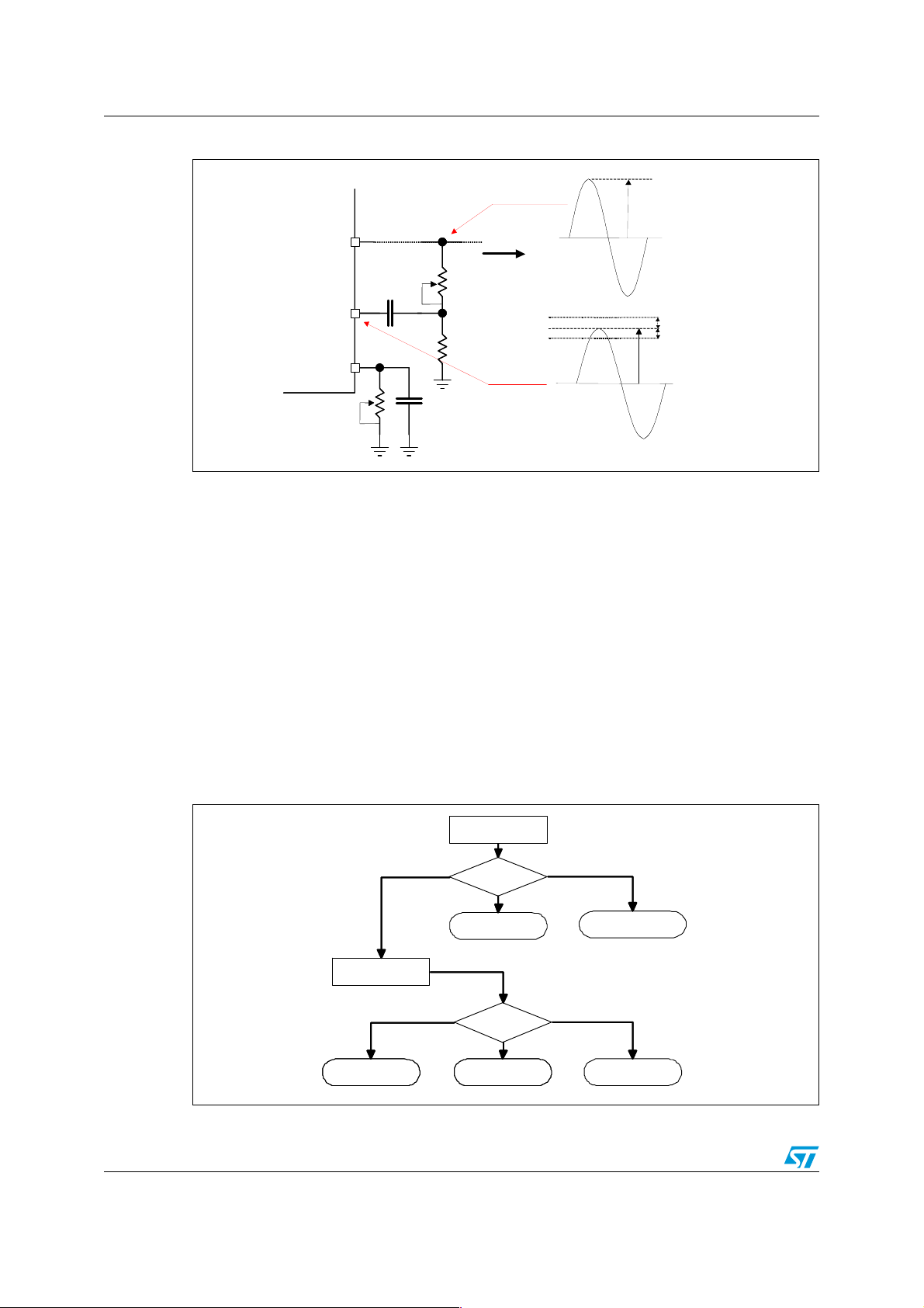
The control loop circuit inside the devices is obtained by a Voltage Controlled Amplifier
(VCA) with a logic circuit that implements the following control (Figure 20). The current
protection has the priority with respect to the voltage loop regulation, so if an output current
greater than the programmed value (I
> IH) is detected, the digital control acts on the VCA
ref
to reduce the output signal voltage. When the current reaches the programmed value, the
gain of the VCA is frozen.
In case of no current protection condition (I
< IL), the voltage regulation loop assumes the
ref
control and modifies the gain of the VCA until the output signal reaches the programmed
values.
The VCA changes its gain at steps of about 1dB (10%). The logic samples the current and
voltages values with an internal clock of 5 Hz, so the transmitted signal is updated every 200
µsec at steps of 1 dB.
21/46
Page 22
Demonstration board for ST7538Q AN1714
Figure 19. Voltage regulation and current protection components
PK
VCL
VCL
Voltage
Controlled
Signal
VCL
VCL
HYST
HYST
VCL
VCL
HYST
HYST
TH
TH
1.865 V
ST7538
ATOP/ATO
VSENSE
CL
Q
Vout
VR
Iout
R
C
17
12
R
14
Signal
Signal
12/R14
pin).
SENSE
C
R
13
37
Feedback
The value of the transmitted signal is programmed using the resistors divider R
capacitor C
has a decoupling function for the DC value on the V
17
The regulations loop changes the VCA amplifier gain until the sinusoidal signal on the
V
±10% (VCL
pin reaches the values of VCLTH (see datasheet values) with a tolerance of about
SENSE
hysteresis value).
HYST
The following simplified formula calculates the resistors divider ratio.
Equation 8
R14R12+
PK
----------------------------
R
14
VCLTHVCL
±()
HIST
VR
For a more precise rate in the formula, the input impedance of the V
VCLTH =190mV
⇒⋅≅
VCL
HIST
=19mV
SENSE
pin (~36 KΩ) and
the decoupling capacitor C17 (for values of some nanofarads this capacitor can be
neglected) have to be considered also.
Figure 20. Voltage regulation/current protection loop logic
Iref < IL
Iref < IL
Current
Current
Control
Control
Test
Test
Iref > IH
Iref > IH
(the
Voltage
Voltage
Control
Control
Increase
Increase
Gain
Gain
22/46
Constant
Constant
Gain
Gain
Test
Test
Constant
Constant
Gain
Gain
Reduce
Reduce
Gain
Gain
Vref > VHVref < VL
Vref > VHVref < VL
Reduce
Reduce
Gain
Gain
Page 23
AN1714 Demonstration board for ST7538Q
In the demonstration board it is possible to link the feedback signal (top of R12 resistor) to
the ATOP1 or to the ATOP2 pin through jumper J36. The choice of the feedback connection
point depends on the network coupling circuit topology.
If a big noise coming from the mains is present disturbing the voltage control loop, a
possible solution is to connect the feedback to the ATO pin. In this case the output signal
has half the value with respect to the ATOP pins, so the R
R
resistor has to be doubled).
14
resistor has a half value (or the
12
In the demonstration board it is possible to change the output signal voltage level acting on
the R
trimmer. Tab le 2 gives the values of the trimmer to assume some standard output
12
values.
Table 2. Voltage regulation loop (divider and R12 resistors values)
V
(Vrms)
out
0.150 103.5 1.1 0.1
0.250 108.0 1.9 0.9
0.350 110.9 2.7 1.7
0.500 114.0 3.7 2.6
0.625 115.9 4.7 3.6
0.750 117.5 5.8 4.7
0.875 118.8 6.6 5.4
(1)
V
(dBuV) (R14+R12)/R
out
14
R12 (KΩ)
(2)
1.000 120.0 7.6 6.4
1.250 121.9 9.5 8.3
1.500 123.5 10.8 9.5
1. The regulated Vout voltage is the point linked to the voltage feedback divider (top of R12).
2. The rate of R14 takes in account the input resistance on the V
(C17) has been neglected.
The resistor connected to the CL pin (the trimmer R
function to program the current protection threshold. The capacitor C
pin (36 KΩ). The decoupling capacitor
SENSE
in the demonstration board) has the
13
in parallel to the
37
resistor has a filtering function for noise and spikes.
A mirrored current (ratio 1:5000) of the p channel power Mos of the powerline interface of
the device (both ATOP1 and ATOP2) is present on the CL pin. The voltage on the CL pin is
proportional to the output current and to the resistor connected to the pin.
The peak value of this voltage is compared with an internal reference of the device. If the
signal overcomes the threshold, the loop acts on the VCA reducing the transmitted signal
and therefore the output current.
The resistor value determines the output signal that the interface is able to supply. In
conjunction with the programmed output voltage V
minimum value of driving impedances (Z
).
0
the maximum current level fixes the
0
23/46
Page 24
Demonstration board for ST7538Q AN1714
Figure 21. Current protection loop characteristic
mA (rms)
350
325
300
275
250
225
200
175
150
125
100
2.0 2.5 3.0 3.5 4.0 4.5 5.0 5.5
Current Protection
R
(Kohm)
13
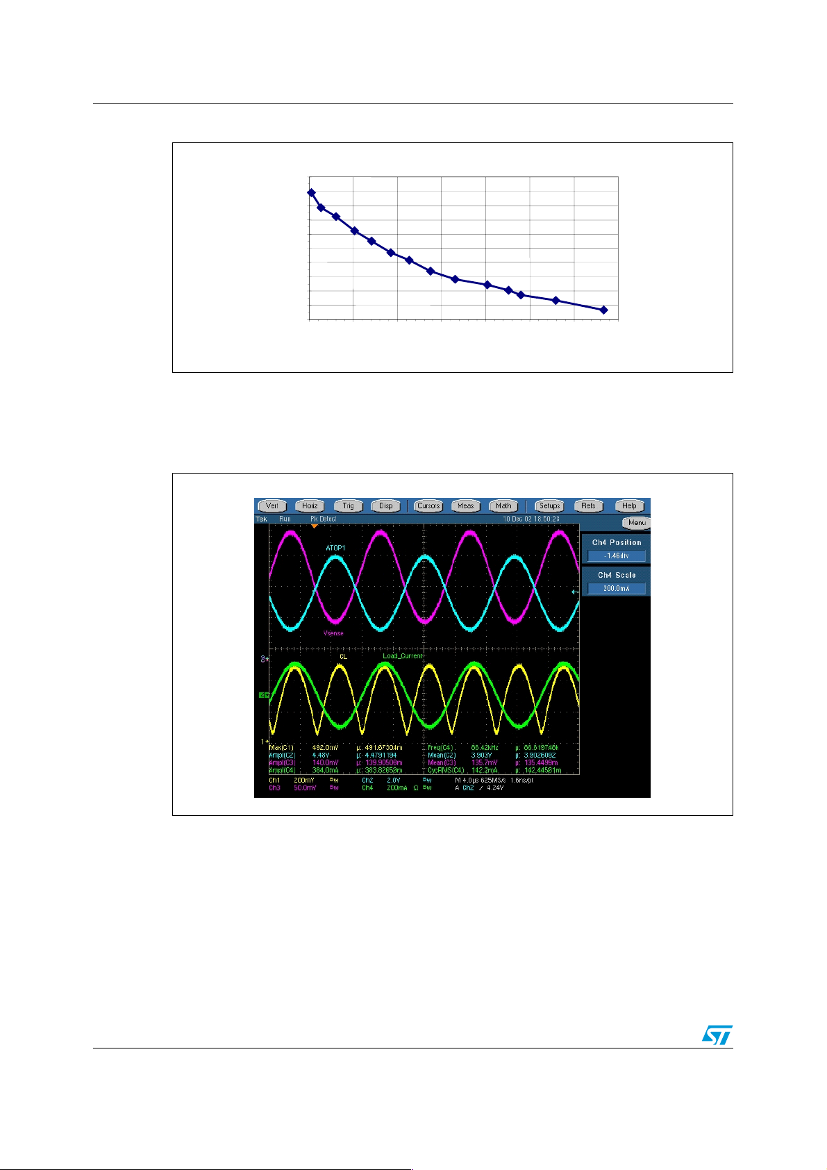
Figure 21 above gives the value of the CL resistor to program the maximum current value.
Figure 22 shows all the main signals of the control loop feedback, i.e. output signal, load
current, V
voltage and CL voltage.
SENSE
Figure 22. Voltage regulation and current protection feedback signals
2.3 Board power management
The demonstration board has a mains supply with a flyback converter using the monolithic
switching regulator L6590. The regulator can have both a 220 V or an 110 V supply voltage
of the mains.
It is possible to use an external power supply connected to CN2, too. In this case the
jumpers J4 and J5 have to be removed and the connector CN3 has to be used instead of the
standard socket CN1.
24/46
Page 25

AN1714 Demonstration board for ST7538Q
The correct supply of the board is indicated by the green LED D5. It is possible to turn off
this LED by removing the J1 jumper.
The 5 V internal regulator of the ST7538Q (VDC pin) supplies the microcontroller ST7, the
ST232 interface device and the LED (D9, D10, D11, D12). Using the jumper connections J8
(ST7), J9 (LEDs) and J10 (ST232) it is possible to monitor the current of these components
or remove the supply to these demonstration board parts.
The 5V supply is available also on pin #1 of the CN6 connector.
A typical power consumption of the powerline application (switched regulator excluded) is
about 18mA in receiving mode, 120 mA in transmitting mode without load. Every LED ON
increases the current consumption by 4 mA.
The current consumption of the RS232 interface is about 12 mA, which means that the
overall current consumption of the microcontroller plus the ST7538Q in receiving mode is
about 6 mA.
The current consumption depends also on the clock frequency selected. There is a variation
of 5 mA from a 4 MHz clock to a 16 MHz clock.
2.3.1 L6590 regulator
The flyback converter configuration using the L6590 regulator has a specific topology that
implements the feedback on an auxiliary winding of the primary side of the flyback
transformer. With this configuration it is possible to save the cost of an optocoupler. The
drawback of this solution is the wide load range of the regulated voltage. In a condition of
low current consumption (20mA) the value of the supply voltage is about 12 V, in
transmission the value is about 10.5V.
The maximum power of this configuration is about 3 W. The dimension of the maximum
power consumption of the regulators is related to the current limit of the powerline interface
programmed with the R13 resistor on the CL pin.
If an external power supply is used, the designer must carefully verify that also in a
continuous transmission condition the supply is able to supply the requested current.
Another aspect that has to be considered with attention in a continuous transmission
condition is the overheating condition of the devices with the thermal protection activation
(transmission aborted and signal TOUT high).
In the demonstration board a socket for the ST7538Q is used, therefore the slug of the
package cannot be soldered to a dissipating surface as recommended. For this reason, in
presence of a heavy load during a continuous transmission, the thermal protection threshold
is reached in a shorter time.
A critical point common to all switching solutions, especially for this kind of application, is the
electromagnetic noise and the conducted disturbance generated. In particular the main
noise frequencies are due to the switching frequency and to the resonance of the leakage
inductance with the drain capacitance.
25/46
Page 26

Demonstration board for ST7538Q AN1714
Figure 23. Power supply EMC disturbances filter circuit
R1
R1
L5
L1
D1
D1
L1
C1
C1
L5
MAINS
MAINS
In the demonstration board these critical values are at 20 kHz or 66 kHz (switching
frequencies respectively with low and high load condition) and at about 800 kHz for the
resonance.
It is important that the resonance of the input filter is at a frequency far from the
communication bands used, otherwise its low impedance attenuates the communication
signals.
For the demonstration board the resonance frequency is from 10 kHz to 20 kHz.
The 15 Ω resistor R1 has the double function to protect the input stage of the supply from
surge or burst and at the same time to make the application board compliant with the
EN50065-7 standard.
Another consideration concerns the frequencies noise generated by the supply. Even if the
noise generated is compliant with the normative mask limit, it is mandatory to choose a
value of switching frequency (and its lower order harmonics) far from the communication
channel frequency. In fact the modem is able to demodulate very low amplitude signals
(500uVrms). Noise, also with a low amplitude value, can degrade the communication.
This consideration is valid only in a receiving condition, during the transmission a little noise
at the same frequency of the transmitted signal (2V
The working frequencies of the L6590 are 20 kHz with a low value current (receiving
condition), and 66 kHz with high current, i.e. in a transmission condition (220 AC MAINS).
In the transmission case the 2
has an irrelevant influence.
The value of the supply voltage is related to the amplitude of the output signal (see the
ST7538Q datasheet), so usually a voltage of at least 10 V is mandatory to avoid distortion
problems. The same voltage value does not occur in a receiving status. In case of strong
constraints regarding the power consumption, it is possible to use two different power supply
values. For example possible values are 10.5 V during the transmission, and 7.5 V in the
receiving status. This can be done easily by changing the feedback resistor divider of the
regulator using a switch controlled by the RxTx signal (pin #4) of the ST7538Q.
For more detailed information about the L6590 and other possible configuration please refer
to the product datasheet and related application notes.
2.3.2 ST7538Q power supply
) can be neglected.
rms
nd
harmonic at 133 kHz (communication channel 132.5 kHz)
A fundamental aspect of the board design is the configuration of the ST7538Q supply
system.
26/46
Page 27

AN1714 Demonstration board for ST7538Q
It is recommended to connect all grounds of the device to a common ground node,
connected to the copper plate of the slug.
During transmission a high current (up to 0.3A
= 0.85App) at the signal frequency is
rms
present through the supply rail and the ground plane. In case of ground or supply paths with
a "high" resistance (even a few mΩ can be critical), the high current could produce a ripple
at the second harmonic of the signal frequency that should be coupled onto the mains:
Equation 9
0.85A
0.002Ω 1.7mV
pp
pp
56dBµV≅=⋅
As the rate above shows, the noise contribution has a relevant value with respect to the
Cenelec mask.
Figure 24. Noise generation in resistive supply or ground path
Noise
Noise
Q
ST7538
ST7538
22
22
PAVcc
PAVcc
ATOP1
ATOP1
19
19
ATOP2
ATOP2
21
21
2mΩ
2mΩ
L
L
Z
Z
PAVss
PAVss
18
18
2mΩ
2mΩ
Noise
Noise
Concerning the odd harmonics, generally they are produced by high current (high load) and
are generated by saturation problems of external components or of the power section of the
device.
Another origin of the odd harmonics with high amplitude of the voltage output signal could
be a low power supply value on the PAVCC pin.
A critical aspect of the device power supply is the high peak current requested at the startup
phase of the transmission. The peak value requested from the supply from the low
impedance present at the ATOP pins can reach 2 A. For this reason it is mandatory to use a
storage capacitor (C
) with a value of at least 10 µF and an ESR as low as possible. For
38
example a tantalum capacitor or a smoothing ceramic capacitor (TDK C series) could be
used.
The linear low drop voltage regulator of the ST7538Q supplies all the low voltage parts of
the demonstration board, including the digital and analog (pin DVDD and AVDD) parts of the
device itself. On the regulator output VDC (pin #33) a low ESR 10 µH capacitor (C
14
) is
recommended.
In some conditions a noise present on the analog supply AVDD (pin # 28) can be transferred
to the internal modulation and demodulation blocks. To avoid this situation it could be useful
27/46
Page 28

Demonstration board for ST7538Q AN1714
to filter this supply pin adding an inductor (L8) in series to the capacitor (C16) or using a
specific EMC component (for example a TDK chip beads series MMZ1602C).
2.4 Crystal oscillator
The ST7538Q crystal oscillator circuitry is based on a MOS amplifier working in inverter
configuration.
This circuitry requires a crystal having a maximum load capacitance of 16 pF and a
maximum ESR of 40 Ω.
It is very important to keep the crystal oscillator and the load capacitors as close as possible
to the device.
The resonant circuit must be far away from noise sources such as:
● Power supply circuitry
● Burst and surge protections
● Mains coupling circuits
● Any PCB track or via carrying a signal
To properly shield and separate the oscillator section from the rest of the board, it is
recommended to use a ground plane, on both sides of the PCB, filling all the area below the
crystal oscillator and its load capacitors. No tracks or vias, except for the crystal
connections, should cross the ground plane.
It is also recommended to use a large clearance on the oscillator related tracks to minimize
humidity problems, see Figure 25.
Connecting the case to ground is also a good practice to reduce the effect of radiated
signals on the oscillator.
Figure 25. A recommended oscillator section layout for noise shielding
ST7538Q
25
26
XOUT
27
XIN
Clearance
SGND
TOP Layer BOTTOM Layer
It is possible to provide an external clock with the requested characteristics at the XOUT pin.
Probably in this case the global power consumption of the application will have a relevant
increase.
28/46
Page 29

AN1714 Demonstration board for ST7538Q
2.5 Burst and surge protections
The environments encompassed by this application include residential, commercial and
light-industrial locations, both indoor and outdoor. For this reason a series of immunity
specification standards and tests have to be applied to the powerline application to simulate
the environment.
The requirements include EN610000-4-2, EN610000-4-3, EN610000-4-4, EN610000-4-5,
EN610000-4-6, EN610000-4-8, EN610000-4-11 and ENV50204. All these tests are listed in
the EN50065-2-1 document (part 7, immunity specifications).
These standards include surge tests, both common and differential mode (1 kV/0.5 kV,
Tr=1.2u sec) and fast transient burst tests (2kV, Tr=5n sec, Th=50n sec, repetition frequency
5 kHz).
The specific structure of the coupling interface circuit of the application is a weak point with
respect to the high voltage tests. In fact an efficient coupling circuit with low insertion losses
consequently obtains a very low impedance path from the mains to the power circuit of the
devices that can destroy the internal power circuits of the ST7538Q.
For this reason is recommended to add some specific protection on the path that links the
ATOP pins to the mains.
Figure 26. Common mode and differential mode spikes example
Q
ST7538
22
19
1:1
D16
D17
D15
21
1:1
Differential Mode Common Mode
ST7538
Q
22
19
1:1
D16
D17
21
A solution that uses three transil diodes (P6KE6V8A or SM6T6V8A) connected in a star
configuration has been implemented in the demonstration board. A bidirectional transil was
not used because for common mode surge it is better to have a discharge path to ground
external to the devices.
In receiving mode the ATOP2 pin polarizes the coupling interface to ground. In this condition
without the diode D17 all the external signals greater than 1.4 V peak-to-peak are clamped
by D15 and D16.
In some conditions the transil diodes may not be reliable in presence of fast transient bursts.
In this case it is possible to add some fast response ESD diodes as ESDA6V1L (two
components) connected in parallel to the transil with the same star configuration.
The solution used for the demonstration board can give some general guidelines but can't
be generalized to all types of powerline communication applications.
Considerations about surge and burst protections depend on several factors such as
coupling interfaces, the board layout or the characteristics of the components used. Every
application needs a specific analysis.
29/46
Page 30

Demonstration board for ST7538Q AN1714
For some general considerations or a protection components list refer to the annexed
application notes and documentation.
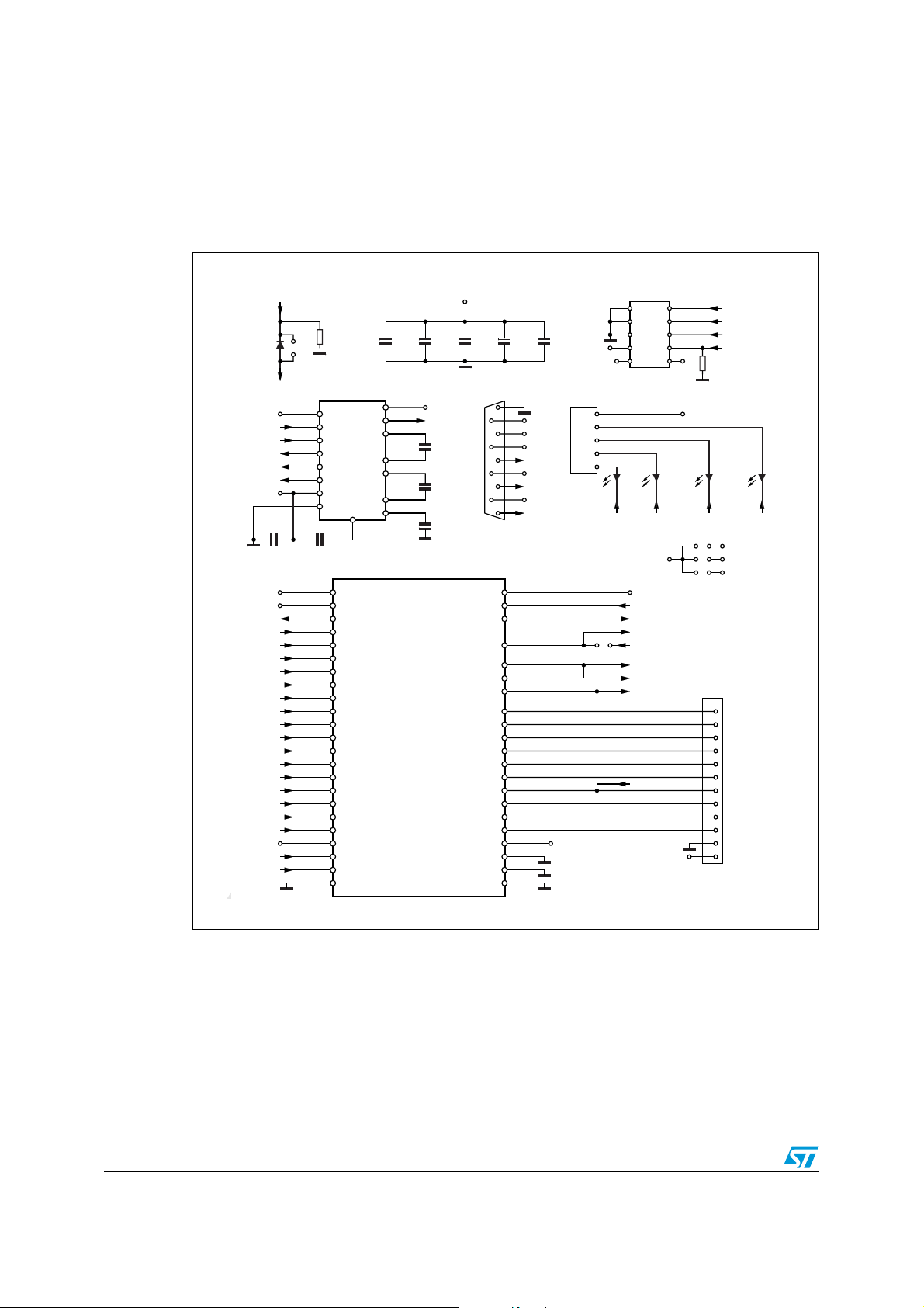
2.6 ST7 microcontroller and RS232 interface
To complete an application for the powerline communication a microprocessor must
manage the upper layer of the communication protocol and eventually process other signals
related to the application (signal from sensors, current measures, driving actuators, and so
on). A different type of microcontroller can be required depending on the specific
application.
The demonstration board has a ST72C334J2 or ST72C334J4 microprocessor. This
component is connected to the ST232 driver interface and to the ST7538Q.
The loaded firmware has the function to receive from the PC program interface (through the
standard RS232 serial port) some commands to manage the control register writing and
reading procedures as well as the transmitting and receiving functions of the modem. The
results of the executed command come back to the PC program interface and are displayed
on the monitor.
Figure 27. Microcontroller/RS232 interface
5V_led
ST72C334
PA7
PA7
PA6
PA6
PA5
PA5
PA4
PA4
1k
37
37
D9
36
36
35
35
34
34
D12
D10
1k 1k 1k
D11
RN1
CN5
PC INTERFACE
ST232
PE0/TD0
PE0/TD0
PE1/RDI
PE1/RDI
ANI0/PD0
ANI0/PD0
44
1
1
7
7
11
11
T1IN
12
12
R1OUT
10
T2IN
T1OUT
R1IN
T2OUT
T2OUT
14
14
13
13
7
7
2
3
1
T1OUT_A
R1IN_A
T2OUT_A
The ST7 microprocessor controls also the LED diodes D9, D10, D11, D12. The D9 (red) is
turned on during a transmission condition; the green LED D12 is turned on when the
receiving mode is activated. The D10 yellow diode is switched on when the Band-in-Use
signal is active. The D11 LED (red) is on when a Timeout event occurs. To save power
consumption the LEDs are turned off by removing jumper J9.
The ST7 firmware can be customized. Some of the I/O digital pins or analog input pins of
the microprocessor, that can be used to monitor some external signal or sensors and to
drive relays or other external devices, are available at the connector CN6.
The connector CN7 is used for ST7 memory in-situ programming. For a correct
programming procedure the ST7538Q has to be supplied, we suggest using an external 10
V supply from the connector CN2. The jumper J11 has to be opened.
30/46
Page 31

AN1714 Demonstration board for ST7538Q
If an emulator is linked to the board we recommend programming a 4 MHz clock in the
ST7538Q internal register.
For more accurate and complete information on the features, characteristics and issues
concerning ST microprocessors, please refer to the attached documentation or to the
reference documents or go to the site www.stmcu.com.
2.6.1 Modem / microcontroller interface
The interface signals between modem ST7538Q and the ST2C334 microcontroller can be
divided in three categories: the control signals, the communications signals and the auxiliary
signals.
The first group consists of the clock signal (MCLK/OSCIN) the reset signal (RSTO/RESET)
and the watchdog signal (WD/PD3).
The clock signal of the microcontroller is provided by the ST7538Q from the MCLK pin. The
default is 4Mhz but it is possible to increase this value (8 Mhz or 16 MHz) by programming
the ST7538Q control register.
The reset of the microcontroller is provided by the modem. The reset line is connected to the
manual reset (C
Programming mode procedures.
The watchdog signal has to be managed from the microcontroller (PD3 output port). If the
ST7538Q doesn't detect any activity on the WD pin, it generates a reset signal on the RSTO
pin. It is possible to disable this function through the modem control register.
, R15 and SW1) and to the reset pin of the CN7 connector for the In-Situ
22
The second group of signals consists of the links necessary for the modem/Micro Controller
Unit communication. These include the data signals RXD (from the modem to the MCU) and
TXD (from MCU to the modem), the transmitting/receiving status selection signal (RX/TX),
the internal ST7538Q register control access signal REG/DATA, and the recovery clock
signal CLRT.
The ISP (In Situ Programming mode) signals coming from the CN7 connector are also
linked to the communication wires and to the RESET. Remember to open the jumper J11
during the programming phase.
The simplest interfacing mode is the synchronous mode. In this case it is possible to use the
SPI interface of the MCU. The PC5/MOSI (Slave In Data) is connected to the RXD pin, the
PC4/MISO pin (Slave Out Data) is connected to the TXD pin and the PC6/SCKI (SPI serial
clock) pin is connected to the CLRT pin. The SPI Slave select (PC7/SS) is controlled by the
MCU itself through the PB0 I/O port.
The CLRT signal is connected to the PB1 I/O pin too.
It is also possible to implement an asynchronous interfacing mode, and for this reason the
pin RXD is also connected to the PC3/ICAP1_B pin (timer B input capture).
In this modality of communication the CLRT signal isn't considered and the recovered clock
has to be rebuilt internally by the MCU. If the ST7538Q control register has to be changed
from the default configuration, the first access has to be done at baud rate of 2400.
The idle state of the RXD output is the low state, so an asynchronous interface could be
necessary to invert externally this signal.
A diode (D
) and a pull down resistor R16 were inserted on the TXD connection line. With
13
these components it is possible to transmit a frame coming from an external device (for
example a BER tester). It is sufficient to configure the modem in a transmitting status and
31/46
Page 32

Demonstration board for ST7538Q AN1714
the MCU has to keep the PC4 pin low. The external signal can be applied at the diode
cathode.
Figure 28. ST7538Q / microcontroller interface
PC3/ICAP1_B
PC3/ICAP1_BPC3/ICAP1_B
PC4/MISO/ISPDATA
PC4/MISO/ISPDATA
PC4/MISO/ISPDATA
PC5/MOSI
PC5/MOSIPC5/MOSI
PC6/SCKI/ISPCLK
PC6/SCKI/ISPCLK
PC6/SCKI/ISPCLKPC6/SCKI/ISPCLK
MCO/PF0
MCO/PF0
MCO/PF0MCO/PF0
PF1/BEEP
PF1/BEEP
PF1/BEEPPF1/BEEP
ST72C334
ST72C334
OSCIN
OSCINOSCIN
RESET
RESETRESET
ANI4/PD3
ANI4/PD3
ANI4/PD3
ANI5/PD4
ANI5/PD4
ANI5/PD4
ANI6/PD5
ANI6/PD5
ANI6/PD5
PA3
PA331PA3
PF2
PF217PF2PF2
PB1
PB13PB1PB1
PB2
PB24PB2PB2
PB3
PB35PB3PB3
PB0
PB0PB0
PC7/SS
PC7/SSPC7/SS
ISPSEL
ISPSELISPSEL
42
42
39
39
C22
ISP RESET
26
26
27
27
27
28
28
29
29
29
10
10
10
11
11
11
12
12
12
31
31
15
15
15
16
16
16
17
17
3
3
4
4
5
5
2
2
30
30
38
38
ISP RESET
R17
R17
ISPDATA
ISPDATA
ISPCLOCK
ISPCLOCK
ISPSEL
ISPSEL
SW1
SW1
C22
D13
D13
J11
J11
11
11
MCLK
MCLK
12
12
R15
R15
R16
R16
3
3
5
5
8
8
14
14
43
43
4
4
1
1
42
42
9
9
15
15
7
7
36
36
RSTO
RSTO
RXD
RXD
TXD
TXD
CLRT
CLRT
WD
WD
REG/DATA
REG/DATA
RXTX
RXTX
CD/PD
CD/PD
PG
PG
BU
BU
ZCOUT
ZCOUT
TOUT
TOUT
REG_OK
REG_OK
ST7538
ST7538
Q
The third group of signals consists of a series of auxiliary signals coming from the ST7538Q
linked to some standard input of the microcontroller.
The CD/PD and BU signals give information about a carrier (or preamble detection)
condition and about the BU condition (according the EN50065-1).
If the zero-crossing comparator is used, the ZCOUT signal gives a digital signal
synchronized with the mains phase.
The PG, TOUT and REG_OK signals are monitor signals. The PG signal indicates the
correct supply level of the internal 5 V regulator of the ST7538Q (VDC). If the modem
regulator supplies the microcontroller or its reset is connected to the RSTO pin, it is
recommended to monitor this signal. In fact when the PG signal goes down during a
shutdown procedure, the microcontroller can try to correctly stop the running activities (for
example a memory writing) before the UVLO threshold is reached and the entire application
is reset, or before the regulator isn't able to correctly supply the micro. When a PG down is
detected, the transmission is disabled to avoid uncontrolled access to the mains. In any
case a correct shutdown procedure has to be completed to perform a correct reset of the
application.
The TOUT signal is active when a transmission procedure is aborted, either for a time out
event or for an overheat condition.
The REG_OK signal shows corruption of the internal modem register. Pay attention that the
REG_OK function doesn't check uncontrolled control register write procedure, due for
example, to a voltage spike on the REGDATA and RX/TX pins.
32/46
Page 33

AN1714 Demonstration board for ST7538Q
2.7 Bill of material
Table 3. Power supply sections
Item N Name Descriptions
1 1 CN1 Header 2
2 1 CN2 Header 2
3 1 C1 47 nF/250 V~ Y2, EVOX RIFA, PME271Y447M
4 2 C2 4.7 µF/400 V Rubycon YK, 400-YK-4R7-M-T8-10x16
C3 4.7 µF/400V Rubycon YK
5 2 C4 470 µF/16V Rubycon ZL, 16-ZL-470-M-T8-10x12.5
C5 470 µF/16 V Rubycon ZL
6 1 C6 22 µF/50 V
7 1 C7 2.2 nF/250 V~ Y1 Ceramite, 440LD22
8 1 C8 1 µF
C9
91C10 1 µF
10 1 C34 100 nF/100 V
C35
11 1 D1 Rectifier 380 V/1.5 A, B380C1500M
12 1 D2 STPS160A SMA
13 1 D3 BZW06-171
14 1 D4 STTA106
15 1 D5 LED green
16 2 D6 1N4148
D7 1N4148
17 1 F1 TR5-F 250 V 500 mA, Wickmann, 370.0500.041
18 3 J1 Jumper closed
J4 Jumper closed
J5 Jumper closed
19 1 L1 2x10 mH 0.3 A, Radi
L1 2x10 mH 0.25 A, TDK UF1717V-103YR25-02
20 1 L2 220 µH series BC, Siemens Matsushita B781.8-S1224-J
21 1 L3 10 µH series BC, Siemens Matsushita B781.8-S1103-K
22 1 L5 1mH series LBC, Siemens Matsushita B82144-A2105-J
Ω 42 V15
23 1 R1 15
24 1 R2 2.2 k
25 1 R3 22
Ω, 3 W metal film
Ω SMD
Ω
33/46
Page 34

Demonstration board for ST7538Q AN1714
Table 3. Power supply sections (continued)
Item N Name Descriptions
R4
26 1 R_L6 10
Ω
27 1 R5 3320 Ω
28 1 R7 910 Ω
29 1 TR1 0.7mH, Radiohm 69E16H.1B
TR1 0.7mH, TDK SRW16ES-ExxH004
30 1 U1 L6590
Table 4. Powerline modem section
Item N Name Descriptions
1 1 CN3 Header 2
2 1 CN4 Header 7
3 1 C11 33 nF 220 V/X2
4 1 C13 220 nF MKT
5 2 C14 10 µF TANT SMD, AVX, TPSW106*016#0600
C30 10 µF TANT SMD
6 1 C38 10 µF TANT SMD, VISHAY, 293D106X_035D2_
7 4 C15 100 nF SMD
C16 100 nF SMD
C20 100 nF SMD
(1)
, EVOX RIFA, PHE840EB5330MR17
(1)
, EPCOS B32529-C1224-K
C21 100 nF SMD
8 1 C17 6.8 nF, ARCOTRONIX, R82EC1680AA5J
9 1 C18 47 pF SMD
10 1 C19 18 pF SMD
11 1 C33 10 nF CERAMIC
12 1 C36 4.7 nF MKP 5%
13 1 C37 100 pF SMD
14 1 C_R9 100 nF MKT
D8
D14
15 2 D15 P6KE6V8A
D16 P6KE6V8A
16 1 D17 SM6T6V8A
17 3 J2 Jumper closed
J3 Jumper closed
34/46
(1)
, EVOX RIFA, PFR5-472J63L4
(1)
, EPCOS, B32520-C3104-K
Page 35

AN1714 Demonstration board for ST7538Q
Table 4. Powerline modem section (continued)
Item N Name Descriptions
J7 Jumper closed
18 1 J6 CON3
(1)
19 1 L_C12 10 µH LBC Inductor
20 1 L4 22 µH 10% series LBC
21 1 L7 330 µH 5% series BC
22 1 L8 10 µH SMD
23 1 R8 4.7 M
24 1 R10 5 Ω, 1/4 Watt
25 1 R11 750
26 1 R12 50 kΩ TRIM
, Siemens Matsushita B82144-A2103-K
(1)
, Siemens Matsushita B82144-A2223-K
(1)
, Siemens Matsushita B781.8-S1334-J
Ω
Ω
27 1 R13 5 k
28 1 R14 1 k
Ω TRIM
Ω
29 1 T1 VACuumschmelze T60403-F4096-X046, 1.7 mH, 1:1 transformer
T1 TDK TRTT10U-E015A012, 2 mH, 1:1 transformer
T1 SECRE T15253, 1.3 mH, 1:1 transformer
T1 ETAL P2824, 1.2 mH, 1:1 transformer
T1 RADIOHM 63V192100, 2 mH, 2:1 transformer
30 1 U2 ST7538Q (TQFP44 CTI7010 – 044)
31 1 X1 16 M, quartz crystal, Q 16.0-SS3-30-30/30-FU-T1
1. Values for 132.5KHz communication channel
Table 5. ST7/RS232 section
Item N Name Descriptions
1 1 CN5 RS232 female 9 Pin
2 1 CN6 CON12
3 1 CN7 ISP interface
4 9 C23 100 nF SMD
C24 100 nF SMD
C25 100 nF SMD
C26 100 nF SMD
C27 100 nF SMD
C28 100 nF SMD
C29 100 nF SMD
C31 100 nF SMD
C32 100 nF SMD
35/46
Page 36
Demonstration board for ST7538Q AN1714
Table 5. ST7/RS232 section (continued)
Item N Name Descriptions
5 1 C22 22 nF SMD
61D12 LED green
7 2 D9 LED red
D11 LED red
81D10 LED yellow
9 1 D13 1N4148 SMD
10 5 JL1 Jumper open
J8 Jumper closed
J9 Jumper closed
J10 Jumper closed
J11 Jumper closed
11 1 RN1 R_STRIP 1 k
Ω 4resis
12 1 R15 4.7 k
13 1 R16 47 k
14 1 R17 10 k
15 1 SW1 SW pushbutton
16 1 U3 ST232B
17 1 U4 ST72C334J4 TQFP44 SMT
Ω SMD
Ω SMD
Ω
36/46
Page 37
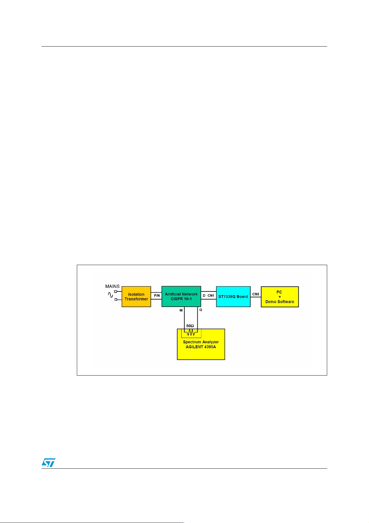
AN1714 Demonstration board characterization
3 Demonstration board characterization
This chapter includes a series of tests and measurements to characterize the demonstration
board. The characterization concerns the most critical aspects required by European
standards which are:
1. Electro-conducted disturbances
2. Immunity to narrowband conducted noise
3. Output impedance measurement
The results of these measures show a good match and a very close value to the measures
done according to the EN50065-1, EN50065-2-1 and EN50065-7 setup and procedures.
3.1 Conducted disturbance
The EN50065-1 standard describes the test setup and procedures for these kinds of tests.
The measures have been done with 220 V~ and 110 V~ mains voltages. The test pattern
consists of a continuous transmission of a fixed tone (symbol "0") or a repetition of random
bytes.
The output signal has a peak value of 118dBuV (output CISPR-16 measure of the not
modulated signal) that means a 1.6V
The spectrum analyzer performs a peak measure instead of a quasi-peak measure. For
continuous sinusoidal signals the two types of measures give the same result.
of signal on the mains.
rms
Figure 29. Conducted disturbance setup
As shown by the spectrum plots the point that is usually the closest to the mask is the 2
harmonic. The borderline condition is obtained with the 110 V~ mains supply and with the
110 kHz channel.
In the 110 kHz channel case the output board filter centered at the 132.5 kHz channel
produces lower attenuation of the harmonic.
The other critical condition is with the 110 V~ supply. In this case the switching regulator
gives a lower supply voltage. The effect is to compress the top of the output sinusoidal
nd
37/46
Page 38
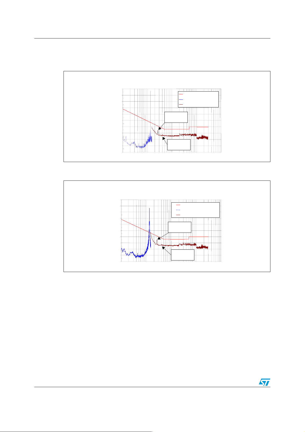
Demonstration board characterization AN1714
signal producing higher odd harmonics. The difference is some hundreds of microvolts but
considering the strong constraints of the norm they are relevant.
Figure 30. Output signal spectrum, channel 132.5 kHz, mains 220 V~, fixed tone
Ch 132.5 kHz, baud 2400, dev 0,5
dBuV
120.0
110.0
100.0
90.0
80.0
70.0
60.0
50.0
40.0
30.0
20.0
Continuos Transmission - Fix Tone "0"
EN50065-1
10kHz -> 150kH z (Bw = 100Hz)
150kHz -> 30MHz (Bw=10kHz)
nd
2
Harmonic
54.3dBµV
rd
3
Harmonic
47.9dBµV
10000 100000 1000000 10000000 100000000
Figure 31. Output signal spectrum, channel 132.5 kHz, mains 220 V~, random
sequence
dBuV
120.0
110.0
100.0
90.0
80.0
70.0
60.0
50.0
40.0
30.0
20.0
10000 1000 00 1000000 10000000 100000000
Ch 132.5 kHz, baud 2400, dev 0,5
Continuos Transmission - Random Sequences
EN50065-1
10kHz -> 150kHz (Bw = 100Hz)
150kHz -> 30MHz (Bw =10kHz)
nd
2
Harmonic
54.3dBµV
rd
3
Harmonic
47.8dBµV
38/46
Page 39

AN1714 Demonstration board characterization
Figure 32. Output signal spectrum, channel 132.5 kHz, mains 110 V~, random
sequence
dBuV
Ch 132.5 kHz, baud 2400, dev 0,5 - mains 110V~
Continuos Transmission - Random Sequences
120.0
110.0
100.0
90.0
80.0
70.0
60.0
50.0
40.0
30.0
20.0
10000 100000 1000000 10000000 100000000
EN50065-1
10kHz -> 150kHz (Bw = 100Hz)
150kHz -> 30MHz (Bw =10kHz)
nd
2
Harmonic
54.0dBµV
rd
3
Harmonic
47.2dBµV
Figure 33. Output signal spectrum, channel 110 kHz, mains 220 V~, random
sequence
Ch 110 kHz, baud 2400, dev 0,5
dBuV
120.0
110.0
100.0
Continuos Transmission - Random Sequence s
EN50065-1
10kHz -> 150kHz (Bw = 100Hz)
90.0
80.0
70.0
60.0
50.0
40.0
30.0
20.0
10000 10000 0 1000000 10000000 100000000
150kHz -> 30MHz (Bw=10kHz)
nd
2
Harmonic
54.0dBµV
rd
3
Harmonic
47.2dBµV
3.2 Narrowband conducted interference
The setup of the narrowband conducted interferences test consists of a first transmitting
demonstration board controlled by a BER (Bit Error Rate) tester that generates a random bit
stream. The second board demodulates the received signal that is evaluated by the linked
BER tester.
The noise is produced by a waveform generator and injected into the artificial network by a
coupling circuit connected to a low distortion power amplifier (EN50065-2-1, 7.2.3).
Two types of signal noises have been used for the test: a pure sinusoidal signal and an
amplitude-modulated signal, (modulating signal 1 kHz, modulation deep 80%).
The amplitude of the noise signal is decreased until the BER measured is lower than 10
(one error every 1000 transmitted bits).
The noise measure is done disconnecting the signal source and the coupling circuits from
the artificial network.
-3
39/46
Page 40

Demonstration board characterization AN1714
Figure 34. Narrowband conducted interferences setup
The following are different measurements with a transmitted signal of 79dBuV measured at
the CISPR-16 output (minus 6dB versus mains). A measure of the 110 kHz channel (signal
level 85dBuV) is also present even if the receiving filter of the board is tuned on the 132.5
kHz channel.
The power amplifier used represents a limit for the measure with respect to the maximum
noise voltage level. In fact for the noise tones far from the channel frequency, the BER
obtained is zero and the power amplifier isn't able to produce a higher sinusoidal noise.
Figure 35. Signal/noise ratio for the 132.5 kHz channel, signal level 85 dBuV
S/N
15
10
5
0
-5
-10
-15
-20
-25
-30
-35
-40
-45
-50
80 90 100 110 120 130 140 150 160 170 180 190 200
Ch 132.5KHz, BAUD 2400, DEV 0. 5
S = 85 dBuV, BER < 10e-3 - mains 220V~
Fix Tone
AM 1kHz - 80%
FREQ[KHz]
40/46
Page 41

AN1714 Demonstration board characterization
Figure 36. Signal/noise ratio for the 132.5 kHz channel, signal level 85 dBuV, mains
110 V~
S/N
Ch 132.5KHz, BAUD 2400, DEV 0.5
S = 85 dBuV, BER < 10e-3 - mains 110V~
15
10
5
0
Fix Tone
AM 1kHz - 80%
-5
-10
-15
-20
-25
-30
-35
-40
-45
-50
80 90 100 110 120 130 140 150 160 170 180 190 200
FREQ[KHz]
Figure 37. Signal/noise ratio for the 110 kHz channel, signal level 91 dBuV
S/N
20
15
10
5
0
-5
-10
-15
-20
-25
-30
-35
-40
-45
80 90 100 110 120 130 140 150 160 170 180
Ch 110KHz, BAUD 2400, DEV 0.5
S = 91 dBuV, BER < 10e-3 - mains 220V~
Fix Tone
AM 1kHz - 80%
FREQ[KHz]
3.3 Output impedance
The last characterization report concerns the output impedances of the application.
In order to not degrade the communication network it is mandatory to guarantee a minimum
value of the output impedance of each component of the system, both in the receiving and
transmitting condition. In this last case impedance constraints concern only the frequency
ranges of the other communication bands.
41/46
Page 42

Demonstration board characterization AN1714
Figure 38. Output board impedance measurement setup
The reference standard is the EN50065-7. To simplify the measurement, the supply of the
board is obtained by a low 10 V external power supply and the impedance meter has been
connected directly to the mains connector.
Figure 39 and 40 show the normative mask for the home appliance band (95 kHz - 148.5
kHz).
Figure 39. Output demonstration board impedances (CN1) in receiving condition
ohm
1000
100
10
1
10 30 50 70 90 110 130 150
Receiving Condition
EN50065-7
Z_RX
KHz
Figure 40. Output demonstration board impedances (CN1) in transmitting condition
ohm
1000
100
10
Transmitting Condition
EN50065-7
Z_TX
1
10 30 50 70 90 110 130 150
42/46
KHz
Page 43

AN1714 Design ideas for auxiliary blocks
4 Design ideas for auxiliary blocks
4.1 Zero-crossing detector
It is possible to synchronize the beginning of the transmission with the mains voltage (phase
0). To implement this function the zero-crossing comparator has to be used and a reduced
reproduction of the mains frequency (with the same phase) has to be present on the ZCin
pin (#16). The maximum voltage of this pin is ±5 V.
In case of a nonisolated application the circuit consists of a simple resistor divider. For an
isolated system a possible solution could be a mains transformer. This solution is more
expensive and is suggested only if such a mains transformer is also used in the application
for another purpose.
It is possible to implement another isolated solution using for example an optocoupler
component also.
In both cases a bidirectional transil has to protect the pin from the burst and surge and a
capacitor have to be added to filter high frequency noise.
Figure 41. Zero-crossing coupling circuit, nonisolated solutions
Q
ST7538
ST7538
ZCout
ZCout
15
Tx Sync
Tx Sync
ZCin
ZCin
15
16
16
25
25
10 MΩ
10 MΩ
100 KΩ
100 KΩ
Figure 42. Zero-crossing coupling circuit, isolated solutions
ST7538
ST7538
Q
ZCout
ZCout
15
15
100 KΩ
Tx Sync
Tx Sync
ZCin
ZCin
16
16
25
25
100 KΩ
100 KΩ
100 KΩ
1
1
50
50
P
P
MAINS
MAINS
N
N
MAINS
MAINS
43/46
Page 44

Documentation AN1714
Appendix A Documentation
4.2 ST7538Q
● ST7538Q datasheet
● Demonstration board user manual
● EHS Booklet
4.3 L6590 integrated power supply
● L6590 datasheet
● Application note AN1261
● Application note AN1262
● Application note AN1523
4.4 ST7 microprocessor
ST72 series datasheet
4.5 Surge and burst protections
● Protection guide
● Application note AN317
● Application note AN576
44/46
Page 45

AN1714 References
5 References
1. SGS-THOMSON - Power Line Modem & Applications data book - September 1994
2. CENELEC, European Committee for Electrotechnical Standardization - EN 50065-1,
Signaling on low-voltage electrical installations in the frequency range 3 kHz to
148,5 kHz. Part 1: General requirements, frequency bands and electromagnetic
disturbances - July 2001
3. CENELEC, European Committee for Electrotechnical Standardization - EN 50065-4-2,
Signaling on low-voltage electrical installations in the frequency range 3 kHz to 148,5
Khz. Part 4-2: Low voltage decoupling filters- Safety requirements - August 2001
4. CENELEC, European Committee for Electrotechnical Standardization - EN 50065-7,
Signaling on low-voltage electrical installations in the frequency range 3 kHz to
148,5 Khz. Part 7: Equipment impedance - November 2001
5. CENELEC, European Committee for Electrotechnical Standardization - prEN 50065-21, Signaling on low-voltage electrical installations in the frequency range 3 kHz to
148,5 kHz. Part 2-1: Immunity requirements for mains Communications Equipment and
systems operating in the range of frequencies 95 kHz to 148,5 kHz and intended for
use in Residential, Commercial and Light Industrial Environments - 1999
6. IEC, International Electrotechnical Commission, International Special Committee On
Radio Interferences - CISPR 16-1, Specification for radio disturbance and immunity
measuring apparatus and methods. Part 1: Radio disturbance and immunity measuring
apparatus - first edition, August 1993
7. EHSA, European Home System Association - EHS specifications, version 1.3a -
May 2001.
6 Revision history
Table 6. Document revision history
Date Revision Changes
21-Jun-2006 3 Minor text changes
27-Feb-2008 4
–
Section 1.2 added
Section 2.4 modified
–
– ST7538 replaced by ST7538Q
– Content reworked to improve readability, no content changes
45/46
Page 46

AN1714
Please Read Carefully:
Information in this document is provided solely in connection with ST products. STMicroelectronics NV and its subsidiaries (“ST”) reserve the
right to make changes, corrections, modifications or improvements, to this document, and the products and services described herein at any
time, without notice.
All ST products are sold pursuant to ST’s terms and conditions of sale.
Purchasers are solely responsible for the choice, selection and use of the ST products and services described herein, and ST assumes no
liability whatsoever relating to the choice, selection or use of the ST products and services described herein.
No license, express or implied, by estoppel or otherwise, to any intellectual property rights is granted under this document. If any part of this
document refers to any third party products or services it shall not be deemed a license grant by ST for the use of such third party products
or services, or any intellectual property contained therein or considered as a warranty covering the use in any manner whatsoever of such
third party products or services or any intellectual property contained therein.
UNLESS OTHERWISE SET FORTH IN ST’S TERMS AND CONDITIONS OF SALE ST DISCLAIMS ANY EXPRESS OR IMPLIED
WARRANTY WITH RESPECT TO THE USE AND/OR SALE OF ST PRODUCTS INCLUDING WITHOUT LIMITATION IMPLIED
WARRANTIES OF MERCHANTABILITY, FITNESS FOR A PARTICULAR PURPOSE (AND THEIR EQUIVALENTS UNDER THE LAWS
OF ANY JURISDICTION), OR INFRINGEMENT OF ANY PATENT, COPYRIGHT OR OTHER INTELLECTUAL PROPERTY RIGHT.
UNLESS EXPRESSLY APPROVED IN WRITING BY AN AUTHORIZED ST REPRESENTATIVE, ST PRODUCTS ARE NOT
RECOMMENDED, AUTHORIZED OR WARRANTED FOR USE IN MILITARY, AIR CRAFT, SPACE, LIFE SAVING, OR LIFE SUSTAINING
APPLICATIONS, NOR IN PRODUCTS OR SYSTEMS WHERE FAILURE OR MALFUNCTION MAY RESULT IN PERSONAL INJURY,
DEATH, OR SEVERE PROPERTY OR ENVIRONMENTAL DAMAGE. ST PRODUCTS WHICH ARE NOT SPECIFIED AS "AUTOMOTIVE
GRADE" MAY ONLY BE USED IN AUTOMOTIVE APPLICATIONS AT USER’S OWN RISK.
Resale of ST products with provisions different from the statements and/or technical features set forth in this document shall immediately void
any warranty granted by ST for the ST product or service described herein and shall not create or extend in any manner whatsoever, any
liability of ST.
ST and the ST logo are trademarks or registered trademarks of ST in various countries.
Information in this document supersedes and replaces all information previously supplied.
The ST logo is a registered trademark of STMicroelectronics. All other names are the property of their respective owners.
© 2008 STMicroelectronics - All rights reserved
STMicroelectronics group of companies
Australia - Belgium - Brazil - Canada - China - Czech Republic - Finland - France - Germany - Hong Kong - India - Israel - Italy - Japan -
Malaysia - Malta - Morocco - Singapore - Spain - Sweden - Switzerland - United Kingdom - United States of America
www.st.com
46/46
 Loading...