

Page 1

AN1709
APPLICATION NOTE
EMC DESIGN GUIDE
FOR ST MICROCONTROLLERS
by Cyril Troise - Microcontroller Division Applications
INTRODUCTION
The continuing demand for more performance, complexity and cost reduction require the semiconductor industry to develop Microcontrollers with both high density design technology and
higher clock frequencies. This has intrinsically increased the noise emission and noise sensitivity. Applic ation dev elope rs therefor e, must no w app ly EMC “h ardening” te chniqu es in the
design of firmware, PCB layout and at system level. This note aims to explain ST Microcontroller EMC features and compliance standards to help application designers reach the optimum level of EMC performance.
1.0
AN1709/1003 1/38
1
Page 2

Table of Contents
INTRODUCTION . . . . . . . . . . . . . . . . . . . . . . . . . . . . . . . . . . . . . . . . . . . . . . . . . . . . . . . 1
1 EMC DEFINITIONS . . . . . . . . . . . . . . . . . . . . . . . . . . . . . . . . . . . . . . . . . . . . . . . . . . . . 4
1.1 EMC . . . . . . . . . . . . . . . . . . . . . . . . . . . . . . . . . . . . . . . . . . . . . . . . . . . . . . . . . . . 4
1.2 EMS . . . . . . . . . . . . . . . . . . . . . . . . . . . . . . . . . . . . . . . . . . . . . . . . . . . . . . . . . . . 4
1.3 EMI . . . . . . . . . . . . . . . . . . . . . . . . . . . . . . . . . . . . . . . . . . . . . . . . . . . . . . . . . . . . 4
2 EMC CHARACTERIZATION OF ST MICROCONTROLLERS . . . . . . . . . . . . . . . . . . 5
2.1 ELECTROMAGNETIC SU SCEPTIBILITY (EM S) . . . . . . . . . . . . . . . . . . . . . . . . 5
2.1.1 Functional EMS test . . . . . . . . . . . . . . . . . . . . . . . . . . . . . . . . . . . . . . . . . . . . . . . . . . 5
2.1.1.1 Functional ElectroStatic Discharge Test (F_ESD Test) . . . . . . . . . 5
2.1.1.2 Fast Transient Burst (FTB) . . . . . . . . . . . . . . . . . . . . . . . . . . . . . . . 7
2.1.1.3 ST Severity Level & Behavior Class . . . . . . . . . . . . . . . . . . . . . . . 8
2.1.2 Latch-Up (LU) . . . . . . . . . . . . . . . . . . . . . . . . . . . . . . . . . . . . . . . . . . . . . . . . . . . . . 10
2.1.2.1 Static Latch-Up (LU) test: . . . . . . . . . . . . . . . . . . . . . . . . . . . . . . . 10
2.1.2.2 Dynamic Latch-Up (DLU) test: . . . . . . . . . . . . . . . . . . . . . . . . . . . 10
2.1.3 Absolute Electrical Sensitivity . . . . . . . . . . . . . . . . . . . . . . . . . . . . . . . . . . . . . . . . . 11
2.1.3.1 Human Body Model Test Sequence . . . . . . . . . . . . . . . . . . . . . . 12
2.1.3.2 Machine Model Test Sequence . . . . . . . . . . . . . . . . . . . . . . . . . . 12
2.2 ELECTROMAGNETIC INTERFERENCE (EMI) . . . . . . . . . . . . . . . . . . . . . . . . . 13
2.2.1 EMI radiated test . . . . . . . . . . . . . . . . . . . . . . . . . . . . . . . . . . . . . . . . . . . . . . . . . . . 13
2.2.2 EMI level classification . . . . . . . . . . . . . . . . . . . . . . . . . . . . . . . . . . . . . . . . . . . . . . . 16
3 ST MCU DESIGN STR ATEGY & EMC SPECIFIC FEATURE . . . . . . . . . . . . . . . . . . 17
3.1 SUSCEPTIBILITY . . . . . . . . . . . . . . . . . . . . . . . . . . . . . . . . . . . . . . . . . . . . . . . . 17
3.1.1 Low Voltage Detector (LVD) . . . . . . . . . . . . . . . . . . . . . . . . . . . . . . . . . . . . . . . . . . 17
3.1.2 Auxiliary Voltage Detector (AVD) . . . . . . . . . . . . . . . . . . . . . . . . . . . . . . . . . . . . . . . 19
3.1.3 I/O Features & properties . . . . . . . . . . . . . . . . . . . . . . . . . . . . . . . . . . . . . . . . . . . . . 21
3.1.3.1 Electrostatic Discharge and Latch-up . . . . . . . . . . . . . . . . . . . . . 21
3.1.3.2 Protective Interface . . . . . . . . . . . . . . . . . . . . . . . . . . . . . . . . . . . 22
3.1.3.3 Internal Circuitry: Digital I/O pin . . . . . . . . . . . . . . . . . . . . . . . . . . 23
3.1.3.4 Internal Circuitry: Analog Input pin . . . . . . . . . . . . . . . . . . . . . . . . 25
3.1.4 Multiple VDD & VSS. . . . . . . . . . . . . . . . . . . . . . . . . . . . . . . . . . . . . . . . . . . . . . . . . 26
3.2 EMISSION . . . . . . . . . . . . . . . . . . . . . . . . . . . . . . . . . . . . . . . . . . . . . . . . . . . . . 27
3.2.1 Internal PLL . . . . . . . . . . . . . . . . . . . . . . . . . . . . . . . . . . . . . . . . . . . . . . . . . . . . . . . 27
3.2.2 Global low power approach . . . . . . . . . . . . . . . . . . . . . . . . . . . . . . . . . . . . . . . . . . . 27
3.2.2.1 Low powered oscillator . . . . . . . . . . . . . . . . . . . . . . . . . . . . . . . . . 27
38
3.2.2.2 Internal Voltage Regulators (for MCUs with low power core). . . . 29
2/38
1
Page 3

Table of Contents
3.2.3 Output I/O Current limitation & edge timing control . . . . . . . . . . . . . . . . . . . . . . . . . 29
4 EMC GUIDELINES FOR MCU BASED APPLICATIO NS . . . . . . . . . . . . . . . . . . . . . 30
4.1 HARDWARE . . . . . . . . . . . . . . . . . . . . . . . . . . . . . . . . . . . . . . . . . . . . . . . . . . . . 30
4.2 HANDLING PRECAUTIONS FOR ESD PROTECTION. . . . . . . . . . . . . . . . . . . 34
4.3 FIRMWARE . . . . . . . . . . . . . . . . . . . . . . . . . . . . . . . . . . . . . . . . . . . . . . . . . . . . 36
4.4 WEB LINKS TO EMC RELATE D ORGANIS AT IONS . . . . . . . . . . . . . . . . . . . . 36
5 CONCLUSION . . . . . . . . . . . . . . . . . . . . . . . . . . . . . . . . . . . . . . . . . . . . . . . . . . . . . . 37
3/38
Page 4

EMC DESIGN GUIDE FOR ST MICROCONTROLLERS
1 EMC DEFIN ITI ONS
1.1 EMC
ElectroMagnetic Comp atibility (EMC) is the cap ability of a system to work prop erly, undisturbed by the electromagnetic phenomena present in its normal environment, and not to
create electrical disturbances that would interfere with other equipment.
1.2 EMS
The ElectroMagnetic Susceptibility (EMS) l evel of a device is the resistance to electrical disturbances and conducted electrical noise. ElectroStat ic Discharge (ESD ) and Fast Transient
Burst (FTB) tests determine the reliability level of a device operating in an undesirable electromagnetic environment.
1.3 EMI
The ElectroMagnetic Interference (EMI) is the level of conducted or radiated electrical noise
sourced by the equipment. Conducted emission propagates along a cable or any interconnection line. Radiated emission propagates through free space.
4/38
2
Page 5
EMC DESIGN GUIDE FOR ST MICROCONTROLLERS
2 EMC CHARA CTERIZATION OF ST MICROC ONTROLLERS
2.1 ELECTROMAGNETIC SUSCEPTIBILITY (EMS)
Two different type of tests are performed:
■ Tests with device power-supplied (Functional EMS tests & Latch-up): The device behaviour
is monitored during the stress.
■ One test with device not powered supplied (Absolute Electrical Sensitivity): The device
functionality and integrity is checked on tester after stress.
2.1.1 Functional EMS test
Functional Tests are performed to measure the robustnes s of ST Microcontrollers running in
an application. Based on a simple program (toggling 2 LEDs through I/O ports), the product is
stressed by 2 different EMC events until a run-away condition (failure) occurs.
2.1.1.1 Functional ElectroStatic Discharge Test (F_ESD Test)
This test is performed on any new microcontroller devices.Each pin is tested individually with
a single positive or negative electrical discharge.This allows failures investigations inside the
chip and further application recommendations to protect the concerned Microcontroller sensitive pins against ESD.
High static voltage has both natural and man m ade origins. Some specific equipment can reproduce t his phenom e non i n orde r to te st t he devi ce un der r eal con di tions. Eq ui pmen t, test
sequence and standards are described here below.
ST Microcontroller F_ESD qualification test uses standards given in Table 1 as reference.
Table 1. ESD standards
EUROPEAN NORM INTERNATIONAL NORM DESCRIPTION
EN 61000-4-2 IEC 1000-4-2 Conducted ESD test
AEC-Q100-REUE is the Automotive controlling document.
F_ESD tests uses a signal source and a power amplifi er to generate a hi gh l evel fi eld into The
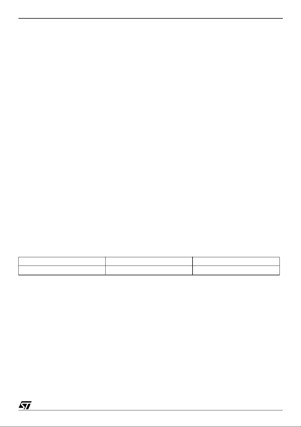
Microcontroller. The insulator is using a conical tip. This tip is placed on the Device or Equipment Under Test (DUT or EUT) and an electrostatic discharge is applied (see Figure 1.).
5/38
Page 6
EMC DESIGN GUIDE FOR ST MICROCONTROLLERS
Figure 1. ESD test equipment
ground plane
ESD generator
insulation
EUT
mains
connections
The equipment used to perform F_ESD test is a Generator NSG 435 (SCHAFFNER) compliant with the norm IEC 1000-4-2. The discharges are directly applied on ea ch pin of the
MCU.
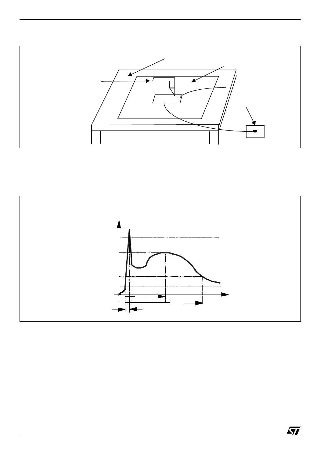
Figure 2. Typical ESD Current Waveform in Contact -mode discharge
(EN 61000-4-2)
Current
100%
90%
I(30ns)
I(60ns)
6/38
10%
30ns
tr=0.7 to 1.0 ns
60ns
time
Page 7
EMC DESIGN GUIDE FOR ST MICROCONTROLLERS
Figure 3. Simplified diagram of the ESD generator
Discharge
tip
Discharge return
connection
ESD
generator
Rch
Rd
HV relay
Cs = 150 pF
(Rch = 50MΩ; Rd = 330Ω)
2.1.1.2 Fast Transient Burst (FTB)
More complex than functional ESD, this test which su bmits the dev ice to a large quant ity of
emitted disturbances in a short time, is useful for detecting infrequent and unrecoverable
(Class B or C) Microcontroller states. FTB disturbances (see Figure 4.) are applied to the Mi-
crocontroller power lines through a capacitive coupling network.
ST Microcontroller FTB test correlates with the standards given in Table 2
Table 2. FTB standards
EUROPEAN NORM INTERNATIONAL NORM DESCRIPTION
EN61000-4-4 IEC 1000-4-4 Fast Transient Burst
Figure 4. FTB Waveform Diagram
Voltage
Burst
Time
Burst Length
15ms
Repetition Frequency: 5kHz; Bursts will
be repeated for at least 1 minute.
Burst Period
300ms
Voltage
Pulse
Bur
s
t
Time Time
Rising and Durat ion time (±3 0%) are referred to a 50Ω load
Volt age
0.9Vpk
0.1Vpk
5ns
Vpk
0.5Vpk
50ns
The spike frequency is 5 kHz. The generator produces bursts of spikes that last 15 ms every
300 ms (75 spikes).
The fast transients are coupled to the device DUT with capacitors C
(See Figure 5.).
C
7/38
Page 8
EMC DESIGN GUIDE FOR ST MICROCONTROLLERS
Figure 5. Coupling Network
NSG 2025
+V
POWER
SUPPLY
GND
DD
L
Cc
Cc
+V
DD
TO THE DEVICE
UNDER TEST
GND
Measurements are performed on a ground plane. The generator is connected to ground plane
by a short wire. The supply wires are 10 cm from the ground pl ane. The DU T is on the insulator 10 cm from the ground plane. The FTB voltage level is increased until the device failure.
Severity Levels and Class help application designers to determine which ST microcontrollers
are suitable for their target application, based on the susceptibility level (Severity level) and
type of behavior (Class) indicated in the datasheet.
2.1.1.3 ST Severity Level & Behavior Class
The 1000-4-2 and 1000-4-4 standards do not refer specifically to semiconductor components
such as microcontrollers. Us ually electromagne tic stress is app lied on other pa rts of the
system such a s connec tors, m ains , supp lies... Th e en ergy le vel o f th e F_E SD and FTB test
decreases before reaching the microcontroller, governed by the laws of physics. A large
amount of statistical data collected by ST on the behaviour of MCUs in various application environments has been used to develop a correlation chart between ST F_ESD or FTB test
voltage and 1000-4-2/1000-4-4 severity levels (See Table 3).
Table 3. ST ESD Severity levels
Severity Level
120.50-0.5
2410.5-1
3621-1.5
484>1.5
ESD (1000-4-2)
Equipment standard
(kV)
FTB (1000-4-4)
Equipment standard
(kV)
ST Testing Voltage
ST internal EMC test
(kV)
In addition to th is severity le vel, MCU beh aviour under ESD stress can be grouped into different Behaviour Classes (See Table 4) according to EN 50082-2 norm:
8/38
Page 9
EMC DESIGN GUIDE FOR ST MICROCONTROLLERS
Table 4. ST Behavior Classes
Class A Class B Class C Class D
Needs an external user
action to recover normal
functionality
Normal functionality
cannot be recovered
No failure detected
Failure detected but self
recovery after disturbance
Any ST Microcontroller under the “acc eptance limits” is rejected as a fail. The “target level” is
the level used by ST to define good EMS performance.
Class B could be caused by:
– a parasitic reset correctly managed by the firmware (preferable case).
– deprogramming of a peripheral register or memory recovered by the application.
– a blocked status, recovered by a Watchdog or other firmware implementation.
Class C could be caused by:
– deprogramming of a peripheral register or memory not recovered by the application.
– a blocked application status requiring an external user action.
Table 5 shows ST target and acceptance limits.
Table 5. F_ESD / FTB target level & acceptance limit
Acceptance limit Target Level
F_ESD 0.5kV >1kV
FTB 0.5kV >1.5kV
Between “Acce ptance limit” and “T arget Level”, the dev ice is relatively suscep tible to noise.
Special care during system design should be taken to avoid susceptibility issues.
Table 6 shows how F_ESD / FTB test results are presented in ST datasheets.
Table 6. Example of F_ESD / FTB test results
Symbol Ratings Conditions Severity/Criteria
V
F_ESD
V
FTB
Voltage limits to be applied on any I/O
pin to induce a functional disturbance
Fast transient voltage burst limits to
be applied through 100pF on VSS and
VDD pins to induce a functional disturbance
T
=+25°C 2/A, 3/B
A
T
=+25°C 3/B
A
9/38
Page 10
EMC DESIGN GUIDE FOR ST MICROCONTROLLERS
2.1.2 Latch-Up (LU)
2.1.2.1 Static Latch-Up (LU) test:
The Latch-up is a phenomenon which is defined by a high current consumption resulting from
an overstress that triggers a parasitic thyristor structure and need a disconnection of the
power supply to recover the initial state.
NOTES
1 The overstress can be a voltage or current surge, an excessive rate of change of current or
voltage , or any other abno rmal conditi on th at caus es the paras itic th yrist or str ucture t o become self-sustaining.
2 Latch-up will not damage the device if the current through the low-impedance path is sufficiently limited in magnitude or duration.
This test conforms to the EIA/JESD 78 IC latch-up standard.
True LU is self-sustaining and once triggered, the h igh current c ondition w ill remain unt il the
power supply voltage is removed from the device. A temporary LU condition is considered to
have been induced if the high current condition stops when only the trigger voltage is removed.
Two complementary static tests are required on 10 parts to assess the latch-up performance:
■ Power supply overvoltage (applied to each power supply pin) simulates a user induced
situation where a transient over-voltage is applied on the power supply.
■ Current injection (applied to each input, output and configurable I/O pin) simulates an
application induced situation where the applied v oltage to a pin is greater than the maximum
rated conditions, such as sev ere overshoot abov e V
or undershoot below ground on an
DD
input due to ringing.
Table 7 shows how LU test result is presented in ST datasheets.
Table 7. Example of the LU test result on ST72F521
Symbol Parameter Conditions Class
T
=+25°C
A
=+85°C, TA=+125°C (de-
T
LU Static latch-up class
1. Class description: “A” class is an STMicroelectronics internal specification. All its limits are higher
than the JEDEC specifications, that means when a device belongs to Class A it exceeds the JEDEC
standard. “B” Class strictly covers all the JEDEC criteria (international standard).
A
pending on the temperature
range of the device)
1)
A
2.1.2.2 Dynamic Latch-Up (DLU) test:
The product is evaluated for its LU susceptibility to ES D discharges when the microcontroller
is “running.”
10/38
Page 11
EMC DESIGN GUIDE FOR ST MICROCONTROLLERS
Increasing electrostatic discharges are supplied to every pin of the component until a Latch-up
occurs. Result is the maximum tolerated voltage without Latch-up.
DLU Test methodology and characterization: Electro-Static Discharges (one positive then one
negative test) are applied to each pin of 3 samples when the microcontroller is running to assess the latch-up performance in dynamic mode. Power supplies are set to the typical values,
the oscillator is connected as near as possible to the pins of the microcontroller and the component is put in reset mode.
Table 8 shows how the DLU test result is presented in ST datasheets.
Table 8. Example of DLU test Result on ST72F521
Symbol Parameter Conditions Class
=5V
V
DD
DLU Dynamic latch-up class
1. Class description: “A” class is an STMicroelectronics internal specification. All its limits are higher
than the JEDEC specifications, that means when a device belongs to Class A it exceeds the JEDEC
standard. “B” Class strictly covers all the JEDEC criteria (international standard).
f
OSC
T
=+25°C
A
=4MHz,
1)
A
LU/DLU test equipment is same as the one used for the functional EMS (see Figure 1.).
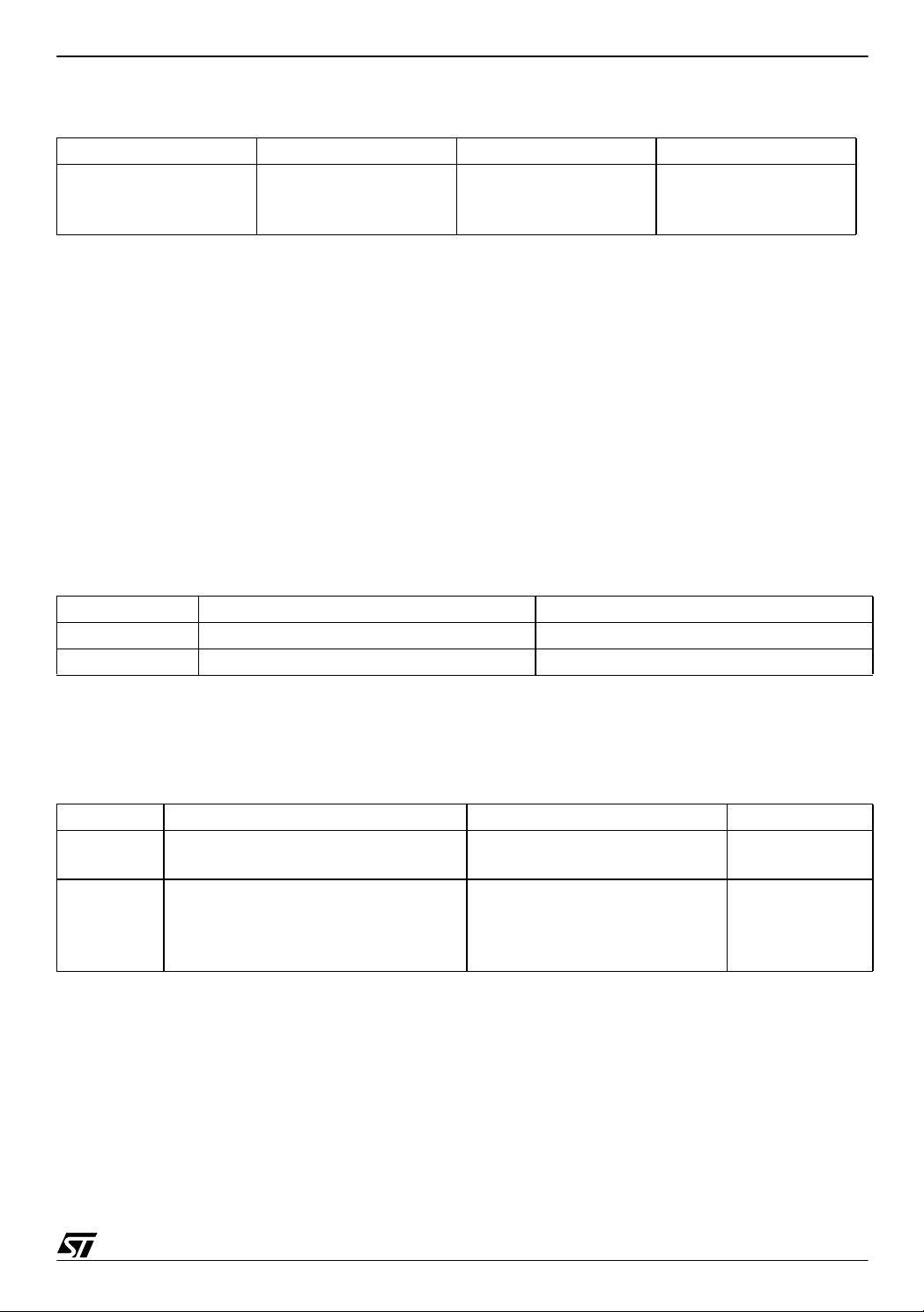
2.1.3 Absolute Electrical Sensitivity
This test is performed to assess the components immunity against destruction caused by
ESD.
Any devices that fails this electrical test program is classified as a failure.
Using automatic ESD tester, Electro-Static D ischarges (a positive then a negative pulse sep-
arated by 1 second) are applied to the pins of each sample according to each pin combination.
The sample size depends of the number of supply pi ns of the device (3 parts*(n+ 1): n= supply
pins). Two models are usually simulated: Human Body Model (HBM) and Machine Model
(MM). All parts are re-test ed on the production tester to veri fy the static and dynamic parameters still comply with the device datasheet (See Figure 6.).
This test co nforms to th e JES D22-A11 4A/A 115A s tandar d. See Figure 6. and the following
test sequences.
11/38
Page 12
EMC DESIGN GUIDE FOR ST MICROCONTROLLERS
Figure 6. Absolute Electrical Sensitivity test models
HIGH VOLTAGE
PULSE
GENERATOR
S1
R=1500W
CL=100pF
HUMAN BODY MODEL MACHINE MODEL
µC
HIGH VOLTAGE
S2
PULSE
GENERATOR
S1
CL=200pF
R=10k~10MW
µC
S2
2.1.3.1 Human Body Model Test Sequence
The HBM ESD pulse simulates the direct transfer of electrostatic charge, from the Human
Body, to a test device. A 100pF capacitor is discharged through a switching component and a
1.5 Kohm series resistor. This is currently the m ost reques ted industry model, for classifying
device sensitivity to ESD.
– C
is loaded through S1 by the HV pulse generator.
L
– S1 switches position from generator to R.
– A discharge from C
through R (body resistance) to the µC occurs.
L
– S2 must be closed 10 to 100ms after the pulse delivery period to ensure the µC is not left in
charge state. S2 must be opened at least 10ms prior to the delivery of the next pulse.
2.1.3.2 Machine Model Test Sequence
The MM ESD pulse em ulates the rapid direct transfer of electrostatic charge, from a charged
conductive object, such as a metallic tool or fixture, to a test device. This model consists of a
discharged 200pF capacitor, with no series resistor. The demand for MM ESD testing has increased, with the replacement of individual packaging by automated systems.
is loaded through S1 by the HV pulse generator.
– C
L
– S1 switches position from generator to the µC.
– A discharge from C
to the µC occurs.
L
– S2 must be closed 10 to 100ms after the pulse delivery period to ensure the µC is not left in
charge state. S2 must be opened at least 10ms prior to the delivery of the next pulse.
R (machine resistance), in series with S2, ensures a slow discharge of the µC.
Table 9 shows how HBM/MM ESD test results are presented in ST datas heets.
12/38
Page 13
EMC DESIGN GUIDE FOR ST MICROCONTROLLERS
Table 9. Example of HBM/MM ESD test results on ST72F521
Symbol Ratings Conditions
V
ESD(HBM)
V
ESD(MM)
Notes:
1. Data based on characterization results, not tested in production.
Electro-static discharge voltage
(Human Body Model)
Electro-static discharge voltage
(Machine Model)
T
=+25°C 2000
A
T
=+25°C 200
A
Maximum value
1)
Unit
V
2.2 ELECTROMAGNETIC INTERFERENCE ( EMI)
2.2.1 EMI radiated test This test correlates with the SAE J1752/3 standard.
This test gives a good evaluation of the contribution of the microcontroller to radiated noise in
an application environment. It takes into acco unt the MCU chip and also the package which
has a major influence on the noise radiated by the device.
Below is the package EMI contribution from the highest to the lowest:
SDIP/DIP
SOP
QFP
TQFP
The test is per for med in a Trans verse Elect romagn etic Mod e Ce ll (TEMCELL) w hich al lows
radiated noise measurement in two directions, rotating the test board by 90°
Test description:
The firmware running is based on a simple application, toggling 2 LEDs through the I/O ports.
The main directives for an SAE PCB are (Figure 8.):
– 100 x 100mm square board
– At least 2-layer board (ideally 4-layer).
– 5mm conductive edges on both sides connected to ground for contact with TEMCELL.
Figure 7. shows a typical example of an MCU EMC te st board sche m atics.
13/38
Page 14

EMC DESIGN GUIDE FOR ST MICROCONTROLLERS
Figure 7. Example of test board schematics for ST7
BP1
10k
LED 1
PB1
Xtal 1
Xtal 2
PB2
220
LED 2
220
+5v
PB3
VddA
Vdd1
Vdd2
Vdd3
100 nF
VssA
14/38
BP2
4.7k
GND
Reset
Vss1
Vss2
Vss3
GND
Vpp
10k
GND
Page 15

EMC DESIGN GUIDE FOR ST MICROCONTROLLERS
Figure 8. Test Printed Circuit Board specification according J1752/3 SAE st andard
15/38
Page 16

EMC DESIGN GUIDE FOR ST MICROCONTROLLERS
2.2.2 EMI level classification
The EMI classifications are dir ectly based on the absolute frequency and amplitude of the
emitted noise. Several international norms exist, based on different measurement methodologies, or emission levels, but the classification principle remains the same.
The standardized diagram (see Figure 9. ) is us efu l to get a s ynthes is a nd a cla ssification o f
EMI results, according to a standard framework. Each ST microcontroller EMI result is classified according to 4 SAE levels.
Figure 9. EMI level classification:
dbu V
60
Level 4
40
30
Level 3
Level 2
20
10
Level 1
0
-20
0.1 1 10 30 100 1000
MHz
Below is the potential risk associated with each EMI level:
_ higher than 4. high risk due to EMI level.
_ Level 4. may require cost for EMI compliance.
_ Level 3. moderate EMI risk.
_ Level 2. minimal EMI risk.
Table 10 shows how EMI test results are presented in ST datasheets.
for
Table 10. Example of EMI results
To give a synthetic view of the emi ssion sp ectrum, the highes t emiss ion level of 3 r anges of
ST72F521
frequency is indicated. EMI data are provided with relevant information such as the device
package and CPU frequency.
16/38
Page 17

EMC DESIGN GUIDE FOR ST MICROCONTROLLERS
3 ST MCU DESIG N STR ATEGY & EMC SPECIFIC FEATURE
At the initial specification of a new product, EMC dedicated features are implemented after an
identification of EMC constraints imposed by the MCU target applications. You should refer to
the specific product datasheet to know which of these feature described here are embedded.
Figure 10. Overview of specific features embedded in ST Microcontrollers
Low Power Oscillator
Multi Oscillator
Watchdog
(Firmware Management
refer to AN 1015)
I/O Protection
Controlled Slope
LVD/AVD
Embedded features
for EMC in
ST Microcontrollers
Internal Voltage Regulators
(For MCUs with low power core)
Internal PLL
3.1 SUSCEPTIBILITY
3.1.1 Low Voltage Detector (LVD)
The purpose of the LVD is to ensure that the Microcontroller will always work in its safe operating area (see Figure 12.). In terms of EMS, the presenc e of the LVD makes the M CU more
robust, ensuring that if any outside disturbance affects the power supply, the application can
recover safely.
When V
is below the « Min Working VDD» the behaviour of the Microcontroller is no longer
DD
guarantee d. There is no t enough power to decode/ execut e the instruc tions an d/or read the
memory. When V
is below the LVD level the M icrocontr oller enters in reset state (in ternal
DD
reset High) in order to prevent unpredi ctable behaviour . There are 2 level s with 25 0mV h ysteresis in order to avoid oscillating when the micro restarts. When a LVD reset occurs, a bit is
set by HW. This bit can be used to recover an application.
The Low Voltage Det ector func tion genera tes a static rese t when the V
below a V
reference value. This means that it secures the power-up as w ell as the power-
IT-
supply voltage is
DD
down keeping the Microcontroller in reset.
17/38
Page 18

EMC DESIGN GUIDE FOR ST MICROCONTROLLERS
The V
reference value for a voltage drop is lower than the V
IT-
reference value for power-on
IT+
in order to avoid a parasitic r eset when the MCU starts running and si nks current on the supply
(hysteresis).
The LVD Reset circuitry generates a reset when V
–V
when VDD is rising
IT+
–V
when VDD is falling
IT-
is below:
DD
The LVD function is illustrated in Figure 11..
The voltage threshold can be configured by option byte to be low, medium or high.
Provided the minimum V
value (guaranteed for the oscillator frequency) is above V
DD
IT-
, the
MCU can only be in two modes:
– under full software control
– in static safe r eset
In these conditions, secure operation is always ens ured for the application without the need
for external reset hardware.
During a Low Voltage Detector Reset, the RESET pin is held low, thus permitting the MCU to
reset other devices.
Notes:
The LVD allows the device to be used without any external RESET circuitry.
The LVD is an optional function which can be selected by option byte. Refer to product spec-
ification.
Figure 11. Low Voltage Detector vs Reset
V
DD
V
hys
V
IT+
V
IT-
RESET
18/38
Page 19

EMC DESIGN GUIDE FOR ST MICROCONTROLLERS
Figure 12. Max. Operating frequency vs. supply voltage.
16Mhz
8Mhz
Freq.
LVD low
LVD med.
Safe 8Mhz
area
LVD high
Safe 16MHz
area.
3.5V Reset
issued
Absolute working
window
Safe 16Mhz
area
3.8V Reset
issued
Vsupply
The minimum value of each supply range is l i mited by the LVD threshold which can be confi gured at one of three levels (low, medium or high) depending on the application.
3.1.2 Auxiliary Voltage Detector (AVD)
Like the LVD, this feature improves EMS performance by ensuring that the microcontroller behaves safely when the power supply is disturbed by external noise.
The AVD feature can be use d only if the LVD is acti vated. AV D has also differen t levels
(around 200mV above LV D le vels), enabling a early warning before t he reset c aused by the
LVD. Then, when AVD threshold is crossed, an interrupt is generated, requesting for example
some user a ction or prepar ing th e applic ation t o shut do wn in the i nterru pt routi ne unti l the
power supply returns to the correct level for the device (refer to the product datasheet).
Example: If f
The Voltage Detector func tion (AVD ) is b ased on an analog c ompariso n between a V
V
reference value and the VDD main supply. The V
IT+
lower than the V
is between 8 MHZ and 16 MHZ the min. working level is 3.5 volt.
CPU
reference value for falling voltage is
IT-
reference value for ris ing volt age in or der to avoid par asitic detecti on (hys-
IT+
IT-
and
teresis).
The output of the A VD c omparator is directly readable by the a pplication softw are th rough a
real time status bit (VDF). This bit is read only.
The AVD voltage thres hold value is rela tive to t he selected LVD thre shold configured b y op-
tion byte (see Microcontroller spec).
19/38
Page 20

EMC DESIGN GUIDE FOR ST MICROCONTROLLERS
If the AVD interru pt is enable d, an interr upt is gen erated when the vo ltage cros ses the
V
IT+(AVD)
or V
IT-(AVD)
threshold (AVDF bit toggles).
In the case of a drop in voltage, the AVD interrupt acts as an early warning, allowing software
to shut down safely before the LVD resets the microcontroller. (See Figure 13.).
The interrupt on the rising edge is used to inform the application that the V
warning state is
DD
over.
If the voltage rise time t
of the Microcontroller), no AVD interrupt will be generated when V
is greater than 256 or 4096 cycles then:
If t
rv
– If the AVD interrupt is enabled before the V
is less than 256 or 4096 CPU cycles (depending on the reset del ay
rv
is reached.
IT+(AVD)
IT+(AVD)
threshold is reached, then 2 AVD interrupts will be received: the first when the AVDIE bit is set, and the second when the threshold
is reached.
– If the AVD interrupt is enabled after the V
IT+(AVD)
threshold is reached then only one AVD
inte rrupt will occur.
Figure 13. Using the AVD to Monitor V
V
DD
DD
Early Wa rn in g Interru pt
(Power has droppe d, MCU not
not yet in reset)
V
V
IT+(AVD)
V
IT-(A VD)
V
IT+(LVD)
hyst
20/38
V
IT-(LVD)
AVDF bit 0 0RESET VALUE
AVD IN TERRUPT
REQUEST
IF AVDIE b it = 1
INTERRUPT PROCESS
LVD RESET
t
VOLTAGE RISE TIME
rv
11
INTERRUPT PROCESS
Page 21

EMC DESIGN GUIDE FOR ST MICROCONTROLLERS
3.1.3 I/O Features & properties
Although i nteg r ated c irc uit da ta she et s p r ovi de t he u se r with c on serv at ive limi ts an d con di tions in order to prevent damage, sometimes it is useful for the hardware system designer to
know the internal failure mechanisms: the risk of exposure to illegal voltages and conditions
can be reduced by smart protection design.
It is not possible to classify and to predict al l the possible damage resulting from violating maximum ratings and conditions, due to the large nu mber of v ariables th at come in to play in de fining the failures: in fact, when an overvoltage condition is applied, the effects on the device
can vary signi ficantly d epending on lot-to -lot proces s variatio ns, ope rating tempe ratu re, external interfacing of the Microcontroller with other devices, etc.
In the following sections, background technical information is given in order to help system designers to reduce risk of damage to the Microcontroller device.
3.1.3.1 Electrostatic Discharge and Latch-up
CMOS integrated circuits are generally sensitive to exposure to high voltage static electricity,
which can induce permanent damage to the device: a typical failure is the breakdown of thin
oxides, which causes high leakage current and sometimes shorts.
Latch-up is another typical phenomenon occurring in integrated circuits: unwanted turning on
of parasitic bipolar structures, or silicon-controlled rectifiers (SCR), may overheat and rapidly
destroy the de vice. Th ese unintent ional str uctures are compos ed of P and N regions wh ich
work as emitters, bases a nd collectors of parasitic bipolar transistors : the bulk resistance of
the silicon in the wells and substrate act as resistors on the SCR structure. Applying voltages
below V
or above VDD, and when the level of current is able to generate a voltage drop
SS
across the SCR parasitic resistor, the SC R may be turned on; to turn off the SCR it is necessary to remove the power supply from the device.
ST Microcontroller design implements layout and process solutions to decrease the effects of
electrostatic discharges (ESD) and latch-up. Of course it is not possible to test all devices, due
to the destructive nature of the mechanism; in order to guarantee product reliability, destructive tests are carried out on groups of devices, according to STMicroele ctronics internal
Quality Assurance standards and recommendations (see 2.1.2 Latch-Up (LU)).
21/38
Page 22

EMC DESIGN GUIDE FOR ST MICROCONTROLLERS
3.1.3.2 Protective Interface
Although ST Microcontroller input/output circuitry has been designed taking ESD and Latchup problems into account, for those a pplications and s ystems where ST Micr ocontroller pins
are exposed to illegal voltages and high current injections, the user is strongly recommended
to implement hardware solutions which reduce the risk of damage: low-pass filters and clamp
diodes are usually sufficient in preventing stress conditions.
The risk of having out-of-range voltages and currents is greater for those signals coming from
outside the system, where noise effect or uncontrolled spikes could occur with higher probability than for the internal signals; it must be underlined that in some cases , adopti on of filters
or other dedicated interface circuitries might affect global microcontroller performance, inducing undesired timing delays, and impacting the global system speed.
Figure 14. Digital Input/Output - Push-Pull
I/O CIRCUITRY
PIN
ESD PROTECTION
CIRCUITRY
P
OUTPUT
BUFFER
N
P
EN
PORT CIRCU ITRY
EN
P
INPUT
BUFFER
N
N
P
22/38
Page 23

EMC DESIGN GUIDE FOR ST MICROCONTROLLERS
3.1.3.3 Internal Circuitry: Digital I/O pin
Figure 14. shows a schematic representation of an ST Microcontroller pin able to operate ei-
ther as an input or as an output is shown. The circuitry implements a standard input buffer and
a push-pull configuration for the output buffer. It is evident that al though it is possible to disable
the output buffer when the input section is used, the MOS transistors of the buffer itself can still
affect the behaviour of the pin when exposed to illegal conditions. In fact, the P-channel transistor of the output buffer implements a di rect di ode to V
to the pin and N-well connected to V
a diode to V
(P-substrate connected to VSS and N-diffusion of the drain connected to the
SS
), while the N-channel of the output buffer implements
DD
(P-diffusion of the drain connected
DD
pin). In par allel to the s e di ode s, d edic ated c ircuitr y is impl em ent ed to p rote ct the logi c f rom
ESD events (MOS, diodes and input series resistor).
The most important characteristic of these extra devices is that the y must not di sturb normal
operating mod es, while acti ng during exp osure to ov er limit conditi ons, avoiding permane nt
damage to the logic circuitry.
According to t he MCU u sed, som e I/O pins can be prog ramm ed t o wo rk also as o pen-dr ain
outputs, by simply writing in the corresponding register of the I/O Port. The gate of the Pchannel of the output buffer is disabled: it is important to highlight that physically the P-channel
transistor is still present, so the diode to V
voltage applied to the pin is higher than the V
works. In some applications it can occur that the
DD
value (supposing the external line is kept
DD
high, while the Microcontroller power supply is turned off): this condition w ill inject curren t
through the diode, risking permanent damages to the device.
In any case, programm ing I/O pins as open-drain can help when several pins in the system
are tied to the same point: of course software must pay attention to program only one of them
as output at any time, to avoid output driver contentions; it is adv isabl e to configure these pins
as output open-drain in order to reduce the risk of current contentions.
23/38
Page 24

EMC DESIGN GUIDE FOR ST MICROCONTROLLERS
Figure 15. Digital Input/Output - True Open Drain Output
I/O CIRCUITRY
PIN
ESD PROTECTION
CIRCUITRY
OUTPUT
BUFFER
N
EN
P
N
EN
PORT CIRCUITRY
INPUT
BUFFER
N
P
In Figure 15. a true open -dra in pin s chem atic i s s hown. In this c as e all pa ths to V
are re-
DD
moved (P-cha nne l dr iv er, E SD p rote cti on dio de, i nter nal w eak pul l-up ) i n or der to a llow t he
system to turn off the power supply of the microcontroller and keep the voltage level at the pin
high without injecting current in the device. This is a typical condition which can occur when
several devices interface a seri al bus: if one device is not i nvolved in the communication, it can
be disabled by turning off its power supply to reduce the system current consumption.
When an illegal negative voltage level i s appli ed to the Microcontroller I/O pi ns (both versions,
push-pull and true open-drain output) the clamp diode is always present and active (see ESD
protection circuitry and N-channel driver).
24/38
Page 25

EMC DESIGN GUIDE FOR ST MICROCONTROLLERS
3.1.3.4 Internal Circuitry: Analog Input pin
Figure 16. shows the internal circuitry used for analog input. It is primarily a digital I/O with an
added analog m ultiplexer for the sel ection of the input cha nnel of the Analog to Digital Con verter (ADC).
The presence of the multiplexer P-channel and N-channel can affect the behaviour of the pin
when exposed to illegal voltage conditions. These transistors are controlled by a low noise
logic, biased through AV
and AVSS including P-channel N-well: it is important to always
DD
verify the input voltage value with respect to both analog power supply and digital power
supply, in order to avoid uni ntentional current injections which (i f not limited) could destroy the
device.
Figure 16. Digital Input/Output - Push-Pull Output - Analog Multiplexer Input
I/O CIRCUITRY
P
PIN
E
SD PROTECTION
CIRCUITRY
OUTPUT
BUFFER
N
P
EN
N
P
N
N
EN
P
INPUT
BUFFER
P
PORT CIRCUITRY
P
25/38
Page 26
EMC DESIGN GUIDE FOR ST MICROCONTROLLERS
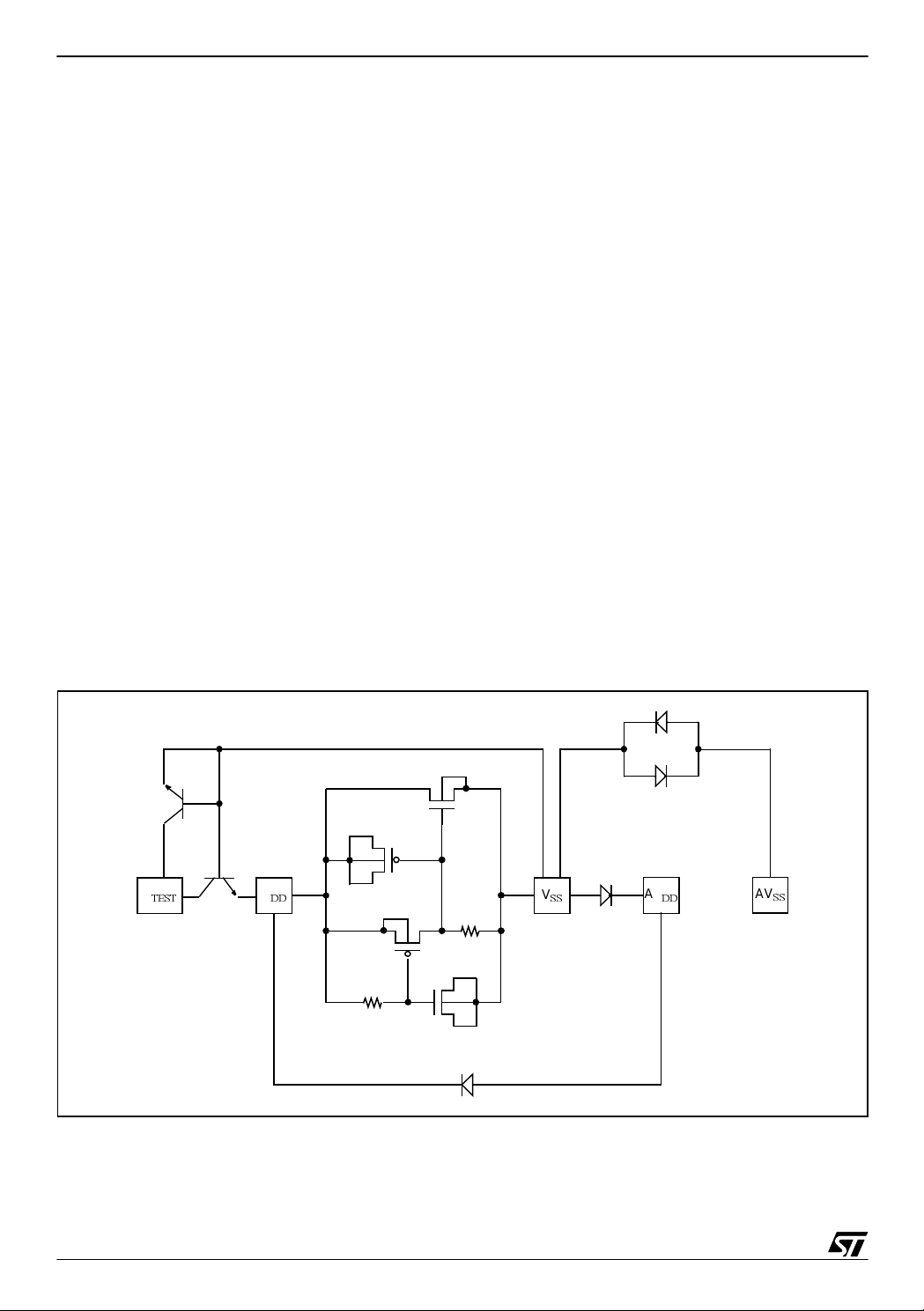
3.1.4 Multiple VDD & VSS.
As already said for the I/O pins, in order to ens ure ST Microcontroller c ompliance with respect
to Quality Assurance recommendations concerning ESD and Latch-up, dedicated circuits are
added to t he differ ent pow er suppl y and gro und pi ns (digit al and an alog). T hese s tructure s
create preferred paths for the high curr ent injected duri ng discharges, avoiding damage to active logic and circuitry. It is important for the system designer to take this added circuitry into
account, when applying different current levels and voltages to the power supply and ground
pins. Figure 17. shows schematically the protection net implemented on ST Microcontroller
devices, composed of diodes and other special structures.
The clamp structure between the V
and VSS pins is designed to be active during very fast
DD
transitions (typical of electrostatic discharges). Other paths are implemented through diodes:
they limit the possibi lity of pos itively differenti ating AV
considerations are valid for AV
and VSS due to the back-to-back diode structure imple-
SS
mented between the two pins. Anyway, it must be highlighted that, because V
and VDD (i.e . A VDD > VDD); similar
DD
and AVSS are
SS
connected to the sub strate o f the silicon die (even though in d ifferent areas o f the die itself),
they represent the reference point from which all other voltages are measured, and it is recommended to never differentiate AV
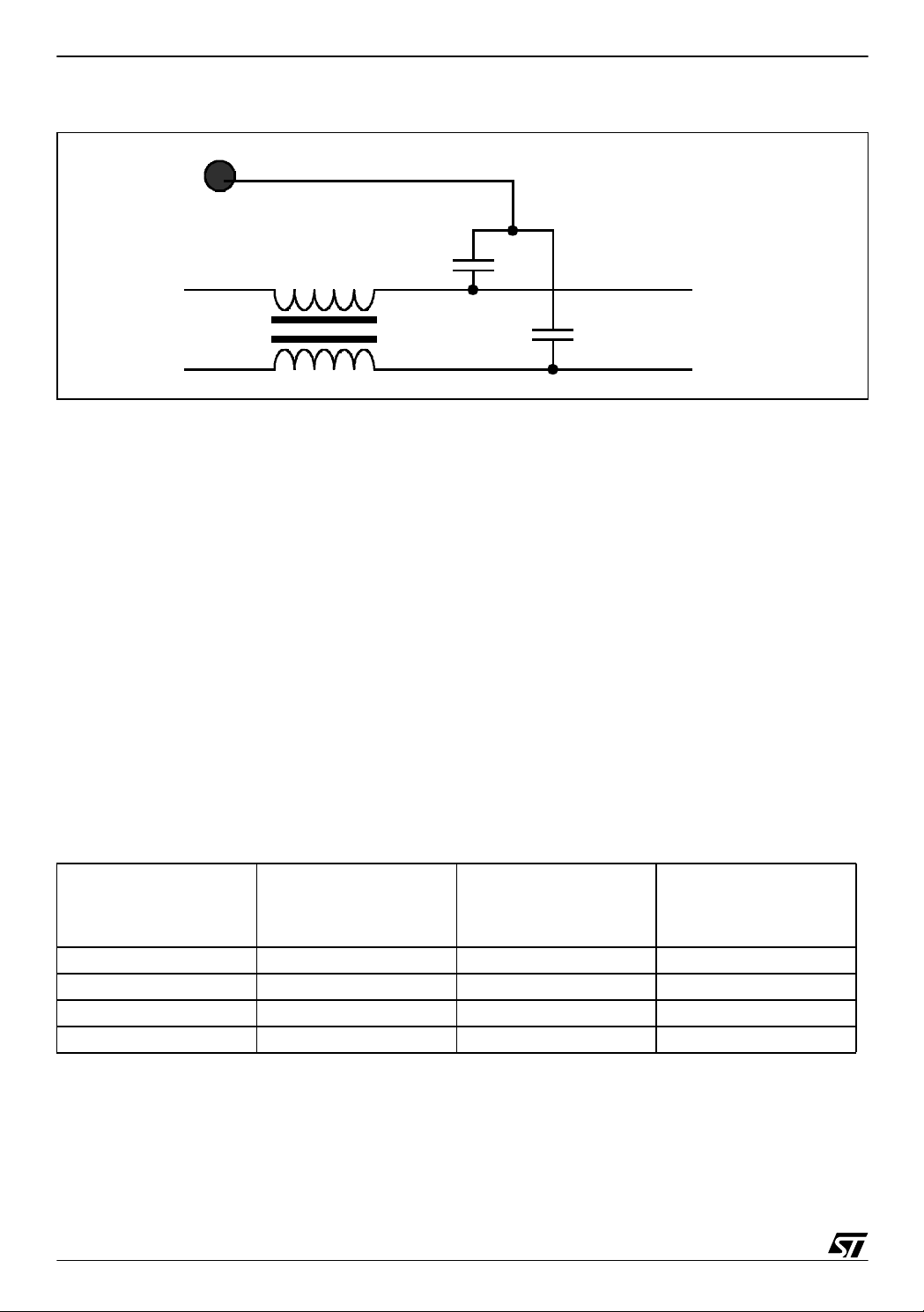
Note: If m ore than one pair of pins for V
from VSS.
SS
SS
and VDD is available on the device, they are con-
nected internally and the protection net diagram remains the same as shown in Figure 17..
Figure 17. Power Supply and Ground Configuration (on ST9)
N
P
26/38
V
TEST
V
DD
P
N
V
SS
AV
DD
AV
SS
Page 27

EMC DESIGN GUIDE FOR ST MICROCONTROLLERS
3.2 EMISSION
3.2.1 Internal PLL
Some ST Microco ntrollers have a n embe dded program mab le PLL Clock Gener ator allowing
the usage of standard 3 to 5 MHz crystals to obtain a l arge range of internal frequencies (up
to 24MHz). By these means, ST Microcontroller can operate with cheaper, medium frequency
crystals, while still providing a high frequency internal clock for maximum system performance. The high clock frequency source i s contained inside the c hip and does not go thr ough
the PCB (Printed Circuit Board ) tracks and external com ponents. This reduce s the potential
noise emission of the application.
The use of PLL network also filters CPU clock against external sporadic disturbances
(glitches) .
3.2.2 Global low power approach
3.2.2.1 Low powered oscillator
The oscillator is an major source of noise. To reduce this noise emission, the current driven by
the oscillator is limited.
The main clock of some of ST Microcontrollers can be generated by four different source types
coming from the multi-oscillator block (MO). This allows the designer to easily select the best
trade-off in terms of cost, performance and noise emission. The clock sources are listed below
in order from the most noisy to the least noisy:
■ an external source
■ crystal or ceramic resonator oscillators
■ an internal high frequency RC oscillator
Each osc illat or is o ptimi zed fo r a giv en fre que ncy ran ge in t erm s of cons um ption an d is se lectable through the option byte. The associated hardware configurations are shown in Table
11. Refer to the electrical characteristics section of the datasheet for more details in each
case.
External Clock Source
In external clock mode, a clock signal (square, sinus or triangle) with ~50% duty cycle has to
drive the OSC1 pin while the OSC2 pin is tied to ground.
Crystal/Ceramic Oscillators
This family of oscillators has the advantage of producing a very accurate rate on the ma in
clock of the microcontroller. The selection within a list of 5 os cillators with different frequency
ranges has to be done by option byte in order to reduce consumption (refer to the Microcontroller datasheet for more details on the frequency ranges). In this mode of the multi-oscillator,
the resonator and the load capacitors have to be placed as c lose as possible to the oscillator
27/38
Page 28

EMC DESIGN GUIDE FOR ST MICROCONTROLLERS
pins in order to minimize output distortion and start-up stabilization time. The loading capacitance values must be adjusted according to the selected oscillator.
These oscillators are not stopped during the RESET phase to avoid the del ay needed for the
the oscillator start-up.
Internal RC Oscillator
The internal RC osci llator is the most c ost ef fective s oluti on, with the draw back of lower frequency accuracy. Its frequency is in the low single digit MHz range. In this mode, the two oscillator pins have to be tied to ground.
Process variations will also bring some differences from lots to lots (20 to 60%).
Some S T Mic roc ontr oller s (ref er to p rodu ct sp ecif icat ion) em bed a pro cess c omp ens ation .
This feature is called “Tri mmable internal RC”. A procedure duri ng test operati on anal yzes the
process variation and calibrate the internal oscillator accordingly. This brings the internal RC
accuracy to 1%. This procedure can be also performed by the user:
Refer to AN1324 “Calibrating the RC oscillator of the ST7FLITE0 using the mains”
Table 11. ST7 Clock Sources
Hardware Configuration
ST7
OSC1 OSC2
R
EX
OSC1 OSC2
ST7
C
EX
External Clock
Crystal/Ceramic Resonators
OSC1 OSC2
EXTERNAL
SOURCE
OSC1 OSC2
C
L1
CAPACITORS
ST7
ST7
LOAD
External RC Oscillator
C
L2
Internal RC Oscillator
The ST mu lti-os cillator s y stem i s de signe d f or f lexibility an d to a llow the s ystem des igner to
find the best compromise between emission, accuracy and cost criteria.
28/38
Page 29

EMC DESIGN GUIDE FOR ST MICROCONTROLLERS
3.2.2.2 Internal Voltage Regulators (for M CUs with low power core).
An internal Voltage Regulator is used to power some ST Microcontrollers Cores starting from
the external power supply.
The Voltage Regulator reduces EMI due to the MCU Core with 2 effects:
– Lower CPU Supply Voltage
– Isolate CPU Supply from external MCU supplies.
3.2.3 Output I/O Current limitation & edge timing control
Output buffers are embedded in ST Microcontrollers, their switching speed is controlled in
order to avoid parasitic oscillations when they are switched. The MCU design makes a tradeoff between noise and speed.
29/38
Page 30

EMC DESIGN GUIDE FOR ST MICROCONTROLLERS
4 EMC GUIDELINES FOR MCU BASED APPLICATIONS
The following guidelines result from experience gained in a wide variety of applications.
4.1 HARDWARE
The major noise receptors and generators are the tracks and wiring on the Printed Circuit
Board (PCB), especially those near the MCU. The first actions to prevent noise problems thus
concern the PCB layout and the design of the power supply.
In general, the smaller the number of components surrounding the MCU, the better the immunity versus noise. A ROMless solution, for instance, is typically more sensitive to and a bigger
generator of noise than an embedded memory circuit.
Optimized PCB layout
Noise is basically r eceived and transm itte d throu gh track s and comp onents wh ich, o nce excited, act as antennas. Each loop and track includes parasitic inductance and capacitance
which radiate and absorb energy once submitted to a variation of current, voltage or electromagnetic flux.
An MCU chip itself presents high immunity to and low generation of EMI since its dimensions
are small versus the wave lengths of EMI signals (typically mm versus 10's of cm for EMI signals in the GHz range). So a single chip solution with small loops and short wires reduces
noise problems.
The initial action at the PCB level is to reduce the number of possible antennas. The loops and
wires connec ted to the M CU s uch as supply, os cillator an d I /O s hould be cons idere d with a
special attention . The osc illator loop ha s to be especially sma ll si nce it o perate s at hig h frequency Figure 18.
A reduction of both the inductance and the c apacitance of a track i s gener ally difficult. Prac tical experience suggests that in most cases the inductance is the first parameter to be minimized.
30/38
Page 31

EMC DESIGN GUIDE FOR ST MICROCONTROLLERS
Figure 18. PCB Board Oscillat or Layout Examples
The reduction of inductance can be obtained by making the lengths and surfaces of the track
smaller. This can be obtained by placing the track loops closer on the same PCB layer or on
top of one another (Figure 19.). The resulting loop area is small and the electromagnetic fields
reduce one another.
The ratio in order o f ma gnitude relat ing to the inductanc e va lue a nd the a re a de fined b y the
wire loop is around 10nH/cm2. Typical examples of low inductivity wires are coaxial, twisted
pair cables or mul tiple lay er PCBs with one gr ound and one s upply layers. T he curr ent dens ity
in the track can also be smaller due to track enlargement or the paralleling of several small capacitances mounted in the current flow.
In critical cases, the distance between the MCU and the PCB, and therefore the surfaces of
the loops betwee n an MCU and its env ironment, has also to be minimize d. This can be
achieved by removing any socket between the MCU package and the PCB, by replacing a ceramic MCU package by a plastic one or by using Surface Mounting instead of Dual In Line
packages.
Note: Board vias are inductances. Try to avoid them. If needed, use multi vias.
31/38
Page 32

EMC DESIGN GUIDE FOR ST MICROCONTROLLERS
Figure 19. Reduction of PCB Tracks Loop Surfaces
High Inductance
Low Inductance
Note: T his test is done with a double sided PCB. Insulator thickness is 1.5mm, copper thick-
ness is 0.13mm. The overall board size is 65 x 200mm.
Power supply filtering
The power supply is used by all parts of the circuit, so it has to be considered with special attention. The supply loops have to be decoupled to make sure that signal levels and power currents do not i nterfere. Thes e loops c an b e sepa rated using star wiring wi th one node des ignated as common for the circuit (Figure 20.).
The decoupling capacitance should be placed very close to the MCU supply pins to minimize
the resultant loop. It should be also large enough to absorb, without significant voltage increase, parasitic currents coming from the M CU via the input protection diode s. The decoupling of the board can be done with electrolytic capacitors (typ. 10µF to 100µF) since the dielectric used in such capacitors provides a high volumic capacitance. However these capacitors behave like induc tances at high fr equency (ty p. above 10M Hz) while ceram ic or plastic
capacitors keep a capacitive behaviour at higher frequency. A c eramic capacitance of, for instance, 0.1µF to 1µF should be used as high frequency supply decoupling for critical chips operating at high frequency.
32/38
Page 33

EMC DESIGN GUIDE FOR ST MICROCONTROLLERS
Figure 20. Power Supply Lay-out Examples
I/O configuration
An open (floating) pin is a potential hazard to the circuit.
I/O pins whic h a re n ot used i n the ap plic ation shou ld b e pr efera bly confi gure d in output low
state. This will also minimize the current consumption.
A major source of emission in Microcont roller bas ed applicat ions can be du e to high spe ed
digital I/O and commu nic ation in terfaces s uch as SPI, I2C c locks, U SB or P WM... Th e Rise/
Fall times are critical. Typical designs add RC low pass filters.
Shielding
Shielding can help in reducing noise sensitivity and emission, but its success depends directly
on the material chosen as shield (high permeability, low resistivity) and on its connection to a
stable voltage source including a decoupling capacitance via a low serial impedance (low inductance, low resistance).
If the generator of major disturbances is near to the MCU board and can be identified as a
strong dV/dt generator (i.e. a transformer or Klystron), the noise is carried mainly by the electrostatic field. The critical coupling between the noise generator and the control board is capacitive. A highly conductive shield (i.e. copper) creating a Faraday cage around the control
board may strongly increase the immunity.
33/38
Page 34

EMC DESIGN GUIDE FOR ST MICROCONTROLLERS
If the strongest source of perturbations is a dI/dt generator (i.e. a relay), it is a high source of
electromagnetic fields. Therefore, the permeability of the s hielding ma terial (i.e. alloy) is crucial to increase the immunity of the board. In addi tion, the number and size of the hol es on the
shield should be reduced as much as possible to increase its efficiency.
In critical cases, the implantation of a ground plane below the MCU and the removal of sockets
between the device and the PCB can reduce the MCU noise sensitivity. Indeed, both actions
lead to a reduction of the apparent surface of loops between the MCU, its supply, its I/O and
the PCB.
4.2 HANDLING PRECAUTIONS FOR ESD PROTECTION.
Electronic components have to be protected fr om the hazard of static electricity from the manufacturing stage down to where they are utilized in order to avoid ESD related destruction. A
specific no-compromise strategy is implemented at ST for all ESD sensitive products.
From the wafer level to the shipping of finished goods, each workstation and processing step
is guaranteed. For final packing, ST uses anti -static tubes . This solution ensures full ESD protection of devices. However, the supplier's greatest efforts are in vain if the end user does not
provide the same level of protection and care in the application.
A relative humidity of 50% to 65% is the best to prevent el ectrostatic problems (the lower the
relative humidity, the higher the electrostatic voltage). Nevertheless, the person handling the
semiconductors as well as the equipment will be charged to a certain level. T he work environment is very important to protect devices against static electricity
Anti-static electricity measures during work
(1) Conductive mat
(2) Wrist
(3) Conductive floor mat
(4) Work suit with anti-static measure
(5) Conductive shoes grounding the human body
34/38
Page 35

EMC DESIGN GUIDE FOR ST MICROCONTROLLERS
Figure 21. Grounding the Human Body
(1) Wrist ring
(2) Grounding wire: threaded copper wire, vinyl covered, about 1 meter
(3) 250 KW to 1 MW resistance is built in
Device handling:
Static control wrist straps, used and connected properly, must be worn.
All tools, persons, testing machines, which could come in contact with device leads, must be
conductive and gr ounded. Each tabletop mu st be protected with a cond uctive mat , properly
grounded. Use static control shoe strap. Use vacuum pipes.
Storage box:
Keep parts in the original packing bags up to the very last moment of the production line.
If bigger containers ar e used for i n-plant transport of dev ices or PC boards, they must be elec-
trically conductive like the carbon-loaded types. Avoid use of high dielectric materials (like polystyrene) for sub-assembly construction, storing, and transportation.
35/38
Page 36

EMC DESIGN GUIDE FOR ST MICROCONTROLLERS
Equipment and tools:
Use Ionized air blowers to neutralize static charges of non-conductive materials.
Use only the grounded tip variety of soldering iron.
Use proper power supply systems in testing and application.
Supply voltage should be applied before and removed after input signals.
Insertion and remova l of component s from sockets sh ould be carried out with no po wer ap-
plied .
An open (floating) pin is a potential hazard to the circuit. Each “Non Connected” pin should be
grounded or connected to V
through a resistor whenever possible.
DD
4.3 FIRMWARE
This part is Treated by a dedicated Application Note (AN1015) available on ST Website.
4.4 WEB LINKS TO EMC RELATED ORGANISATIONS
FCC: Federal Communication Commission
http://www.fcc.gov
EIA: Electronic Industries Alliance
http://www.eia.org/
SAE: Society of Automotive Engineers
http://www.sae.org
IEC: The International Electrotechnical Commission
http://wwwiec.ch
CENELEC: European Committee for Electrotechnical Standardisation
http://ww.cenelec.be
JEDEC: Joint Electron Device Engineering Council
http://www.jedec.org
36/38
Page 37

EMC DESIGN GUIDE FOR ST MICROCONTROLLERS
5 CONCLUS ION
For any microcontroller application, EMC requirements must be considered at the very beginning of the developm en t project. Standar ds, featu res an d param eters g iven i n ST Microcon troller datasheets will help the system designer to determine the most suitable component for
a given a pplic atio n. Ha rdw a re and fi rmw are precau ti on s h av e to b e ta ke n to o pt im ize E M C
and system stability.
37/38
Page 38

EMC DESIGN GUIDE FOR ST MICROCONTROLLERS
“THE PRESENT NOTE WHICH IS FOR GUIDANCE ONLY AIMS AT PROVIDING CUSTOMERS WITH INFORMATION
REGARDING THE IR PRO DUCT S IN OR DER FO R THEM TO SAV E TIME . AS A RES ULT, STMIC ROEL ECTR ONI CS
SHALL NOT BE HELD LIABLE FOR ANY DIRECT, INDIRECT OR CONSEQUENTIAL DAMAGES WITH RESPECT TO
ANY CL AIM S AR IS IN G FR OM T HE CO N TENT OF S UC H A NO TE A ND /O R T HE U SE M AD E BY C US TO ME RS O F
THE INFORMATION CONTAINED HEREIN IN CONNECTION WITH THEIR PRODUCTS.”
Information furnished is believed to be accurate and reliable. However, STMicroelectronics assumes no responsibility for the consequences
of use of such information nor for any infringement of patents or other rights of third parties which may result from its use. No license is granted
by implic ation or otherwise under any patent or patent ri ghts of STM i croelectr oni cs. Spec i fications mentioned i n this publication are subje ct
to change without notice. This publication supersedes and replaces all information previously supplied. STMicroelectronics products are not
authorized for use as cri tical comp onents in life support dev i ces or systems wi thout exp res s written ap proval of STMi croelectr onics.
The ST logo is a registered trademark of STMicroelectr oni cs.
All other n am es are the pro perty of thei r respectiv e owners
© 2003 STMi croelectronics - All rights reserved
STMicroelectronics GROUP OF COMPANIES
Australi a – B elgium - Brazil - Canada - China – Czech Republ i c - Finland - F rance - Germany - Hong Kong - India - Is rael - Italy - Japan -
Malaysia - Malta - Morocco - Singapore - Spain - Sweden - Switzerland - United Kingdom - United States
www.st.com
38/38
 Loading...