

1 INTRODUCTION
APPLICATION NOTE
AN1707
TD220/221
Gate Driver wit h Vreg and Two-Point Regulator
by Giuseppe Scuderi
This application note gives a simple functional
description of the TD220/221, which is a standard
circuit designed with an industrial application in
mind, see
However, the TD220/221, together with other ST
components, such as an ST7 microcontroller, and
a MOSFET device, can provide a flexible, highperformance, power management solution that
may be broadly applied to applications in the
industrial fields.
A common problem in such off-line applications is
the generation of a low voltage power supply for
the various control ICs.
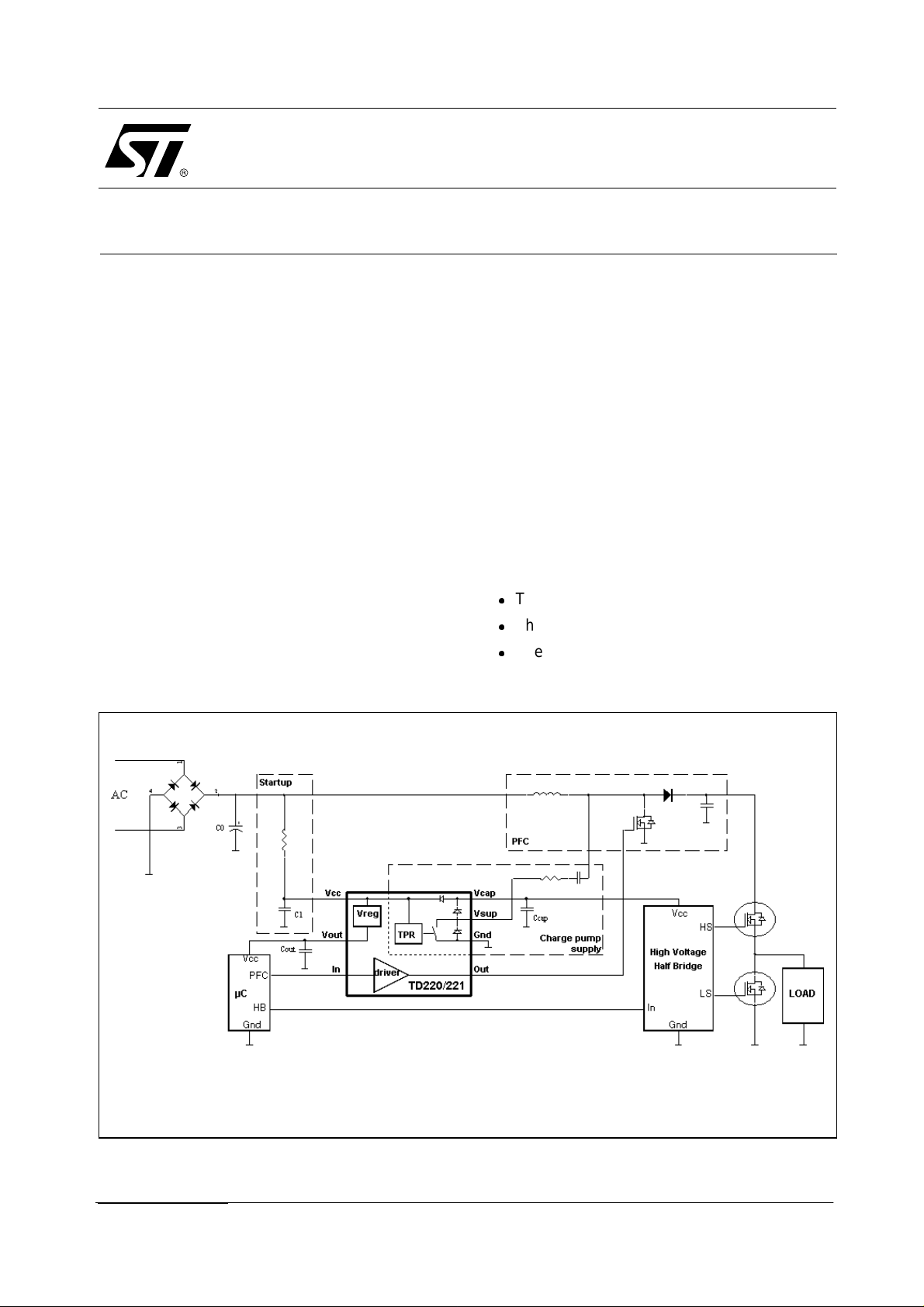
Fig. 1: Typical application schematic of the TD220/22
Figure 1
.
Because of this, the TD220/221 includes a
"Two-Point Regulator” that enables control of a
switching charge pump connected.
The charge pump diodes are integrated within the
TD220/221, and a switch disables the charge
pump when the nominal voltage is reached.
The main advantage of the TD220/221 is that it
integrates, in a single SO8 package, 3 block
functions—voltage regulation, power supply and
power MOS driver—at a very reasonable price.
In typical applications, the TD220/221 manages
the following functions:
l
The MOSFET gate driver.
l
The microcontroller’s 3.3 V or 5 V supply.
l
The power supply voltage at 13 V.
October 2003
Revision B 1/5
AN1707 Introduction
Fig. 2: Description of the TD220/221
As shown in
Figure 1
, the TD220/221 internal
blocks are:
l
Source—Used in order to bias other blocks in
the circuit,
l
UVLO—Under Voltage Lock Out,
l
Vreg—Voltage Regulator at 3.3 V (for the
TD220) or at 5 V (for the TD221),
l
Driver—Provides the current in order to
drive an external MOS,
l
TPR—Two Point Regulator,
l
Clamp—Fixes the maximum Vcc at 22 V.
The UVLO block insures that Vcc is set such that
the TD220/221 functions correctly. Two boundary
voltages are internally fixed at 14.1 V (UVLOH)
and at 8.2 V (UVLOL). If the circuit is in the OFF
state, it will turn on when the UVLO voltage
reaches 14.1 V. This represents the minimum
value necessary to turn the circuit ON, and then
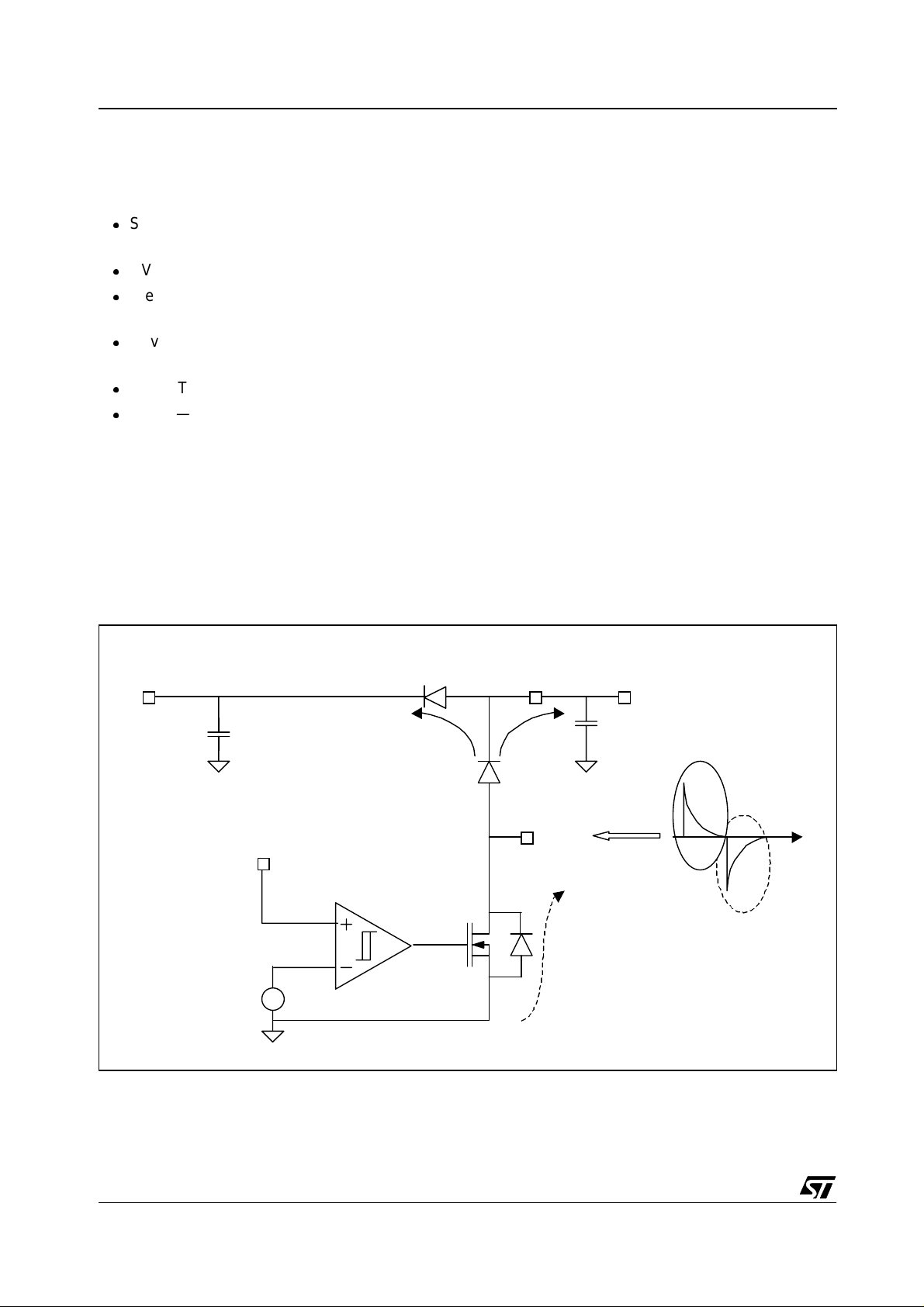
Fig. 3: TPR schematic: LDMOS Off
the Vcc power supply value stabilizes at 13 V.
When the circuit is in the ON state, maximum
UVLO voltage value that turns the circuit OFF is
8.2 V.
The role of the UVLO is both simple and
extremely important: it imposes the voltage range
for circuit ignition and blocking.
When the Vcc is at 13 V the Vreg b lock pr ovides a
precise output voltage at 3.3 V (for the TD220) or
at 5 V (for the TD221) with accuracy of ±3% at
25°C and for Iout = 10 mA. This Vcc is used to
supply power to the driver of an external power
MOS.
The Vcc voltage is so exact thanks to the TPR
block that allows it to maintain an accuracy of
±300 mV. This variation is measured using the
external capacitor C1 = 100 nF as shown in
Figure 3
and
Figure 4
.
VCC VCAP
C1
Threshol d Com pa rat or Hi gh = 13. 15V
Threshol d Com pa rat or Low = 12. 85 V
D1
D2
VSUP
VCC
LDMO S
13V
V
C2
Isup
t
2/5

Introduction AN1707
Fig. 4: TPR schematic: LDMOS On
VCC VCAP
C1
Threshol d Com pa rat or Hi gh = 13.15V
Threshol d Com pa rat or Low = 12 . 85 V
D1
D2
VCC
LDMO S
13V
V
The Vcc voltage is regulated by the power
LDMOS, driven by the CMOS comparator with
hysteresis.
Fig. 5: VSUP current behavior
VSUP
C2
Isup
t
When the LDMOS is in the OFF state, the energy
arrives at the VSUP pin, and the current passes
across the D1 and D2 diodes, charging the C1
and C2 capacitors, and increasing the Vcc voltage
value.
When the LDMOS is in the ON state, the energy
discharges versus the ground and the Vc c vol tage
value decreases with reference to the application
consumption.
As shown in
Figure 5
, it is possible to see the
current behavior on the VSUP pin. This behavior
is generated by an RC circuit supplied perio dically
with a duty cycle of 50%.
When the LDMOS is in the OFF state , the positi ve
current pulse charges C1 and C2 capacitors and
the negative current pulse goes across the
internal LDMOS diode.
When the TPR threshold reaches Vtpron, almost
13.15 V, the comparator switches the LDMOS to
the ON state.
In this case, the positive current pulse goes
across the LDMOS (Ron) and discharges to
ground, while the negativ e current p ulse is di vided
between the Ron and the internal diode.
When Vcc voltage reaches Vtproff, almost
12.85 V, the comparator turns off the LDMOS and
the current pulses charge the C1 and C2
capacitors again.
Figure 6
shows the above des cribed behavior for
the TD220/221 application.
3/5

AN1707 UVLO Start Up
2 UVLO START UP
The UVLO startup feature requires an off-line
voltage, together with a resistor, to be connected
to the Vcc pin, as shown in
Figure 1
The Vcc waveform at startup i s shown i n
on page 1.
Figure 7
You should study the charging and discharging
time of the C1 capacitor time in order to choose
the optimum value of C1 for your application. The
C1 value should insure a sufficient discharge
delay time to avoid reaching the UVLOL voltage
value (8.2 V) which would turn off the circuit
before the first current pulses arrive.
Fig. 7: UVLO Start Up and Ivsup
VCC
VCC
VCC
UVLOH = 14.1V
UVLOH = 14.1V
UVLOH = 14.1V
Fig. 6: VSUP and VCAP dynamic behavior
C1 and C2 charging time
C1 and C2 charging time
.
Vcc = 13V RMS (DC)
Vcc = 13V RMS (DC)
C1 and C2 dic ha rgi ng time
C1 and C2 dic ha rgi ng time
Vtpron = 13.15V
Vtpron = 13.15V
Vtpron = 13.15V
Vtproff = 12.85V
Vtproff = 12.85V
Vtproff = 12.85V
UVLOL = 8.2V
UVLOL = 8.2V
UVLOL = 8.2V
s
s
s
v
v
v
I
I
I
u
u
u
p
p
p
n
n
n
o
o
o
V
V
V
a
a
a
c
c
c
p
p
p
Choise of C1 for the
Choise of C1 for the
Choise of C1 for the
minimum margin
minimum margin
minimum margin
in order to guarantee
in order to guarantee
in order to guarantee
thecircuit ON state
thecircuit ON state
thecircuit ON state
4/5

AN1707 Conclusion
3 CONCLUSION
The TD220/221 has been designed for power
managment applications in the industrial fields.
This component integrates a Gate Driver with
Vreg and Two-Point regulator in an SO8 plastic
package. Good performance, excellent accuracy
and low cost characterize this product.
Information furnished is believed to be accurate and reliable. However, STMicroelectronics assumes no responsibility for the
consequen ces of use of such information no r for any i nf ring e men t of patents or other rights of thi r d par tie s whi ch may re su l t from
its use. No license is granted by implication or otherwise under any patent or patent rights of STMicroelectronics. Specifications
mentioned in this publication are subject to change without notice. This publication supersedes and replaces all information
previously supplied. STMicroelectronics products are not authorized for use as critical components in life support devices or
systems without express written approval of STMicroelectronics.
Australia - Brazil - China - Finland - France - Germany - Hong Kong - India - Italy - Japan - Malaysia - Malta - Morocco
The ST logo is a registered trademark of STMicroelectronics
© 2003 STMicroelectronics - All Rights Reserved
STMicroelectronics GROUP OF COMPANIES
Singapore - Spain - Sweden - Switzerland - United Kingdom
http://www.st.com
5/5
 Loading...