

Page 1
AN1696
APPLICATION NOTE
L6615, LOAD SHARE CONTROLLER FOR N+1
REDUNDANT, HOT-SWAPPABLE APPLICATION
by Luca Salati
Power supply systems are often designed by paralleling converters in order to improve performance or
reliability. To ensure uniform distribution of stresses, the total l oad current should be equally shared
among the converters.
This application note describes a redundant system (a demo board is available) composed by three paralleled DC-DC converter modules (synchronous buck t opology, managed by ST L6910) whose output
currents are shared through the new ST current sharing controller (L6615).
In this application it is shown the innovative use of a MOSFET as both OR-ing element (replacing ORing diode) and sensing element (R
Introduction
ds(ON
)).
Load sharing is a technique commonly used when powering loads requiring low voltage and high current; for
this reason a modular power system is built where two (or m ore) power supplies or DC -DC converters are paralleled and supply the load.
Sharing the output currents is useful to equalize the thermal stress of the different modules providing an advantage in terms of el ec troni c components rel iability (mean time between failure roughly doubles every 10°C decrease in operating temperature).
April 2003
1/11
Page 2
AN1696 APPLICATION NOTE
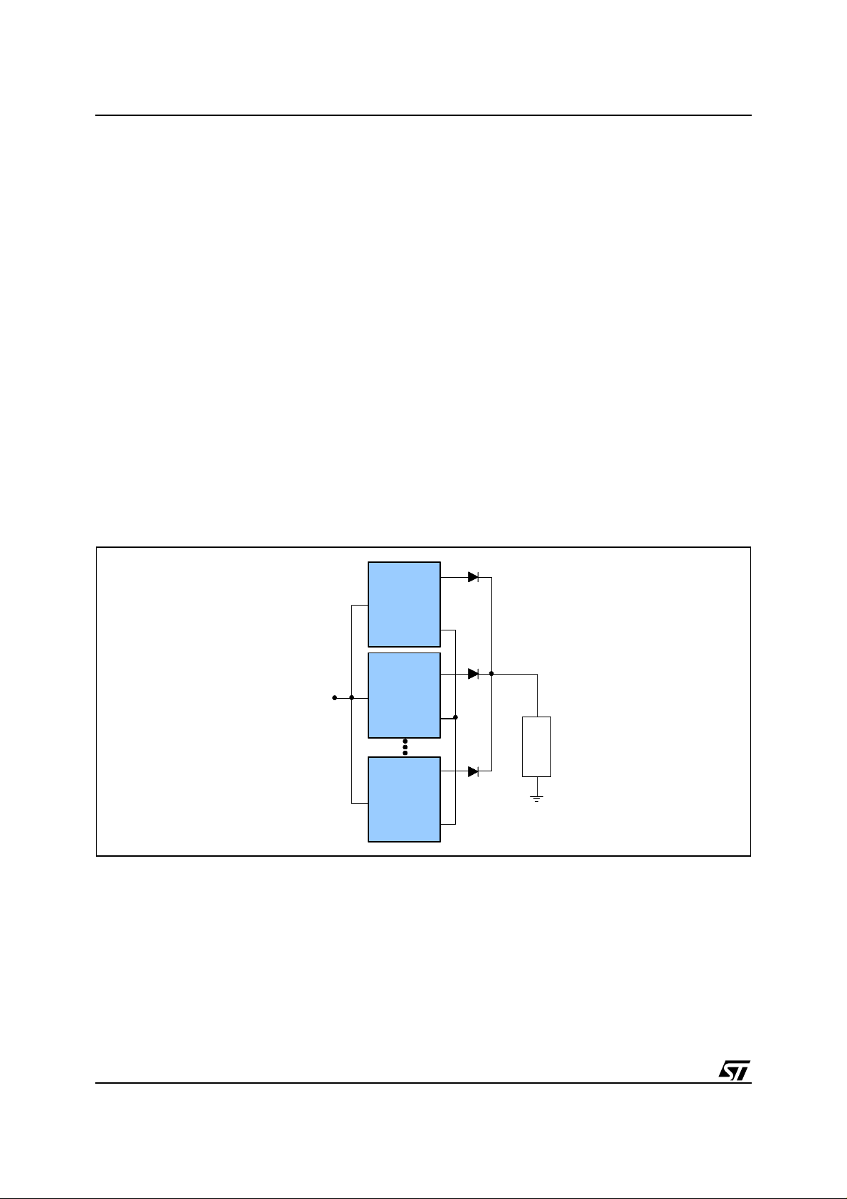
In this application, load sharing control is entrusted to ST's L6615 [1] that features automatic master-slave current sharing control [2] [3]: the supply that delivers the highest current (sensed by means of an external resistor)
acts as the master and drives a common reference (share bus ) t o a vol t age proporti onal to i t s out put c urrent;
the feedback voltage of the others parallel ed power s upplies (slaves) i s t hen tr i mmed by an "adjustment" network so that they can support their amount of load current. The slave supplies work as current-controlled current
sources.
Moreover a paralleled supply architecture allows achieving redundancy (a system of paralleled power supplies,
each delivering a current lower than its nomi nal capabil it y); the f ai l ure of one of the modules can be tol erat ed
until the capability of the remai ning power supplies i s enough t o provide the required load current. In thi s way
an interruptible power supply will be designed, reducing the failure rate of the output bus.
In hot-swappable applications, whenever a section fails, it has to be removed and replaced without turning off
the system and causing significant perturbation to both input and output system buses.
At insertion, each sect i on exhibit s a certain amount of di sc harged capacitanc e between t he input terminals: if
no inrush current limiting protection is implemented, this will cause a large negative drop on the input bus voltage (the analysis of this issue is beyond the purpose of this document).
The same problem occurs on the output side whenever the load is already supplied by other running sections:
the discharged output capacitors of the inserted section are a very low impedance that can generate a negative
drop on the load bus. This could trigger the UV/OC protection or cause a false value if a logic circuit reads the
power supply output voltage at its input.
Figure 1. System architecture
POWER
POWER
SUPPLY #1
SUPPLY #1
&
&
CURRENT
CURRENT
SHARING
SHARING
CONTROL
INPUT
INPUT
VOLTAGE
VOLTAGE
CONTROL
POWER
POWER
SUPPLY #2
SUPPLY #2
&
&
CURRENT
CURRENT
SHARING
SHARING
CONTROL
CONTROL
POWER
POWER
SUPPLY #N
SUPPLY #N
&
&
CURRENT
CURRENT
SHARING
SHARING
CONTROL
CONTROL
SHARE
SHARE
BUS
BUS
OUTPUT
OUTPUT
VOLTAGE
VOLTAGE
L
L
O
O
A
A
D
D
This is way an isolating element is introduced on each of the lines connecting the power output of each section
with the load; often an OR-ing diode is used for this purpose but the latest trend is to use an OR-ing FET to save
some points in efficiency.
This, combined with the capability of ST's L6615 load share controller to perform high side sensing, allows the
use of the R
of this FET as a sensing element as well.
DS(ON)
System Description
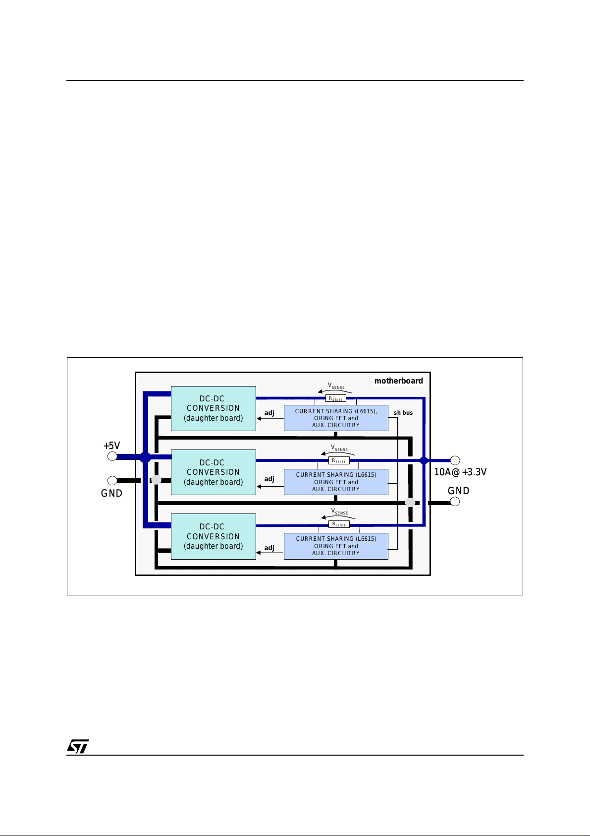
The system (fig. 2) is composed of:
2/11
Page 3
AN1696 APPLICATION NOTE
– three identical sections (daughter boards) able to perform DC-DC conversion starting from +5VDC;
each of them is designed to deliver 3.3V/5A to the load. They must be inserted in the motherboard;
– a motherboard whose input terminals will be connected to a +5V
minals to the load. This board can accommodate up to three DC-DC converters.
On the motherboard there is t he ci rcuitry necessary to perf orm current shari ng (L6615) and to isolat e a f ailed
section from the load; it is designed to be adaptable to all power supplies (whose rating are compatible with
L6615 absolute maximum ratings) having remote sense pi ns; i n f act onl y changing f ew components it c an be
rearranged for new specs.
external source and output ter-
DC
It is so possible to build a system to supply a
10A load at +3.3V in 2+1 redundant conf iguration.
That is,
whenever three sections are running, each of them supplies 3.33A, a value lower than its nominal capability.
If one of them is switched off, the sys tem is how ever able to supply the load and each section will car ry 5A.
The DC-DC conversion managem ent is entrusted to the L6910 [4].
It is possible to verify that disabling one section (through the relevant switch on the motherboard) does not cause
either overvoltage on the output or overcurrent in other sections.
At the same way, enabling one section (with other two already running) does not cause output voltage negative
drop or even short to ground and current sharing is established.
Figure 2. System overview
motherboard
motherboard
sh bus
sh bus
10A@+3.3V
10A@+3.3V
GND
GND
+5V
+5V
GND
GND
DC-DC
DC-DC
CONVERSION
CONVERSION
(daughter board)
(daughter board)
DC-DC
DC-DC
CONVERSION
CONVERSION
(daughter board)
(daughter board)
DC-DC
DC-DC
CONVERSION
CONVERSION
(daughter board)
(daughter board)
adj
adj
adj
adj
adj
adj
V
V
SENSE
SENSE
R
R
SENSE
SENSE
CURRENT SHARING (L6615),
CURRENT SHARING (L6615),
ORING FET an d
ORING FET an d
AUX. CIRCUITRY
AUX. CIRCUITRY
V
V
SENSE
SENSE
R
R
SENSE
SENSE
CURRENT SHARING (L6615)
CURRENT SHARING (L6615)
ORING FET an d
ORING FET an d
AUX. CIRCUITRY
AUX. CIRCUITRY
V
V
SENSE
SENSE
R
R
SENSE
SENSE
CURRENT SHARING (L6615)
CURRENT SHARING (L6615)
ORING FET an d
ORING FET an d
AUX. CIRCUITRY
AUX. CIRCUITRY
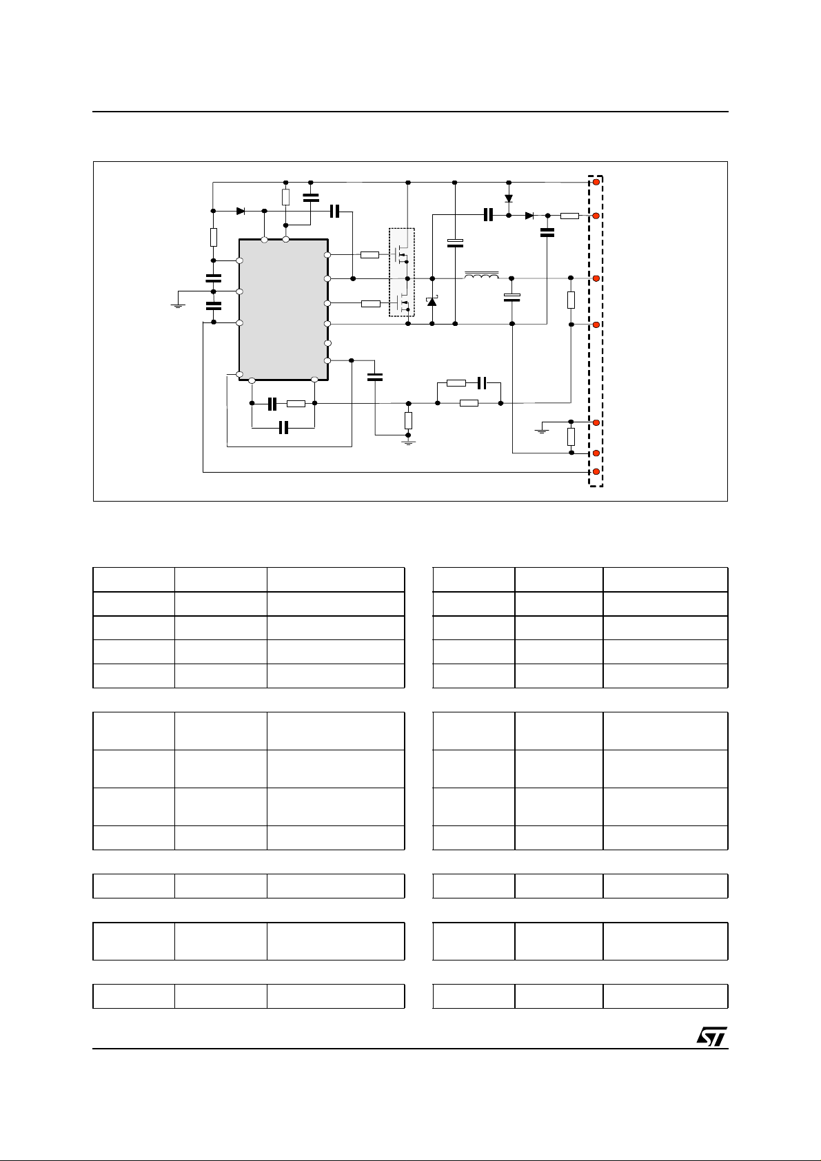
1.0 DAUGHTER BOARD
The L6910 controller drives a s ynchr onous step-down stage at 200KHz; t he internal reference is used for t he
regulation. The external power mosfet 's are included in one SO8 package to save space and increase power
density.
Fig. 3 shows the schematic of each daughter board and in table 1 the part list is indicated (for the description of
this section se e [4 ]).
3/11
Page 4
AN1696 APPLICATION NOTE
Figure 3. Daughter board schematic
R2
R2
D1
D1
BOOT
C4
C4
C3
C3
R1
R1
VCC
VCC
GND
GND
EAREF
EAREF
BOOT
15
15
7
7
SS
SS
4
4
8
8
12
12
L6910
L6910
5
5
COMP
COMP
C5
C5
OCSET
OCSET
3
3
R3
R3
C6
C6
11
11
10
10
14
14
13
13
6
6
9
9
VFB
VFB
C7
C7
1
1
C8
C8
UGATE
UGATE
PHASE
PHASE
LGATE
LGATE
PGND
PGND
PGOOD
PGOOD
VREF
VREF
R4
R4
R5
R5
C9
C9
Q1
Q1
R6
R6
D2
D2
R7
R7
C12
C12
C1–C2
C1–C2
L1
L1
C11
C11
C10
C10
R8
R8
D3
D3
D4
D4
C13
C13
R9
R9
R10
R10
R11
R11
VCC
VCC
PUMP
PUMP
OUT
OUT
+SOUT
+SOUT
SGND
SGND
PGND
PGND
SS
SS
Table 1. Part list board L6910
RESISTORS
R1, R9, R10 10 SMD 0805 R7 1K2 SMD 0805
R2 1K5 SMD 0805 R8 10K SMD 0805
R3 2K7 SMD 0805, 1% R9 82 SMD 0805
R4, R5 2.2 SMD 0805 R10 39 SMD 0805
R6 3K75 SMD 0805, 1% R11 680 SMD 0805
CAPACITORS
C1, C2 10µF (TOKIN)
C34Y5U1E106ZTE12
C3, C4,
100nF SMD0805, Ceramic C9, C10 10nF SMD0805, Ceramic
C8, C13
C5 47nF SMD0805, Ceramic C11 330 µF –
C6 N.C. SMD0805, Ceramic
INDUCTOR
L1 10µH T50-52B Core 12T
IC’s
C7, C12 1nF SMD0805, Ceramic
(POSCAP)
6.3V
6TPB330M
U1 L6910 (ST) SO16 NARROW Q1 STS8DNF3L
(ST) SO8
L
DIODES
D1, D3, D4 1N4148 SOT23 D2 STP130A SMA
4/11
Page 5

AN1696 APPLICATION NOTE
Besides the standard components necessary to perform DC-D C conversion, a charge pump (D3, D4, C12, C 13,
R11) has been added to provide a voltage high enough to bring the gate of the OR-ing FET (on the motherboard)
at least one threshold above V
with a lower R
and reducing mosfet conduction losses.
DS(ON)
This pump, running whenever PWM activity is present, pushes the gate of the OR-ing fet up to a voltage equal
to:
(1)
V
GATE MAX()
(where V
is the forward drop of the diodes) supplying a current equal to:
F
(2)
I
CHVINC12fSW
From the daughter board, besides input/output voltages and ground, other s ignals exit toward the motherboard:
– SOFT-START: the soft-start voltage is brought out and connected to a switch (that can short soft-start
to ground) allowing enable/disable of the relevant section;
– +SOUT and SGND are the sense t erminals for posi tive and negative load t erminals; they are c on-
nected to the relative power traces through two small resistors to avoid that any kind of open connection (or the sense pins left open) c ould caus e a lost of control.
OUT
(V
GATE
>3.3V+V
); moreover, increasing VGS voltage allows working
GS(TH)
2VIN2VF⋅–⋅=
⋅⋅=
2.0 MOTHERBOARD
The motherboard accommodates all the auxiliary circuitry necessary to load sharing, to manage start-up and to
enable/disable each of the three daughter boards; a LED indicates the disabled section.
Terminals are available to connect input DC voltage and load and three series of connectors allow inserting the
daughter boards.
In fig. 4 t he st ruct ure of one section of the motherboard is showed: repl ying t his structure other two times t he
entire board is obtained; table 2 reports the part list.
Figure 4. Motherboard schematic
C4
+ IN
+ IN
-IN
-IN
To other
To other
SECTIONS
SECTIONS
C4
1
1
8
Q1
R3
R3
LED
LED
R1
R1
C1
C1
R2
R2
R5
R5
8
8
D2
D2
D1
D1
1
1
R4
R4
Q1
R10
R8
R10
R8
R7
R7
7
7
(-)6
(-)6
(+)5
(+)5
U2
U2
C2
C2
3(+)42(-)
3(+)42(-)
SW1
SW1
R9
R9
VCC PGND
VCC PGND
C3
C3
SSOUT
SSOUT
R11
R11
R12
R12
PUMP
PUMP
+SOUT
+SOUT
PGND SGND
PGND SGND
C8
C8
C9
C9
8
2
2
7
7
U1
U1
3
3
6
6
4
4
5
5
D3
D3
R13
R13
Common
Common
SHARE BUS
SHARE BUS
C7
C7
R14
R14
C6
C6
R15
R15
C5
C5
C10
C10
JP1
JP1
SECTIONS
SECTIONS
To other
To other
+ OUT
+ OUT
- OUT
- OUT
5/11
Page 6

AN1696 APPLICATION NOTE
Table 2. Part list board L6615
RESISTORS
R1, R10 6K8 R5, R8 1K R13 82
R2 20K R7 330K R14 7K5
R3 2K R9 47K R15 100
R4 3K3 R11, R12 200
CAPACITORS
C1, C2, C4 100nF C5 1µF C8, C9, C10 open
C3 4.7µF C6, C7 10nF
IC’s
U1 L6615D (ST) SO8 U2 LM293 SO8
Q1 STS8DNF3LL (ST) SO8
DIODES
D1, D2, D3 1N4148 SOT23
To measure the current carried by each section, it is possible t o open the j umper JP1 (see schematic ) and to
place a ring for inserting a current probe.
2.1 OR- in g FE T a nd c urrent sensing
High side current sensing is implemented by reading the voltage drop across the R
of Q1 (during normal
DS(ON)
operation the FET is maintained on by the charge pump); the voltage at L6615 CGA pin of the section #N is
proportional to its output current, in particular [1]:
R
(1)
V
CGA
# N()I
OUT
# N()R
DS ON()
The first parameter to consider when selecting the OR-ing FET is its R
rent, it defines both the power dissipation and the dr op useful for cur rent sharing. Inc reasing R
14
---------⋅⋅=
R
12
because, for a given output cur-
DS(ON)
leads to
DS(ON)
a wide sense signal available but also means higher power dissipation.
In the motherboard Q1 is a STS8DNF3LL [5] having (for each MOS ):
0.017 (nom.)
DS(ON)
=
0.020Ω (max.)
@ ID=4A, VGS=10V, TCASE=25°C
DS(ON)
.
R
STS8DNF3LL contains two internal MOSFETs that are paralleled leading to halve the R
The design must be done considering worst case conditions to avoid share bus saturation: only two sections
running and maximum value for R
R
DS(ON)|@Tmax
= 0.015Ω
then the maximum drop will be 75mV and (1) leads to V
. Considering also the temperature variation, we have:
DS(ON)
CGA(MAX)
= V
SH(MAX)
of about 2.8V.
It can be useful to calculate the losses associated to the OR-ing FET and compare them with the losses in case
6/11
Page 7

AN1696 APPLICATION NOTE
of OR-ing diode (as a reference we consider the low drop Schottky diode STPS10L25D [6]).
Considering T
– OR-ing FET (STS8DNF3LL)
– OR-ing DIODE (STPS10L25 D)
and ID = 5A, we have:
max
P
DISSI D
P
DISS
2
0.22 I
R
DS ON()
D AVG()
0.375W=⋅=
0.013 I
2
DRMS()
1.425W=⋅+⋅=
Obviously in the case of the diode, also the sense resistor is needed: assuming the same 75mV drop, the total
dissipation will be 1.8W. We can estimate 1.4W saving, leading to about 8.5% efficiency rise.
2.2 Current sharing control
For each section one L6615 controller is associated with the few external components necessary to its operation.
Load sharing is achieved through a si ngle wire connection (share bus) between all t he paralleled modules,
whose voltage is proportional to the highest output current amongst all the active sections. In particular, being
unity the (internal) gain between CGA and SH pins, on the share bus there will be the highest of the values given
by (1).
In case of very noisy application, two capacitors (C8 and C9) allow filtering the L6615 current sense pins (#2
and #3).
The L6615 error amplifier is of transconductanc e type so a compensation network is required connec ted between L6615 pin #5 and ground; in this case an RC series network (C5-R15) determines a bandwidth of about
1KHz for the sharing loop.
The L6615 ADJ pin (pin#4) is connected to the daughter board: a current proportional to the output currents
unbalance is sunk from the feedback path of the relevant section.
The value of adjustment resistor (R13, between positive output terminal and ADJ pin) must be chosen in accordance with both the maximum current sink capability of pin ADJ and the output voltage tolerance.
If we consider V
= +3.3V with a tolerance of ±5%, the max imum spread between the master output voltage
OUT
and the slave one could be 330mV: this is the drop that the L6615 must be able to correct imposing a current
to flow through the adjustment resistor.
Its resistance value must be lower than the feedback divider (R6 and R8) to have no impact on the value of
regulated voltage.
The design of this resistor is a very simple process: it is enough to choose for the maximum adjustment current
a value lower than the maximum specified for L6615 (8mA, worst case) and verify that this does not cause the
saturation of the L6615 internal BJT (see fig. 5) under steady state condition.
In this case :
adj. current: I
min adj. resistor:
ADJ(max)
R
= 8mA
ADJ min()
∆V
OUT MAX()
----------------------------------
I
ADJ
330mA
------------------- 41.25Ω===
8mA
In fact this resistance value is obtained considering the parallel of R13 (motherboard) and R9 (daughter board),
each of them equal to 82
Ω
.
7/11
Page 8

AN1696 APPLICATION NOTE
Figure 5. Adj ust m ent network
V
= +3.3V
V
= +3.3V
OUT
OUT
R
R
13
13
C
C
10
L6910
L6910
V
V
DAUGTHERBOARD
DAUGTHERBOARD
10
R
R
FB
FB
R
R
8
7
7
8
R
R
6
6
2.3 Gate driver of OR-ing FET
The OR-ing FET gate is driven by the output of a comparator (one section of an LM293, standard double comparator) sensing the voltage upstream (source) and downs tream (drain) the OR-ing FET (see fig. 6). This turnsoff the transistor whenever a current tries flowing from the load towards the output stage of a daughter board.
MOTHERBOARD
MOTHERBOARD
I
I
ADJ
ADJ
ADJ
ADJ
R
R
A
A
+
+
-
-
L6615
L6615
Whenever one section is enabled with the two others already runni ng (hot pl ug), its output capacitor is completely discharged: to avoid a negative drop on the load v oltage, t he gat e of t he FET i s kept l ow until V
reaches a value very close to V
charging output capacitor (V
V
COUT()ON–
C(OUT
(this can be set defining t he r at io between R5 and R7). The PWM starts
LOAD
) increases) and, only when:
V
1
------- -+
⋅ V
REF
R7
R5
LOAD
R8
----------------------
⋅⋅==
R8 R9+
1
R5
------- -⋅
R7
C(OUT)
the FET is turned on.
Moreover the load must be isolated from a failed section; for example in case of a short circuit on the low side
power MOS of one section, then a current will tend to flow in reverse direction through the corresponding ORing FET.
Figure 6. OR-ing FET management
DAUG HTERBOARD MOTHE RBOARD
DAUG HTERBOARD MOTHE RBOARD
R5
R5
V
V
V
C(OUT)
C(OUT)
PUMP
PUMP
CHARGE
CHARGE
R11
R11
V
V
PUMP
PUMP
V
GATE
GATE
R7
R7
-
-
+
+
V
V
PS+
PS+
R8
R8
V
V
R9
R9
V
V
C(OUT)
C(OUT)
SECTIONS
SECTIONS
L
L
L
O
O
O
V
V
LOAD
LOAD
A
A
A
D
D
D
REF
REF
C2
C2
ALREADY
ALREADY
RUNNING
RUNNING
V
V
PS+
PS+
V
V
GATE
GATE
V
V
C(OUT)-O NVC(OUT)-OFF
C(OUT)-O NVC(OUT)-OFF
∆V
∆V
HYST
HYST
V
V
LOAD
LOAD
V
V
REF
REF
V
V
PUMP
PUMP
8/11
Page 9

AN1696 APPLICATION NOTE
3
For a short time (before overcurrent/undervoltage protections are triggered), the unbroken sections are able to
deliver such high current maintaining the load voltage in the right range.
This in turn ca u ses V
V
C(OUT)-OFF
.
It is possible to obtain the value of the current necessary to push V
to be lower than V
C(OUT)
I
REV
---------------------- - V
R
and the OR-ing FET will be turned off whenever V
LOAD
1
⋅=
DS ON()
LOAD
R9
1
----------------------
R8 R9+
at V
C(OUT)
R5
1
------- -+
⋅–
R7
R5
------- -⋅+⋅
R7
:
C(OUT)-OFF
V
PUMP
C(OUT)
=
3.0 DEMO-BOARD BEHAVIOUR
The aim of this demo-board is mainl y to show the operat ion of current s haring section, drawing the attention
also to the management of the OR-ing FET. For this reason no protection have been introduced to prevent inrush current: it is not possible to actually insert or remove a daughter board during normal operating, nevertheless it is recommended to simulate a fault by enabling/disabling one section through the switch SW1 (it shorts
to GND th e so ft- sta r t p in).
Once all the daughter board are inserted (wi th the switches on the "ON" position), the system is r eady to be
powered-up.
Measuring the three output currents and varying the load continuously, it is possible to see the load share accuracy (fig. 7); obviously, at light load, the accuracy is not so high because is higher the weight of both the mismatches between relevant components and the noise is hi gher. At ful l load (10A) the maximum error i s lower
than 2.5%.
Fig. 8 shows the behaviour of the system whenever a fault condition appears on section 1 when the three sections are operating supplying a total load of 10A (each of them carries about 3.3A); in particular it is simulated
a short of the low side FET of the synchronous rectifier section 1.
If no OR-ing element were implemented, this could cause a short circuit condition on the other two sections (UV
and/or overcurrent protection could be activated): here the gate driver circuit opens the OR-ing FET preventing
current flow from the load to the output of section 1 and the output voltage experiences only a very small drop.
The currents of section 2 and 3 grow up to 5A.
Figure 7. Load share accuracy Figure 8. Fault on one section
30
25
20
15
10
5
0
-5
-10
-15
Load share accuracy [%]
-20
-25
-30
I
OUT2
10 20 30 40 50 60 70 80 90 100
I
OUT
I
OUT1
Output current [%]
9/11
Page 10

AN1696 APPLICATION NOTE
REFERENCES
[1] "L6615 High/low side load share controller" (Datasheet)
[2] V. J. Thouttevelil, C. G . Ver ghes e, "Analysis and cont ro l Des ign of Paralleled DC/DC Conv er ters with
Current Sharing", IEEE Trans ac t ion on P ower Ele ctr onic s, Vol. 13, N. 4, July 1998, pp. 635-644.
[3] J. Rajagopalan, K. Xing, Y. Guo, F.C. Lee, B. Manners, "Modeling and Dynamic Analysis of Paralleled
DC-DC Converters with Master-Slave Current-Sharing control", IEEE Applied Power Electronics
Conf. Rec. 1996, pp 678-684.
[4] "L6910 - Adjustable step down controller with synchronous rec tific ation" (Datasheet)
[5] "STS8DNF3LL, DUAL N-CHANNEL 30V - 0.017 OHM - 8A SO-8 LOW GATE CHARGE STRIPFET II
POWER MOSFET" (Datasheet)
[6] "STPS10L25D, LOW DROP POWER SCHOTT KY RECTI FI ER " (Dat as heet)
APPENDIX
LAYOUT
Figure 9. Daughter board layout and connectors configu rati on
10/11
PUMP
PUMP
PUMPSSSS
PUMPSSSS
J2 J3 J1
J2 J3 J1
-SOUT
-SOUT
-SOUT
-SOUT
GND
GND
GND
GND
GND
GND
GND
GND
VCC
VCC
VCC
VCC
VCC
VCC
VCC
VCC
+SOUT
+SOUT
+SOUT
+SOUT
OUT
OUT
OUT
OUT
OUT
OUT
OUT
OUT
GND
GND
GND
GND
GND
GND
GND
GND
Page 11

Figure 10. Motherboard layout
AN1696 APPLICATION NOTE
Information furnished is believed to be accurate and reliable. However, STMicroelectronics assumes no responsibility for the consequences
of use of such information nor for any infringement of patents or other rights of third parties which may result from its use. No license is granted
by implic ation or otherwise under any patent or patent r i ght s of STMi croelectr oni cs. Specifications menti oned in thi s publicati on are subj ect
to change without notice. This publication supersedes and replaces all information previously supplied. STMicroelectronics products are not
authorized for use as cri tical components in li f e support dev i ces or systems without express writ t en approval of STMicroel ectronics.
The ST logo is a registered trademark of STMicroelectronics
2003 STMicroelectronics - All Ri ghts Rese rved
Austra lia - Brazil - Canada - Ch i na - F i nl and - France - Germany - Hong Kong - India - Israel - Italy - Japan -Malay si a - Malta - Morocco -
Singap ore - Spain - Sw eden - Switzerland - Uni ted Kingdom - United St ates.
STMicroelectronics GROUP OF COMPANIES
http://www.s t. com
11/11
 Loading...