

Page 1
AN1695
APPLICATION NOTE
TSM108 EVALUATION BOARD
12V to 6V DC/DC CONVERTER
by Anthony BOIMOND
1 - Introduction
The TSM108 is a step down controller that features constant voltage and constant current regulation. It
can drive either a P-channel Mosfet or a PNP bipolar transistor. The principle of operation of the TSM108
is widely described in the application note attached to the datasheet. The goal of t his document is to
describe the TSM108 Evaluation Board.
The Evaluation Board was designed to allow different converter configurations. Several options for power
semiconductor footprints are avai lable on the PCB in order to make it adaptable to a wide range of
converter output power. In a first step, this applicati on note will des cribe th e typical appli cation . Then the
various options available on the Evaluation Board PCB will be explained.
2 - TSM108 typical application
2.1 Description
The TSM108 is especially suited for cigarette lighter accessories. The typical application described in this
note is a battery charger with the following characteristics:
Input voltage: Vin = 12V
Output voltage: Vout = 6V
Maximum output current: Iout = 800mA
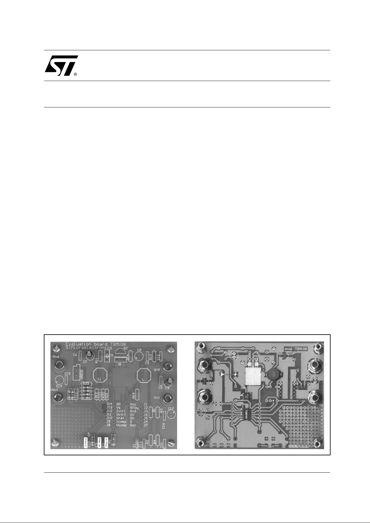
A picture of the Evaluation Board in the typical application configuration is shown on Figure 1. The related
schematic is described on Figure 2.
Figure 1 : TSM108 Evaluation Board
January 2003
1/5
Page 2
AN1695 - APPLICATION NOTE
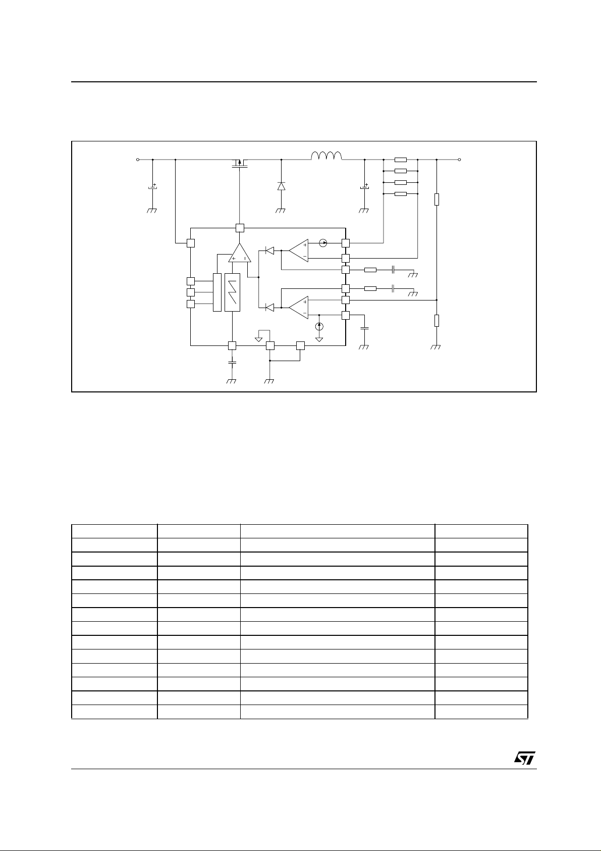
Figure 2 : Typical application schematic
Vin Vout
C4 C7
U1
VCC
1
!STBY
2
UV
4
OV
5
TSM108
Q4-B
L1
Q4-A
14
GD
UV/OV/!STBY
OSC
7
C1
GND
3
200mV
VS
13
ICTRL
12
ICOMP
VCOMP
VCTRL
VREF
2,52V
G
6
R7
9
R6
8
11
10
C10
R8
R17
R18
R19
R9
C3
C2
R10
The list of components used in the typical application board is shown in the bill of material here below. All
other components are not mounted. Passive components like capacitors and resistors used in this
Evaluation Board a re through-hole components to be more easily changed by the user. Of course, in
real-life application, surface-mounted devices will be used and the whole application can fit into a very
small PCB area.
Table 3 : Bill of mater ial
Reference Value Description Manufacturer
U1 TSM108ID PWM controller STMicroelectronics
Q4 STS3DPFS30 Mosfet + diode STMicroelectronics
L1 P0250.154T 150µH - buck main inductor Pulse
L short circuit filtering inductor
C1 220pF oscillator capacitor
C2-C3 22nF compensation capacitors
C4-C7 47µF-25V buck input and output capacitors Rubycon ZL
C10 100nF voltage reference bias capacitor
R8-R17-R18-R19 1Ω shunt resistor
R6-R7 22kΩ-10% compensation resistors
R9 15kΩ-1% divider bridge upper resistor
R10 11kΩ-1% divider bridge lower resistor
R16-R22 short circuit
2/5
Page 3

AN1695 - APPLICAT ION NOTE
2.2 Performances
As explained in the datasheet, the step-down converter using TSM108 can feature an accurate
constant-voltage and constant-current regulation. The V/I output characteristics of the DC/DC converter is
shown in Figure 4. Input voltage wa s set at 12V during this test. As explained in introducti on, voltage
regulation is set to 6V and current regulation is set to 800mA. At output voltage lower than 1V, the
foldback can be observed in the current regulation.
Figure 4 : Output voltage versus output current characteristics
7
6
5
4
Vout (V)
3
2
1
0
0 100 200 300 400 500 600 700 800 900
Iout (mA)
The efficiency of the DC/DC converter was measured in different conditions, as shown in Figure 5.
On the left chart, the influence of output power (Pout) over efficiency is studied. It should be noted that
during this test, the converter was operating in constant-voltage mode, therefore with Vout=6V and
Iout<800mA. Input voltage V in was equal to 12V during the test. The efficiency appears to be always
between 84% and 90%.
On the right chart, the influence of input voltage (Vin) over efficiency is studied. The converter was
operating in constant-voltage mode and the output power was constant equal to 4W during the test. With
the input voltage varying from 7 V up to 25V, the converter efficiency app ears to be between 84% and
90%.
Figure 5 : Efficiency of the DC/DC converter versus output power and input voltage
Efficiency vs. Output Power @ Vout=6V Vin=12V
94%
92%
90%
88%
86%
84%
82%
0 1000 2000 3000 4000
Pout (mW)
Efficiency vs. Input Voltage @ Vout=6V Pout=4,0W
94%
92%
90%
88%
86%
84%
82%
510152025
Vin (V)
3/5
Page 4

AN1695 - APPLICATION NOTE
L
ICOMP
VCOMP
VCTRL
3 - Evaluation board description
The TSM108 ev aluation b oard is easily a daptable to a wide rang e of output power. Several options are
available on the board for the power semiconductor packages. Figure 4 shows the electrical connections
of all the components available on the Evaluation Board printed circuit board.
Figure 6 : Evaluation Board complete schematic
Q2
R15
R23
R19
R12
R18
R17
R8
R16
VRES1 C15
C12
R13
Vin Vout
C4 C14
C5 R1R2R3R4C16 C17 C9 C8 R22
L
R14
Q1
Q3
Q4-B
R11
D1
Q4-A
L1
C6 C7
U1
VCC
1
!STBY
2
UV
4
OV
5
C11C13
C1
OSC
7
14
GD
TSM108
GND
3
VS
13
ICTR
12
11
R7R6C3
9
8
G
VREF
6
10
C2
C10
R20
Figure 7 : Evaluation board top layer silk screen and bottom layer overview
R21
R9
R10
4/5
Page 5

AN1695 - APPLICAT ION NOTE
The typical application described previously uses a power MOSFET and a schottky diode integrated in the
same SO8 package, but several options for power semiconduct or footprints are available on the PCB in
order to make it adaptable to a wide range of converter output power. The power switch can be replaced
by a MOSFET in TO220 or D2PAK package, but also by a bipolar in TO92 package. The diode can be
replaced by an axial or TO220 package. The various options available on the Evaluation Board are
presented in Table 8 here below.
Table 8 : Power semiconductors options available on the Evaluation Board
Component Designator Package Pinout (topview)
Power Switch
(P-Mosfet)
Q1 TO220
Q3 D2PAK
Q4-B half SO8
DGS
GS
D
1
2
3
4 5
8
7
6
Power Switch
Q2 TO92
(PNP bipolar )
B
CE
Power Diode D1 TO220 or axial
KA
Q4-A half SO8
1
2
3
4 5
Information furnished is bel ieved to be accurate and reliable. However, STMicroe lectronics assumes no responsibility for the
consequences of use of such information nor for any infringement of patents or other rights of third parties which may result from
its use. No li cense is granted by imp lication or otherwise under a ny patent or patent rig hts of STMicroelectronics. Spec ific at ions
mentioned in this publication ar e subject to change without notice. This publication supersedes and replaces all information
previously supplied. S TMicroelectronics products are not authorized for use as critica l components in life suppo rt devices or
systems without express written approval of STMicroelectronics.
© The ST logo is a registered trademark of STMicroelectronics
© 2003 STM icroelectronics - Printed in Ital y - All Rights Reserved
STMicr o el ectronics GROUP OF COMPANIES
Australi a - Brazil - Chi na - Finland - F rance - Germany - Hong Kon g - I ndia - Italy - Japan - Malay sia - Malta - Morocco
Singapo re - Spain - Sweden - Switzerland - Uni ted Kingdom
© http://www.st.com
8
7
6
5/5
 Loading...