

Page 1
AN1690
Application note
Fail-safe biasing for ST485EB
Introduction
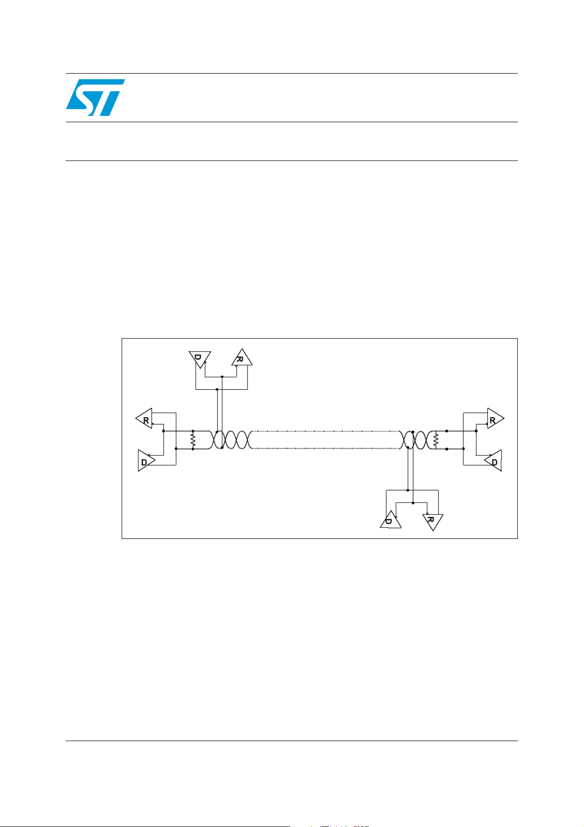
ST485EB is an RS-485 based interface designed for multipoint differential transmission on a
single twisted pair cable. It allows half duplex bi-directional transmission, long cable lengths
and high data rates.
Typical applications include LANs, industrial (PLC devices), automotive and computer
interfaces.
System evolution in the data communication field has lead to the development of faster
devices with lower data bit error rates. The ST485EB meets all these requirements. Figure 1
shows a typical multipoint bus configuration.
Figure 1. Typical RS-485 line
October 2007 Rev 2 1/15
www.st.com
Page 2

Contents AN1690
Contents
1 Overview . . . . . . . . . . . . . . . . . . . . . . . . . . . . . . . . . . . . . . . . . . . . . . . . . . 4
2 Bus states . . . . . . . . . . . . . . . . . . . . . . . . . . . . . . . . . . . . . . . . . . . . . . . . . 4
3 Data transmission protocol . . . . . . . . . . . . . . . . . . . . . . . . . . . . . . . . . . . 5
4 Internal fail-safe and bus termination . . . . . . . . . . . . . . . . . . . . . . . . . . . 6
5 DC terminated fail-safe resistor value calculations . . . . . . . . . . . . . . . . 7
5.1 Example calculation . . . . . . . . . . . . . . . . . . . . . . . . . . . . . . . . . . . . . . . . . . 7
6 AC terminated fail-safe resistor . . . . . . . . . . . . . . . . . . . . . . . . . . . . . . . . 9
7 Fail-safe in multipoint transmission buses . . . . . . . . . . . . . . . . . . . . . . 10
8 Fail-safe circuit comparisons with ST485EB . . . . . . . . . . . . . . . . . . . . 11
9 Conclusion . . . . . . . . . . . . . . . . . . . . . . . . . . . . . . . . . . . . . . . . . . . . . . . . 14
10 Revision history . . . . . . . . . . . . . . . . . . . . . . . . . . . . . . . . . . . . . . . . . . . 14
2/15
Page 3

AN1690 List of figures
List of figures
Figure 1. Typical RS-485 line. . . . . . . . . . . . . . . . . . . . . . . . . . . . . . . . . . . . . . . . . . . . . . . . . . . . . . . . 1
Figure 2. Differential plot for driver outputs . . . . . . . . . . . . . . . . . . . . . . . . . . . . . . . . . . . . . . . . . . . . . 4
Figure 3. Asynchronous UART sequence format . . . . . . . . . . . . . . . . . . . . . . . . . . . . . . . . . . . . . . . . 5
Figure 4. Terminated line (on both sides) . . . . . . . . . . . . . . . . . . . . . . . . . . . . . . . . . . . . . . . . . . . . . . 6
Figure 5. Open terminated line (end side only) . . . . . . . . . . . . . . . . . . . . . . . . . . . . . . . . . . . . . . . . . . 6
Figure 6. Unterminated or open line . . . . . . . . . . . . . . . . . . . . . . . . . . . . . . . . . . . . . . . . . . . . . . . . . . 6
Figure 7. External fail-safe and line DC termination resistors . . . . . . . . . . . . . . . . . . . . . . . . . . . . . . . 7
Figure 8. AC termination with external fail-safe . . . . . . . . . . . . . . . . . . . . . . . . . . . . . . . . . . . . . . . . . . 9
Figure 9. Multipoint transmission line with ST485EB. . . . . . . . . . . . . . . . . . . . . . . . . . . . . . . . . . . . . 10
Figure 10. Equivalent test circuit for a fully loaded network. . . . . . . . . . . . . . . . . . . . . . . . . . . . . . . . . 11
Figure 11. DC fail-safe characteristics . . . . . . . . . . . . . . . . . . . . . . . . . . . . . . . . . . . . . . . . . . . . . . . . . 12
Figure 12. Fail-safe DC termination - eye pattern and test circuit . . . . . . . . . . . . . . . . . . . . . . . . . . . . 13
Figure 13. Fail-safe AC termination - eye pattern and test circuit . . . . . . . . . . . . . . . . . . . . . . . . . . . . 13
3/15
Page 4
Overview AN1690
1 Overview
In a point-to-point configuration (such as the RS-422 standard) the driver is normally always
enabled.
The bus can remain only in the HIGH or LOW state (the bus is always biased). In a
multipoint application, when more than one driver is physically connected to the bus and
only one driver at a time is enabled during data transmission, all the drivers can be disabled
when there is no data to send. In this case there is no bus biasing (undefined state). Failsafe biasing solves this problem providing the bus with a proper known state. This
application note describes the topic of fail-safe biasing.
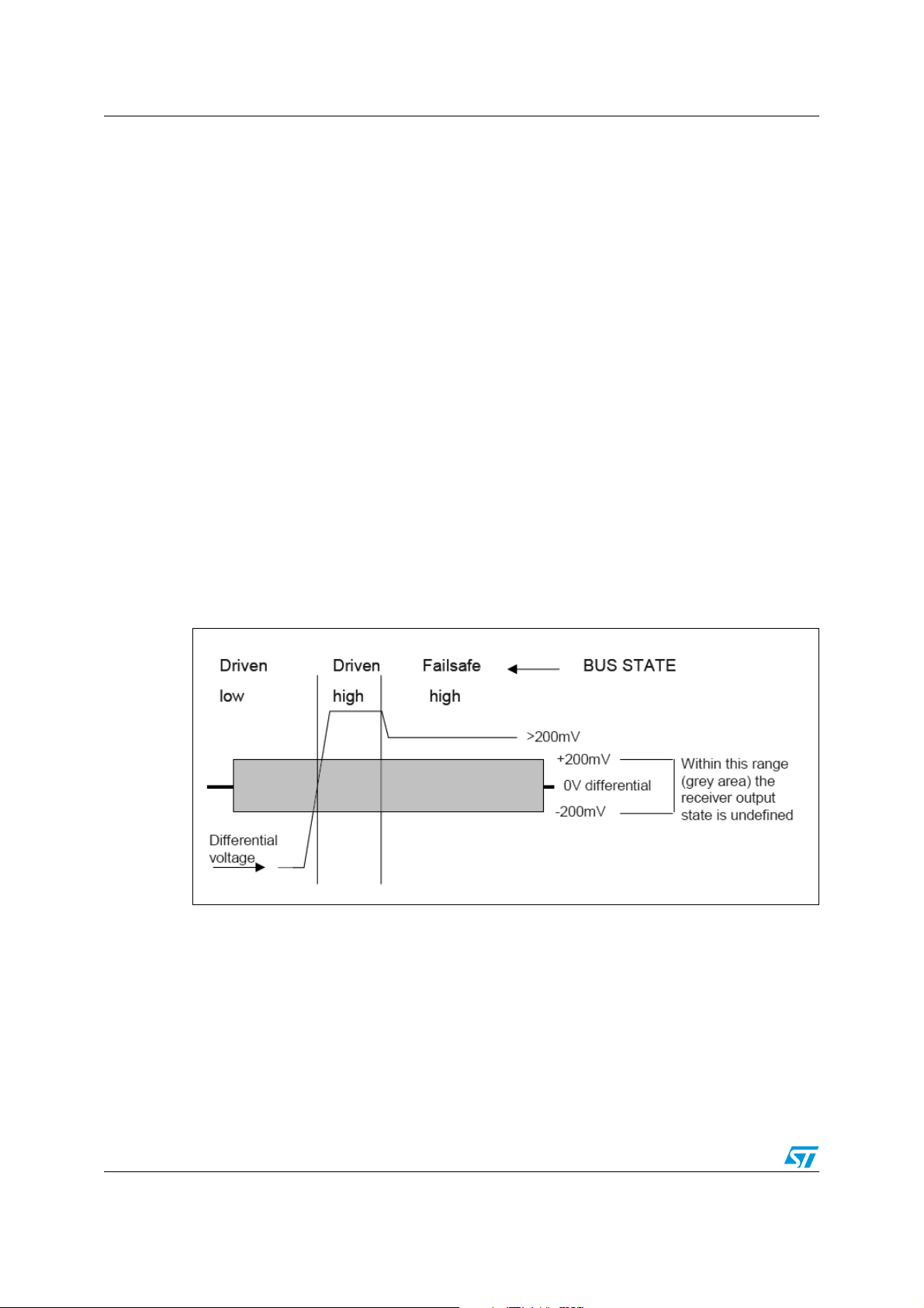
2 Bus states
When a bus is driven by an active driver, it can be in one of two states, either high or low. It
can also be kept in one of these states by external pull-up resistors that provide the
necessary voltage to get a known bus state. The undefined state in RS-485 standard buses
occurs every time the differential voltage is less than +/-200 mV. In Figure 2 the bus is driven
from low to high and is then disabled. The bus, however, remains high due to external failsafe biasing.
Figure 2. Differential plot for driver outputs
4/15
Page 5
AN1690 Data transmission protocol
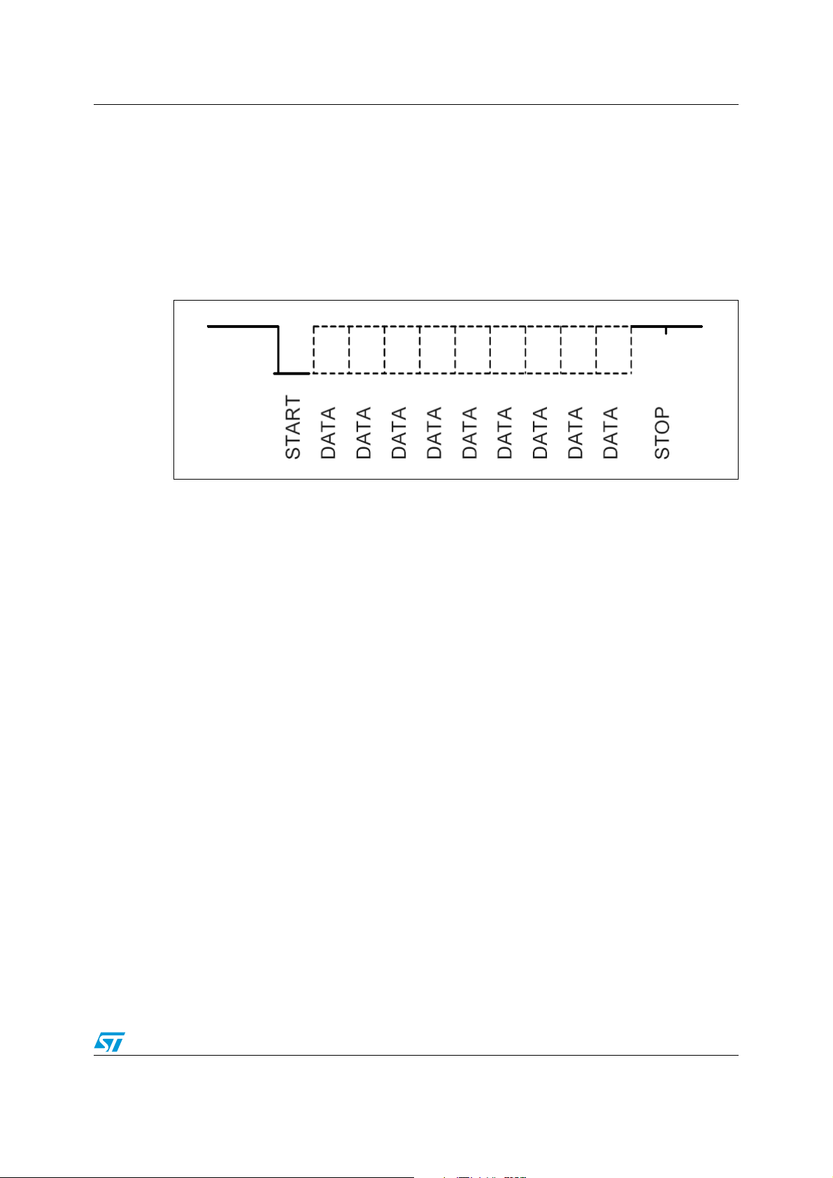
3 Data transmission protocol
One of the most well known formats for low speed data transmission is the UART timing
format. It is an asynchronous protocol, typically composed of 12 bits. The timing sequence
starts with a transition from high to low. Next there are 9 data bits (8 data bits plus a parity
bit). Finally, the line remains high for one or two bits, which represents the end of the
character.
Figure 3. Asynchronous UART sequence format
In a multipoint application, when no more data has to be sent, the line should remain high
until the next start bit. Since the active driver is disabled, and all other drivers are off, this is
not easy to achieve.
One way to solve this problem is the use of an alternate protocol (software solution). The
other way is to use fail-safe biasing (hardware solution).
5/15
Page 6

Internal fail-safe and bus termination AN1690
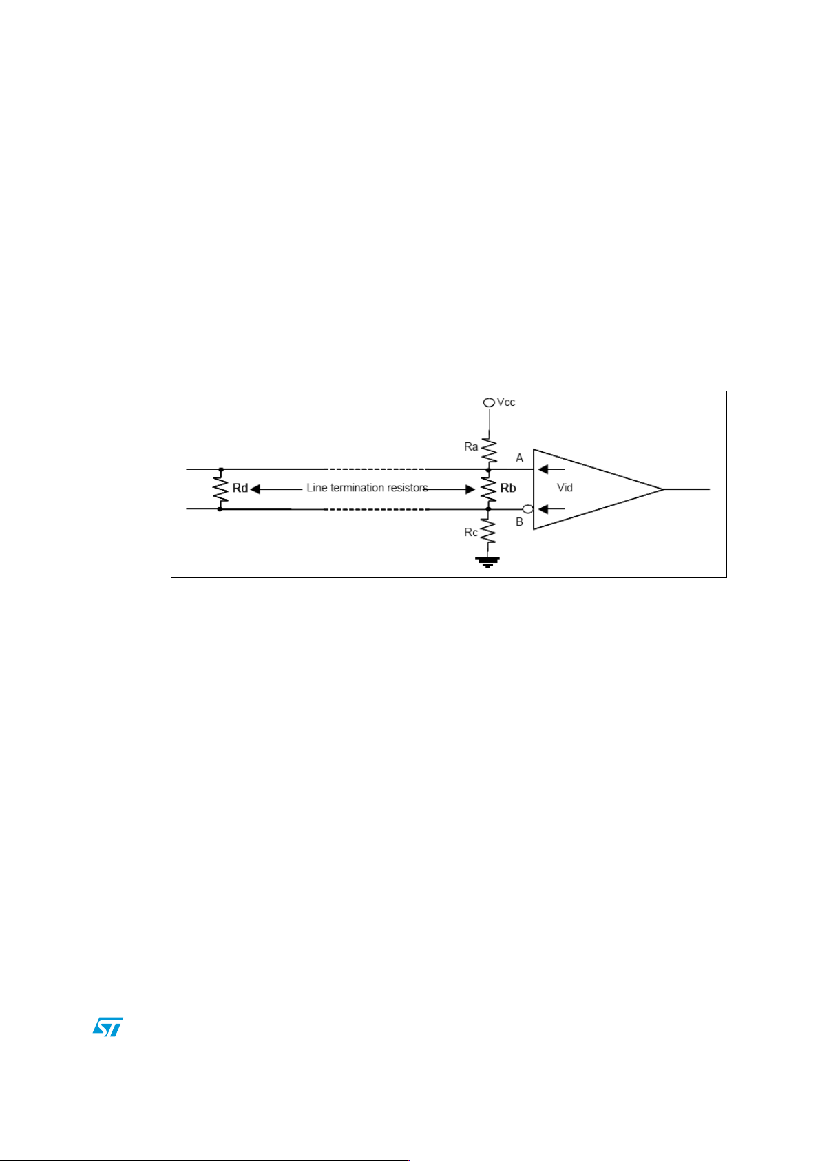
4 Internal fail-safe and bus termination
Transceiver manufacturers avoid external biasing resistors by providing internal pull-up
resistors at the receiver inputs, which is effective for detecting open circuits or for those
applications where termination resistors are not needed. The line termination resistors
(typically 54~120 Ω for a twisted pair cable) load the line avoiding the need for internal pull-
up resistors to define the receiver output. Figure 4, Figure 5, and Figure 6 show differential
voltage levels for different line conditions for the ST485EB receiver interface.
Note: There is no driver leading the line.
Figure 4. Terminated line (on both sides)
Figure 5. Open terminated line (end side only)
Figure 6. Unterminated or open line
6/15
Page 7
AN1690 DC terminated fail-safe resistor value calculations
5 DC terminated fail-safe resistor value calculations
The external resistors are selected so that they provide at least a 200 mV bias across the
line, without excessively loading the active driver. In addition, some other conditions should
be met:
● The pull-up (Ra) and pull-down (Rc) resistors should be of equal value in order to load
the driver outputs symmetrically.
● Termination resistor (Rd) should match the characteristic impedance (Zo) of the line
cable, in order to avoid signal reflections.
● At the other end of the cable, the equivalent resistance of Ra, Rb, and Rc should also
match the characteristic impedance of the line. In the following Figure 7, the equivalent
resistance is Rb II (Ra+Rc), which means Rb must be greater than Zo and Rd.
Figure 7. External fail-safe and line DC termination resistors
The fail-safe bias Vid is the voltage drop across the line. Therefore, the fail-safe bias is
simply a voltage divider between Rb II Rd, Ra and Rc. Note that this formula neglects cable
resistance, and that Rb is parallel to Rd (Rb II Rd).
The choice of resistors must take into account other factors such as power supply voltage
tolerance and resistor tolerance, so that under worst case conditions, Vid is greater than
200 mV.
5.1 Example calculation
For this example, based on Figure 7, we assume that the cable has a characteristic
impedance Zo=120 Ω and that the power supply voltage Vcc is 5 V. We also assume that Rb
and Rd are equal and their value matches Zo (Rb=Rd=Zo=120 Ω).
● Calculate the equivalent resistance of Rb II Rd. Rt = 120 II 120 = 60 Ω.
● Calculate Ra and Rc for a Vid = 200 mV.
– Vid = Vcc (Rt/(Rt+Ra+Rc)). Solving for Ra+Rc
– Ra+Rc = ((Vcc)Rt/Vid)-Rt. Ra+Rc = ((5 V)60 Ω/0.2 V)-60 Ω = 1440 Ω.
– Ra = Rc = 720 Ω
● Recalculate the equivalent termination resistance at the end of the cable.
Req = Rb II (Ra+Rc). Rb = 120 II (720+720) = 110 Ω. This value is close (<10%) to the
characteristic impedance Zo. However Req could be matched to Zo by setting the
following equation:
7/15
Page 8

DC terminated fail-safe resistor value calculations AN1690
Equation 1
Zo Rb Ra Rc+()
||
=
Then
Equation 2
Rb 131 Ω=
● The calculated values for Ra and Rc could be slightly decreased to provide a
Vid >200 mV, and to meet the worst case power supply and resistor tolerance
conditions. Then Ra and Rc could be 500 Ω. However the value of Ra and Rc should
not be reduced too low in order to minimize the driver loading when the driver is active.
An active driver is required to create a minimum of 1.5 V across the cable termination.
The use of low resistance pull resistors makes this voltage more difficult to meet.
8/15
Page 9

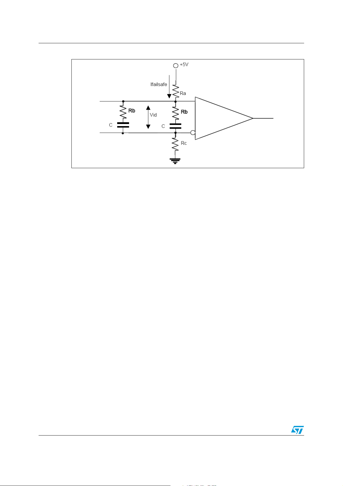
AN1690 AC terminated fail-safe resistor
6 AC terminated fail-safe resistor
The DC termination (with and without fail-safe biasing) increases power consumption due to
the current flow through the termination resistors. In order to reduce the current absorbtion,
the fail-safe network could be modified as shown in Figure 8.
Figure 8. AC termination with external fail-safe
The RC termination blocks DC current. The value of Ra and Rc can be increased, but not so
much that noise immunity is made worse.
Although Rb always equals the cable’s characteristic impedance (Zo), the choice of C
requires some judgement. Large C values provide good terminations by allowing any signal
to see an Rb that matches Zo, but large values also increase the driver’s peak output current
and the time constant RC, therefore decreasing signal quality.
9/15
Page 10

Fail-safe in multipoint transmission buses AN1690
7 Fail-safe in multipoint transmission buses
As discussed in the example of the calculation for fail-safe resistors, when calculating their
values, the following conditions must be satisfied:
● The driver must be able to develop a differential output voltage Vod >=1.5 V
The excessively low resistance of the pull resistors could affect the driver differential output
voltage. In a multipoint application, where up to 32 transceivers could be connected in
parallel to the transmission line (Figure 9), the differential output voltage drops, due to the
equivalent input impedance of all the receivers connected. A minimum input impedance of
12 kΩ for each receiver is required, so in the worst case of a fully loaded network (32 unit
loads) the equivalent resistance seen by the active driver is (12 kΩ / 32) = 375 Ω.
Figure 9. Multipoint transmission line with ST485EB
This value should be reduced in order to take into account that there are 31 drivers in a high
impedance state, each with a leakage current. However in the ST485EB device this current
is less than 10 µA, so its effect can be neglected. With regard to the ground shift, the
previous schematic can be modelled as shown in Figure 10, in order to verify the driver
output voltage capability.
10/15
Page 11
AN1690 Fail-safe circuit comparisons with ST485EB
Figure 10. Equivalent test circuit for a fully loaded network
Vcc1
Vcc1
ST485
ST485
Driver
Driver
EB
Vod
Vod
Ra
Ra
Rc
Rc
Rb
Rb
32 unit loads
32 unit loads
375
375
375
375
Vcm= -7 to
Vcm= -7 to
+7V
+7V
Vcc2
Vcc2
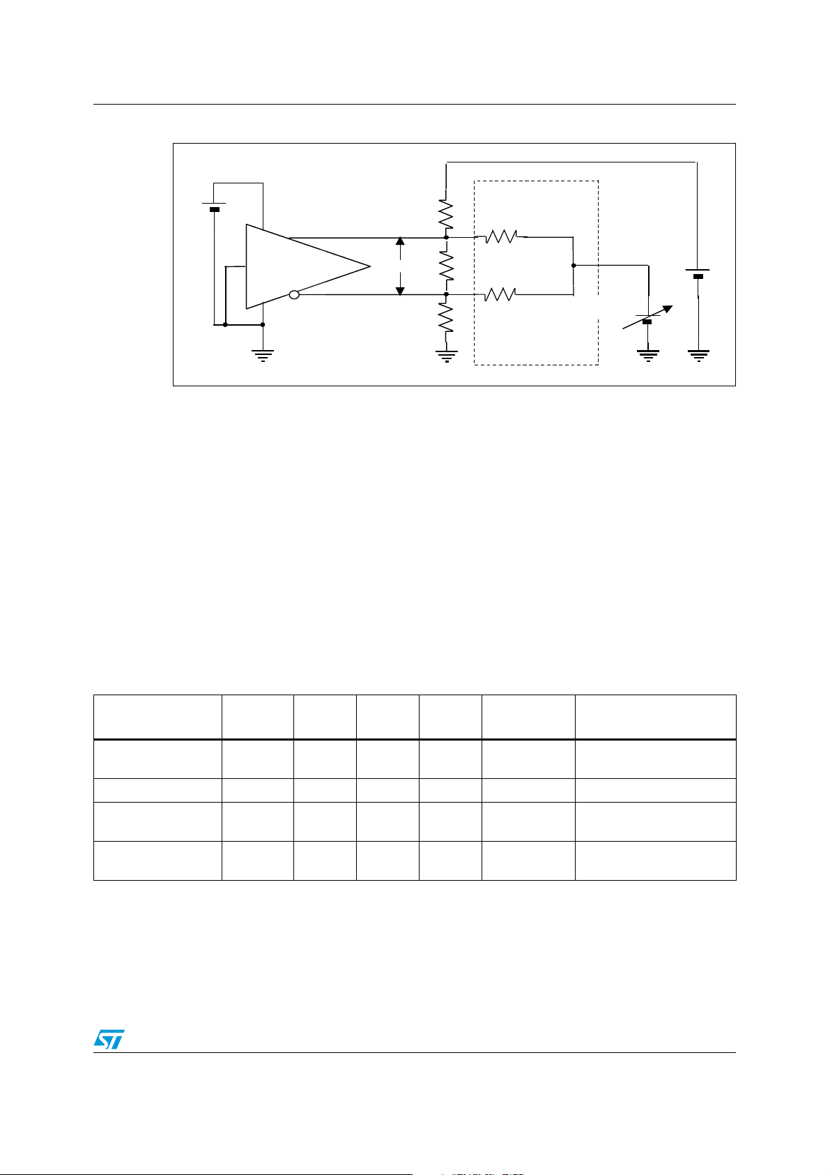
This test was performed on the ST485EB driver. The resistor values were:
● Ra = Rc = 500 Ω
● Rb = 60 Ω
With the common mode voltage Vcm varied from -7 to +7 V, the device meets the 1.5 V
minimum differential voltage (Vod).
8 Fail-safe circuit comparisons with ST485EB
The following measurements were performed with two ST485EB devices connected in
point-to-point configuration across a twisted pair cable of 1 m length. Tab l e 1 summarizes
the DC characteristics with different termination circuits.
Table 1. DC fail-safe characteristics
Schematic Ra=Rc (Ω)Rb (Ω) C (nF) Vid (mV)
No termination - - - 1430 -
DC termination - 120 - 1.45 - Undefined
Fail-safe DC
termination
Fail-safe AC
termination
500 120 - 280 4.72 Fixed high
22 kΩ 120 100 4040 0.0316 Fixed high
Note: Vcc=5 V
Fail-safe
current (mA)
Receiver output state
Fixed high (internal failsafe)
11/15
Page 12
Fail-safe circuit comparisons with ST485EB AN1690
Figure 11. DC fail-safe characteristics
Another test was performed to verify the behavior of the different termination circuits when
an AC signal is present on the line. Figure 12 and Figure 13 show the eye patterns of the
signals driven respectively at the end of a 100 m cable and on the receiver output. The
driver was led by means of a PRBS (pseudorandom bit signalling) generator with 5 Mbit/s
data rate.
12/15
Page 13

AN1690 Fail-safe circuit comparisons with ST485EB
C
Rc
Ra
Rb
C
Rb
PRBS
GENERATOR
CH1
differen tial
probe
CH3
probe
100m
cable
Receiver
Input
Receiver
Output
C
Rc
Ra
Rb
C
Rb
PRBS
GENERATOR
CH1
differen tial
probe
CH3
probe
100m
cable
C
Rc
Ra
RbRb
CRbC
RbRb
PRBS
GENERATOR
CH1
differen tial
probe
CH3
probe
100m
cable
Receiver
Input
Receiver
Output
Receiver
Input
Receiver
Output
Figure 12. Fail-safe DC termination - eye pattern and test circuit
Receiver
Receiver
Receiver
Input
Input
Input
Receiver
Receiver
Receiver
Output
Output
Output
PRBS
PRBS
PRBS
GENERATOR
GENERATOR
GENERATOR
120
120
120120120
100 Cable
100 Cable
100 Cable
CH1
CH1
CH1
differential
differential
differential
probe
probe
probe
500
500
500
130
130
130
500
500
500
CH3
CH3
CH3
probe
probe
probe
Figure 13. Fail-safe AC termination - eye pattern and test circuit
13/15
Page 14

Conclusion AN1690
Figure 12 and Figure 13 show how the choice of termination could influence the signal
quality at the end of the transmission line. In particular, the AC termination seems to be
worse than the DC one, when the cable length increases (the output presents jitter and
inter-symbolic interferences).
9 Conclusion
External fail-safe bias resistors can be used to solve the idle line state problem that
commonly occurs in multipoint applications using asynchronous protocols. This hardware
approach is well accepted. In fact many complete interface standards such as SCSI-1 and 2
(Small Computer System Interface) and IPI (Intelligent peripheral Interface) have adopted
this method. This application note provides guidance to select proper fail-safe schematic
and external component values that will provide an adequate bias, while minimizing the
loading effect on the line driver.
10 Revision history
Table 2. Document revision history
Date Revision Changes
21-Jun-2004 1 First release
02-Oct-2007 2
– No content changes, document reformatted.
– ST485 replaced by ST485EB
14/15
Page 15

AN1690
Please Read Carefully:
Information in this document is provided solely in connection with ST products. STMicroelectronics NV and its subsidiaries (“ST”) reserve the
right to make changes, corrections, modifications or improvements, to this document, and the products and services described herein at any
time, without notice.
All ST products are sold pursuant to ST’s terms and conditions of sale.
Purchasers are solely responsible for the choice, selection and use of the ST products and services described herein, and ST assumes no
liability whatsoever relating to the choice, selection or use of the ST products and services described herein.
No license, express or implied, by estoppel or otherwise, to any intellectual property rights is granted under this document. If any part of this
document refers to any third party products or services it shall not be deemed a license grant by ST for the use of such third party products
or services, or any intellectual property contained therein or considered as a warranty covering the use in any manner whatsoever of such
third party products or services or any intellectual property contained therein.
UNLESS OTHERWISE SET FORTH IN ST’S TERMS AND CONDITIONS OF SALE ST DISCLAIMS ANY EXPRESS OR IMPLIED
WARRANTY WITH RESPECT TO THE USE AND/OR SALE OF ST PRODUCTS INCLUDING WITHOUT LIMITATION IMPLIED
WARRANTIES OF MERCHANTABILITY, FITNESS FOR A PARTICULAR PURPOSE (AND THEIR EQUIVALENTS UNDER THE LAWS
OF ANY JURISDICTION), OR INFRINGEMENT OF ANY PATENT, COPYRIGHT OR OTHER INTELLECTUAL PROPERTY RIGHT.
UNLESS EXPRESSLY APPROVED IN WRITING BY AN AUTHORIZED ST REPRESENTATIVE, ST PRODUCTS ARE NOT
RECOMMENDED, AUTHORIZED OR WARRANTED FOR USE IN MILITARY, AIR CRAFT, SPACE, LIFE SAVING, OR LIFE SUSTAINING
APPLICATIONS, NOR IN PRODUCTS OR SYSTEMS WHERE FAILURE OR MALFUNCTION MAY RESULT IN PERSONAL INJURY,
DEATH, OR SEVERE PROPERTY OR ENVIRONMENTAL DAMAGE. ST PRODUCTS WHICH ARE NOT SPECIFIED AS "AUTOMOTIVE
GRADE" MAY ONLY BE USED IN AUTOMOTIVE APPLICATIONS AT USER’S OWN RISK.
Resale of ST products with provisions different from the statements and/or technical features set forth in this document shall immediately void
any warranty granted by ST for the ST product or service described herein and shall not create or extend in any manner whatsoever, any
liability of ST.
ST and the ST logo are trademarks or registered trademarks of ST in various countries.
Information in this document supersedes and replaces all information previously supplied.
The ST logo is a registered trademark of STMicroelectronics. All other names are the property of their respective owners.
© 2007 STMicroelectronics - All rights reserved
STMicroelectronics group of companies
Australia - Belgium - Brazil - Canada - China - Czech Republic - Finland - France - Germany - Hong Kong - India - Israel - Italy - Japan -
Malaysia - Malta - Morocco - Singapore - Spain - Sweden - Switzerland - United Kingdom - United States of America
www.st.com
15/15
 Loading...