

Page 1
AN1657
APPLICATION NOTE
SMPS FOR CRT MONITORS WITH THE L6565
by Claudio Adragna
This note shows and discusses a coupl e of designs of a 90W wide-range-mai ns SMPS for CRT monitor
based on the QR controller L6565. The first design r efers to a l ow-cost SMPS that meets cu rrent Ener-
®
gyStar
first one so as to be compliant with IEA's "1W initiative". Both have been realized and tested on the
bench. The result of their evaluation is presented along with some significant waveforms.
Design Specification
The typical electrical specification of an SMPS of a 17" CRT monitor for PC is summarized in table 1. Two
goals concerning the off-mode consum ption of the SMPS have be en set: the first one is to meet the
present EnergyStar
more ambitious goal is to comply with IEA's "1W initiative" as well as to be eligible for GEEA label. Both
voluntary standards require to achieve a power consumption below 1W.
Table 1. 90W SMPS for CRT monitor: electrical specification
Input Voltage Range (Vin) 88 to 264 Vac
Mains Frequency (f
Maximum Output Power (Pout) 92 W
Outputs
Minimum Switching Frequency in Normal Mode (f
Target Efficiency (Vin =88 to 264 Vac, full load) (η)> 85%
Suspend-Mode Input Power (Vin = 88 to 264 Vac) <15 W
OFF-Mode Input Power (@Pout = 125 mW on 5V output, Vin = 88 to 264 Vac)
requirements on OFF-mode consumption (Pin<2W). The sec ond design is an ev olution o f the
®
requirements, which env isage less th an 2W absorbed from the mains; the second
) 50/60 Hz
L
Vout = 200V ± 3%
Horizontal Deflection
Video Amplifier
Vertical Deflection
Heater
Micro
, @ Vin = 100 VDC, full load) 25 kHz
MIN
Iout = 0.33A
Full load ripple = 1%
Vout = 80V ± 5%
Iout = 0.13A
Full load ripple = 1%
Vout = ± 15V ± 10%
Iout = 0.33 A
Full load ripple = 1%
Vout = 6.5V ± 10%
Iout = 0.6A
Full load ripple = 2%
Vout = 5.0V ± 2%
Iout = 0.05A
Full load ripple < 1%
< 2W (EnergyStar
< 1W (IEA, GEEA)
)
QR approach and the L6565
The SMPS will be realized with a Quasi-resonant (QR) flyback convert er based on t he L6565, a c ontrol
IC specifically designed to handle such kind of converters. Referring to [1] and [2] for a detailed description
of the device and the topology, it is here worthwhile reminding that QR operation implies that the trans-
February 2003
1/9
Page 2
AN1657 APPLICATION NOTE
former always works close to the boundary between continuous and discontinuous conduction mode and
thereby at a switching frequency that depends on the input voltage and the output current. The ripple
across the input bulk capacitor modulates the switching frequency in itself. This characteristic, besides being advantageous in terms of E MI em issions (it spreads the spectrum), makes it more di fficult t o see the
noise on the screen. Furthermore, with QR o peration MOSFET's turn-on occurs with zero or minimum
drain voltage, which minimizes the switching noise generated. Finally, since the converter always operates in discontinuous conduction mode the reverse recovery characteristics of the secondary rectifiers are
not invoked, which goes in favor of a "quiet" operation too.
The above-mentioned characteristics, coupled with the high degree of safety under short circuit conditions
inherent in its operation, make QR approach ideal for noise-sensitive applications as monitors are.
The L6565 is an excellent low-cost solution to implement reliable and energy-efficient QR flyback converters both under maximum and minimum loa d conditions. The internal functions of the IC (frequenc y foldback and burst-mode operation at light load) as well as its inherent low consumption (less than 70 µA startup current and less than 3.5 mA quiescent current) make designer's life easier when they face the challenging tasks of meeting energy-saving requirements.
Additionally, the L6565 offers a safety feature (device disable upon sec ondary rectifier short circuit) that
can be fruitfully put to use in the present context to achieve an ultra-low consumption at light load. To protect the converter in the event o f such failure, an i nternal comparator se nses the vol tage on the current
sense pin of the IC and disables the gate driver if this voltage exceeds 2V. To re-enable the driver, the
supply voltage of the IC must fall below the UVLO threshold and then exceed again the start-up threshold.
EnergyStar
®
compliant design
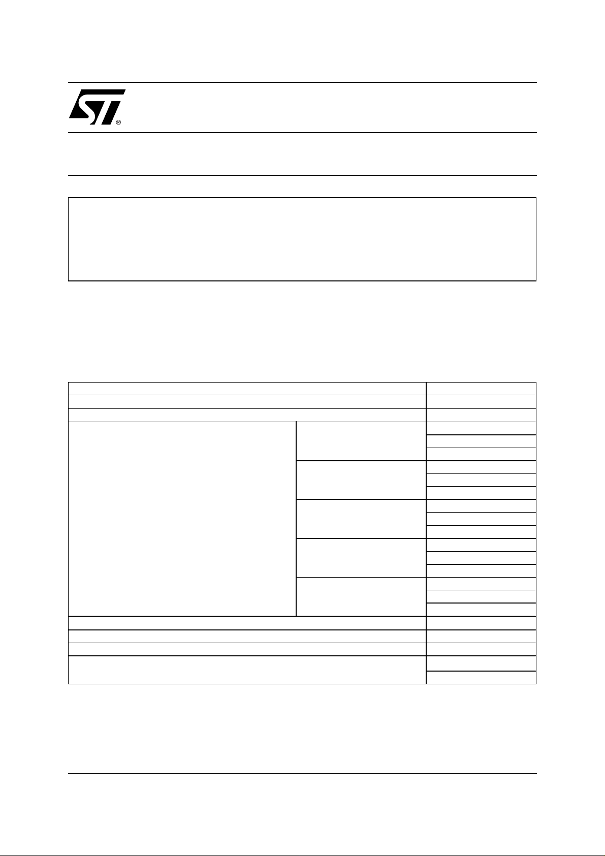
The first proposed schematic is shown in figure 1. Only its more significant features will be commented,
please refer to [2] for the standard characteristics of an L6565-based QR flyback.
Figure 1. L6565-based, EnergyStar
88 to 264
VAC
EMI
filter
C7
10 nF
F1 250VAC 5A
D1
1N4148
R1A
Ω
68 k
R6A
Ω
1.5 M
R6B
1.5 M
Ω
15 k
R7
6.2 k
68 k
R8
R1B
BD01
STBR606
Ω
47 k
1N4148
5
8
7
IC1
L6565
C6
4.7 µF
4
6
2
3
Ω
1
Ω
®
compliant, 90W SMPS for CRT monitor: electrical schematic
C8A,B 4.7 nF Y2
R13A,B 4.7 M
Ω
18
17
16
15
14
13
12
11
10
1
2
D8 UF4002
D9 UF4002
D10 UF4002
R17
Ω
2.7 k
22 nF
3
D6 UF4006
D7 STTH1L06
C14
470 µF
25V
C15
470 µF
25V
C17
C9
220 µF
100V
R18
10 k
R21
4.7 k
1000 µF
Ω
100 k
Ω
TR1
C12
16V
33 k
R15
Ω
C16
47 µF
25V
200V
R14
L1 1µH
C10
100 µF
250V
IC4
R20
330 k
L78L05CZ
R16
47
Ω
C18
15 nF
250V
R19
1.8 k
Ω
Ω
100 k
1W
C11
22 µF
100V
123
Ω
0.33A
Ω
80V
0.13A
GND
6.3V
0.6A
+15V
0.33A
5V
0.05A
C13
2.2
µF
10V
-15V
0.33A
Ω
STP6NK60ZFP
Ω
IC2
PC817A
C2
47 nF
250V
R4
1 k
Q1
1
4
7
Ω
8
4
312
IC3
TL431
C1
220
400V
R5
Ω
D4
µF
C3
47 µF
25V
DZ1
18V
0.5W
R10
1 k
C5
100 pF
4.7 k
1N4148
R12
R2
47 k
Ω
3W
D2
STTH1L06
D3 1N4148
C4 330 pF
100V
D5
R9
Ω
33
Ω
R11A,B
0.56
Ω
R3
22
2/9
Page 3
AN1657 APPLICATION NOTE
The converter is started up by R1A, R1B and the diode D1 that draw some current from the AC side of the
bridge rectifier. This inexpensive circuit wakes up the system in less then 3s @ 88 VAC and contributes
to light load losses with 240 mW @ 264 VAC. Despite this dummy consumption it is anyway possible to
meet the target of less than 2W input consumption thanks to the favorable features of the L6565. Supplying the IC from the AC side of the bridge helps reduce the power consumption on the start-up resistors
and eliminates any chance of spurious restarts at converter's power down.
R6A and B along with R7 correct the overcurren t setpoint so as to minimize the power capab ility change of
the converter over the entire input voltage range. C7 filters out any noise that might be coupled to the pin.
R8 and C6 provide soft-start. At start-up C6 is charged by the output of the L6565 E/A (pin 2) with a current
defined by 2.5 / R8 and the E/A works temporarily closed-loop. As the E/A saturates high there is no more
current through C6, the loop opens, the v oltage on pin 1 (E/A input) goe s to zero and pi n 2 s tay s high at
about 6V. When the L6565 turns off (because its supply voltage Vcc goes below the UVLO threshold) the
capacitor is discharged internally in few milliseconds - because the impedance of the pins becomes low in this way ensuring a correct soft-start even when the L6565 is continuously restarted (e.g. in case of
overload or short circuit).
Output voltage regulation is done with a TL431+optocoupler arrangement on the secondary side and the
information is fed back to the c urrent se nse pin (# 4) of the L6565. Regulation is thus performed by modulating the voltage offset generated by the phototransistor current on R10. C5 adds a small filtering effect
to increase noise immunity. This feedback arrangement helps reduce the load of the self-supply system
(winding 7-8, D3, R3, C3). In fact with the usual arrangement, where the phototransistor sinks current from
pin 2 (with pin 1 grounded), the reg ulation current, t ypically 3 m A at light load, adds up t o the o perating
current of the IC. With this circuit, to create about 1V offset, which is required at light load, the phototransistor needs to draw only 1 mA. This load reduction will counteract the natural decay of the self-supply voltage when the converter is lightly loaded. Please note that with this technique the ZCD masking time of the
L6565 (refer to [2] for details) is fixed at 3.5 µs.
The circ uit made up of R4, C4, D 4 and DZ1 provides o vervolta ge protec tion in ca se of fail ure of the feedback
loop. R4 and C4 smooth the waveform generated by the self-supply winding to suppress the leading edge
spike that could m isle ad the c irc uit. D urin g MOSF ET's off-tim e the w indin g gen era tes a vol tage proport ion al
to the output voltage . Thus, if the feedback loop opens (e.g. th e optocouple r f ai l s) , which causes the output
voltage to rise above the regulated value, the voltage provided by R4, C4 will increase as well. DZ1 will be
turned on and injec t an addit ion al offs et on the cu rrent sense pin afte r MOS FET's turn of f. As the v oltage on
the pin reaches 2V an internal comparator will be triggered, the L6565 will shut down and the converter will
be stopped until L6565's Vcc voltage, after falling below the UVLO threshold, goes again above the start-up
threshold. This may take some hundreds milliseconds, then the system will work in a continuous restart
mode, the energy throughput will be very low and the output voltage will not reach dangerous values.
Table 2. L6565-based 90W SMPS for CRT monitor: transformer specification
Core Philips ETD44, 3C85 Material
Bobbin Horizontal mounting, 18 pins
Air gap
Leakage inductance < 10 µH
Winding Wire S-F Turns Notes
Pri1 4xAWG29 2-4 19 Pin 4 is cut for safety
Sec1 (200V) AWG25 17-18 48
Windings
Spec & Build
Sec2 (80V) AWG25 15-16 32
Sec3 (6.5V) AWG25 13-14 3 Evenly spaced
Sec4 (+15V) AWG25 11-12 6 Bifilar with Sec5
Sec5 (-15V) AWG26 10-11 6 Bifilar with Sec4
Pri2 4xAWG29 1-2 19
Aux (+15V) AWG29 8-7 7 Evenly spaced
1 mm for an inductance 1-4 of 380 µH
≈
The linear regulator that supplies the 5V line for the µP takes its input from the +15V line. Using the 6.5V
line would improve efficiency (espec ially in OFF-mode) even furthe r. To do so, however, an LDO (low
3/9
Page 4

AN1657 APPLICATION NOTE
dropout) regulator is needed (with the L7805 at least 2V dropout must be ensured), which is slightly more
expensive, and the transformer must supply a sufficient voltage (5V plus the dropout and the tolerances)
under all operating con dit ions . Actuall y, in S us pend mode with the heater still sup plied the 6 .5V dr ops at
5.5V, which forces the use of the +15V line. Either with a better transformer construction - so that the 6.5V
line never falls below, say, 6V or turning off the heater during Suspend mode, an LDO regulator could provide 5V powered by the 6.5V line, thus reducing the converter actual load by about 150 mW.
There is no special circuit that handles the OF F-mode ope ration: simply, whe n the m onitor enters OFFmode the loads drop to negligible values on all of the outputs except the 5V one that must still supply the
µP governing monitor operation. In these condi tions µP's consumpt ion is estimated at 25 mA max. As a
result, the L6565 will enter its natural burst-mode operation, where a series of few switching cycles are
repeated at the frequency of the internal starter or at a submultiple of its. The consumption measurements
under these operating conditions are shown in table 4 in the "Experimental results" section.
"1W Initiative" compliant design
To make such design the starting point will be the EnergyStar® compliant circuit, which a circuitry dedicated
to handle the OFF -mode will be ad ded to. Bes ides the ad ditional circu itry, minimum a daptations in the power
section and some changes in the control circuit will be required. Figure 2 shows the resulting schematic.
Conceptually, the way OFF-mode is handled consists of forcing the L6565 to work in a very low frequency
controlled burst-mode (continuous restart), so as to cut all frequency-related losses . To see how this is
achieved practically it is worth examining the schematic of figure 2, specifically looking at the new and
modified parts as compared to the schematic of figure 1.
Starting from the primary side, the major addition is the high-voltage active start-up circuit (R1A, R1B, R2,
D1,DZ1 and Q1) along with the associated network (R9, R10, Q3) to turn it off when the converter is running. This addition has a not negligible impact on the part count and the total cost but is essential.
Figure 2. L6565-based, "1W Initiative" compliant, 90W SMPS for CRT monitor: electrical schematic
88 to 264
VAC
EMI
filter
R1A
4.7 M
R1B
4.7 M
D1
1N4148
DZ1
12 V
0.5W
1.5 M
1.5 M
C5
10 nF
Q3
BC547
F1 250VAC 5A
Ω
Ω
R7A
Ω
R7B
Ω
15 k
R8
Q1
STQ1NC60R
R2
Ω
6.8 k
3
Ω
1
R10
Ω
47 k
BD01
STBR606
8
IC1
L6565
C6 4.7 µF
R9 220 kΩ
R11
Ω
6.2 k
5
2
R6
47 k
1N4148
7
4
6
C8A,B 4.7 nF Y2
R16A,B 4.7 M
C1
220
400V
Ω
D4
µF
C3
47 µF
25V
DZ2
18V
0.5W
1N4148
R13
1 k
C7
100 pF
R15
4.7 k
R3
47 kΩ
3W
STTH1L06
D3 1N4148
C4 330 pF
100V
D5
R12
33
Ω
Ω
Ω
D2
R4
22
R14A,B
0.56
47 nF
250V
Ω
STP6NK60ZFP
Ω
IC2
PC817A
C2
R5
1 k
Q2
1
4
7
Ω
8
4
312
1
2
18
17
16
15
14
13
12
11
10
Ω
2.7 k
3
R20
TL431
D6 UF4006
D7 STTH1L06
D8 UF4002
D9 UF4002
C13
2200 µF
25V
C14
470 µF
25V
D10 UF4002
Ω
R21
Ω
10 k
C16
22 nF
IC3
C9
220 µF
100V
R24
4.7 k
1000 µF
100 k
330 k
Ω
C12
16V
TR1
R23
33 k
DZ3
10V
0.5W
R18
Ω
200V
Ω
R26
470
C18
470 nF
0.33A
80V
0.13A
GND
6.5V
0.6A
+15V
0.33A
5V
0.05A
C15
µF
2.2
10V
-15V
0.33A
OFF
Ω
R17
DZ4
10 k
Ω
R27
100 k
1W
C11
22 µF
100V
IC4
LE50CZ
123
Ω
L1 1µH
C10
100 µF
250V
Ω
R19
680
C17
15 nF
250V
R22
Ω
1.8 k
R25
Ω
5.6 k
8.2V
0.5W
Q4
Ω
BC547
4/9
Page 5

AN1657 APPLICATION NOTE
The importance of the c ircuit lies not on ly in the reduction of the associate d losses from the 24 0 mW of
the resistive start-up to less than 10 mW, but also in the fact that, arranged as a current source like in the
schematic of figure 2, it provides constant wake-up and restart times for the converter, regardless of the
input AC voltage. The benefits resulting from that will be clearer after discussing how the system handles
OFF-mode operation. The current sourced by the generator and that charges the V
I
CH
VZVFVth–+
---------------------------------- -=
R2
,
where VZ is the zener voltage of DZ1, VF the forward drop across D1 and Vth the threshold voltage of Q1.
With an appropriate selection of V
°C) and Vth (≈ -7 mV/°C). Experience s hows t hat z en er dio des wi th V
it is possible to compensate the temperature drift of both VF (≈ -2 mV/
Z
=12V have a temperature coeffi-
Z
cient around +10 mV/°C, thus one of them will be selected.
With this circuit, neglecting the start-up current abs orbed by the L6565, which is typically two orders of
magnitude smaller, the wake-up time is defined by R2, C3 and the turn-on threshold (V
C3
-------- -
T
wake up–
V
≈
I
CH
CCOn
,
capacitor C3 is:
CC
) of the L6565:
CCOn
whereas the restart time, that is the time needed for Vcc to go from the UVLO threshold (V
during a continuous restart, depends on the VCC hysteresis (V
C3
T
Restart
-------- -
V
≈
I
CH
CCHys
CCHys
.
= V
CCOn
- V
) of the L6565:
CCOn
CCOff
) to V
CCOn
The circuit that is actually responsible for handling OFF-mode operation is on the secondary side and is
the network comprising R25 to R27, C18, DZ4 and Q4. To adapt the existent circuit to the new operation,
R19 (R16 in the schematic of fig. 1) has been increased to 680Ω and the capacitor C13 has been replaced
by the zener diode DZ3. The bulk capacitor C13 on the +15V line has been increased from 470 to 2200µF
and the L7805 replaced by an LE50CZ.
During normal operation a logic signal (open collector) governed by the µP keeps the OFF input low, so
that Q4 is always off and the OFF-mode c ircuit is disabled. When t he monitor is to enter OFF-m ode the
µP acts so that the loads of all the outputs are cut off, then it reduces its own consumption and opens the
pull-down that was grounding the OFF input. Q4 is imm ediately turned on because t he voltage on the
+15V is already higher than threshol d (V
) defined by DZ4, R2 5 and R27. Q4 will then d raw a relat ively
T
large current from the photodiode, limited by R19+R20 (that is why C13 has been replaced by DZ3: this
will still give a high frequency pole to the output-to-control transfer function but will keep the current
through the photodiode under control as Q4 is turned on).
As a result there will be quite a large current in the phototransistor too, which will bring the voltage on the
current sense pin above the 2V threshold that shuts down the driver of the L6565 and stops PWM activity.
The IC, however, remains act ive and pin 2 stays high , thus keeping the start-up generator off as l ong as
Vcc - which is decaying because of the quiescent consumption of the IC and the phototransistor current is above V
. As VCC = V
CCOff
the IC turns off, pin 2 goes low and the start-up generator is turned on
CCOff
again.
This is the most critical moment: since the output voltage starts from about 15V and needs to decay below
before Q4 turns off, the phototransis tor will k eep on sinking quite a la rge c urrent even after the st art-
V
T
up generator is enabled. As a result, V
a time longer than T
to bring VCC back to V
Restart
will be pulled well below V
CC
and restart PWM activity. On the secondary side,
CCOn
. The start-up generator will take
CCOff
as the L6565 stops switching the voltage on C13 starts to decay slowly and goes on like that as long as
the L6565 does not switch. Even during this time the voltage on C13 must not go below the minimum value
that correctly supplies the linear regulator. To have maxim um headroom the LE50CZ has been used,
which features less than 0.5V dropout. Besides, this part has lo wer quiescent current and t he l ow dropout
allows keeping a lower average input voltage, which helps reduce the actual load on the converter.
As PWM restarts, the voltage on C13 quickly builds up and reaches VT in few milliseconds, which turns on
Q4 again restarting another cycle. C18 filters switching noise and allows a clean Q4 turn-on. This time the
phototransistor current will drop to zero before Vcc falls below V
and there will be no VCC undersho ot .
ccOff
5/9
Page 6

AN1657 APPLICATION NOTE
Under steady-state operation the L6565 will be then shortly activated with a repetition rate T
given by T
Decay
+ T
Restart
, where T
is the time that VCC takes to span VCC hysteresis downward:
Decay
C3
------- -
T
Decay
V
≈
CCHys
I
q
,
essentially
Rep
and Iq is the quiescent consum ption of the L6565. The input of the linear regu lator is a sawtooth go ing
from a peak ≈V
a sawtooth going up and down from V
to a valley that depends on T
T
CCOn
, C13 and the input current to the LE50CZ . Al so Vcc is
Rep
to V
CCOff
.
When the monitor is to resume its normal operation the OFF input will be grounded thus inhibiting Q4 and
disabling the OFF-mode circuit. However, the L6565 will be able to respond only when it is active. Under
the worst-case conditions, that is the OFF in put is grounded just after the IC has been shu t down, the
L6565 will be responsive only after a time T
count, re-enabling the loads on all of the outputs with a delay not shorter than T
. The power management software must take this into ac-
Rep
after grounding the
Rep
OFF input.
Experimental resu lts
In the following tables the results of some benc h evaluations are sum marized. Some wavef orms at full
load and off-mode under different line conditions are shown for user's reference, with some stress on the
OFF-mode management of the "1W initiative" compliant design.
As to the full-load performance there is no significant difference between the two designs presented: table
3 is common to both. Same applies to table 4 tha t shows the c onsum ption during Suspend-mode operation, a particular low-consumption mode envisaged by VESA standards. No specia l action i s taken to keep
the consumption below the limit (Pin < 15W): the converter can comfortably fulfill this requirement.
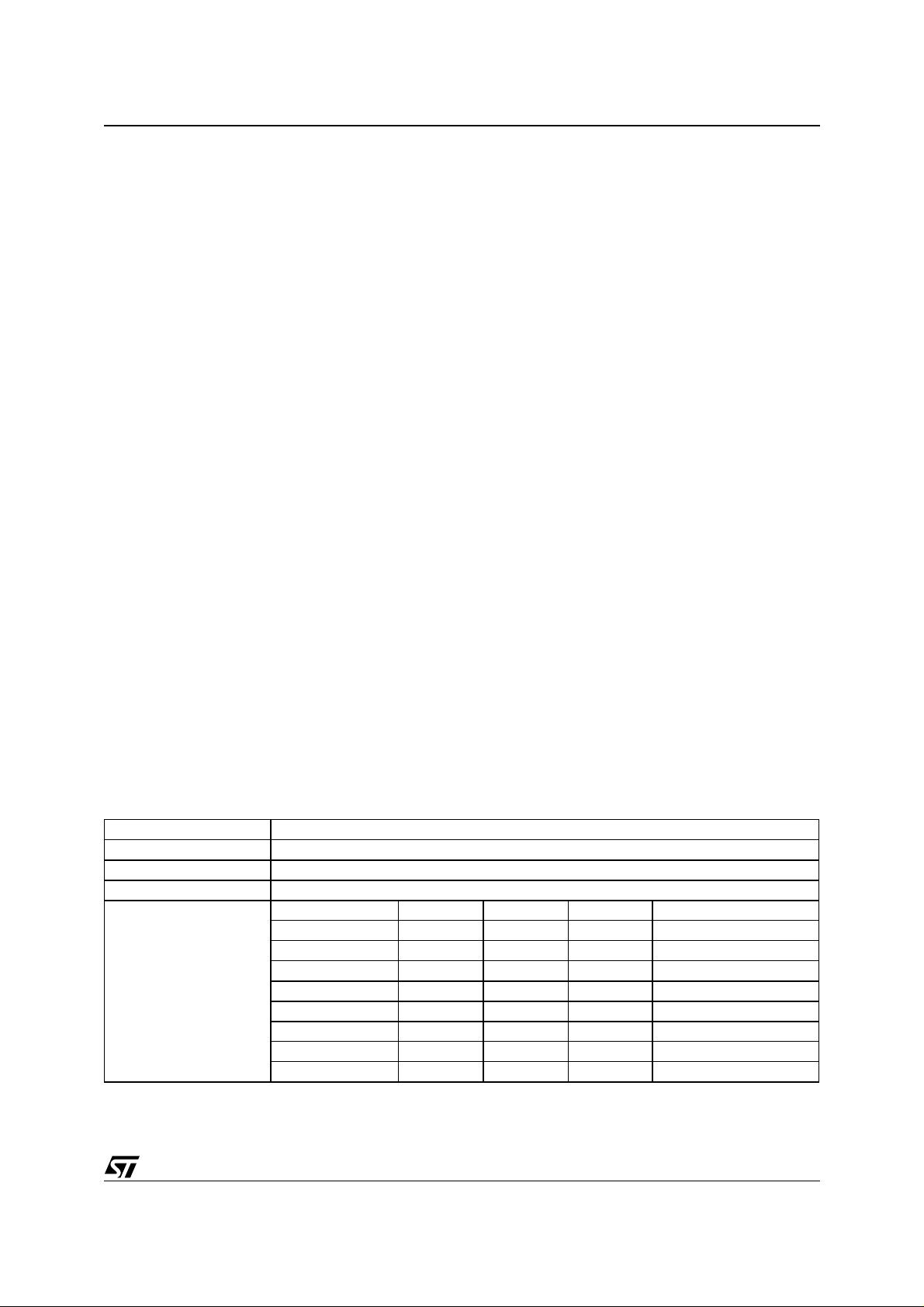
Table 3. L6565-based, 90W SMPS for CRT monitor: line regulation and full load efficiency
VAC [V]
Pin [W] 103.9 101.0 99.6 98.4 98.4 98.6
Vout [V]
Pout [W] 90.59 90.61 90.63 90.64 90.69 90.69
η [%] 87.2 89.7 91.0 92.1 92.2 92.0
Load conditions: 200V: 0.33A; 80V: 0.13A; ±15V: 80 Ω; 6.5V: 10Ω; 5V: 0.05A
88 110 132 176 220 264
199.90 199.87 199.84 199.83 199.86 199.82
79.45 79.40 79.3 9 79.37 7 9.38 79.39
14.12 14.13 14,1 4 14.14 1 4.16 14.16
-14.20 -14.20 -14.2 1 -14.21 -1 4.22 -14 .22
6.58 6.60 6.62 6.63 6.64 6.65
Table 4. L6565-based, 90W SMPS for CRT monitor: Suspend-mode con sump tion
V
[V]
AC
Pin [W] 12.6 12.9 13.3 13.3 13.4 13.6
Load conditions: 200V: 0.005A, 80V: 0.065A; ±15V = open; 6.5V: 10Ω (heater on); 5V: 0.025A. Pout ≈ 9.3W
Pin [W] 8.3 8.3 8.5 8.5 8.6 8.7
Load conditions: 200V: 0.005A, 80V: 0.065A; ±15V = 6.5V = open (heater off); 5V: 0.025A (LDO regulator supplied
from 6.5V line). Pout ≈ 6.3W.
Note: a) Applicable to EnergyStar
b) Efficiency improvement is due to onset of L6565 burst-mode operation.
88 110 132 176 220 264
compliant design only.
6/9
Page 7

AN1657 APPLICATION NOTE
Table 5. L6565-based, EnergyStar® compliant design: OFF-mo de consump tio n
VAC [V]
Pin [W] 1.4 1.4 1.4 1.4 1.5 1.6
Load conditions: 200V = 80V = ±15V = 6.5V = open; 5V: 0.025A. Pout = 0.125W
Pin [W] 1.2 1.2 1.2 1.2 1.3 1.4
Load conditions: 200V = 80V = ±15V = 6.5V = open; 5V: 0.025A (LDO regulator supplied from 6.5V line)
Table 6. L6565-based, "1W Iniziative" compliant design: OF F-mod e con sump tio n
V
[V]
AC
Pin [W] 0.25 0.31 0.38 0.49 0.62 0.75
Load conditions: 200V = 80V = ±15V = 6.5V = open; 5V: 0.025A. Pout = 0.125W
Figure 3. Line filter (not tested for EMI compliance) used during prototype bench evaluation
88 110 132 176 220 264
88 110 132 176 220 264
to the AC
source
B81133
470 nF, X2
EPCOS
B82732
47 mH, 1.3A
EPCOS
B81133
680 nF, X2
EPCOS
to the
SMPS
Figure 4. L6565-ba sed, 90W S MPS f or CRT mon itor: Full load, Vin=100 VDC (lef t), Vin=380 VDC (right)
Q1 Drain
Q1 Drain
Figure 5. L6565-based, 90W SMPS for CRT monitor: Open feedback and OVP, main wavefo rms
200V Output
Smoothed auxiliary
winding
Pin 4 of L6565
Gate drive
Smoothed auxiliary winding
Pin 4 of L6565
7/9
Page 8

AN1657 APPLICATION NOTE
Figure 6. L6565-based, EnergyStar® design: OFF-mode, Vin = 100 VDC (left), Vin = 380 VDC (right)
L6565 Vcc
Q1 Drain
L6565 Vcc
Q1 Drain
Figure 7. L65 65- bas ed, "1W Initiat i ve" com pl i a nt des i gn : OFF -mode main waveforms
L6565 Vcc
V (C13)
Pin2 L6565
L6565 Off
HV gen. On
Phototr. On
L6565 Off
HV gen. On
Phototr. Off
lowest vall ey
Q1 Drain
L6565 Vcc
V (C13)
Pin2 L6565
Q1 Drain
Figure 8. L6565-based, "1W Initiative" compliant design: entering (l eft) and exiting (right) OFF- mode
8/9
Q1 Drain
V (C13)
Pin2 of
L6565
Vcc of L656 5
Soft-start
Vcc of L6565
Collector
of Q4
Pin4 of
L6565
Page 9

AN1657 APPLICATION NOTE
Conclusions
Two designs of a CRT m onitor S M PS based on the QR con troller L65 65 have been realized and th e results of their bench evaluation have been presented. The first one is a low-cost design able to meet current
EnergyStar
slight part count and cost increase, me ets the target Pin <1W , which makes it compl iant with IEA's "1W
initiative" as well as eligible for GEEA label.
REFERENCES AND RELATED DOCUMENTATION
[1] "L6565 QUASI-RESONANT SMPS CONTROLLER" DATASHEET
[2] "L6565 QUASI-RESONANT CONTROLLER" (AN1326)
[3] "25W QUASI-RES ONANT FLY BACK CONVER TER FO R SET-T OP BOX A PPLICA TION U SING T HE
L6565" (AN1376)
[4] "EVAL6565N, 30W AC-DC ADAPT ER WITH T HE L6565 QUASI-RESONANT PW M CONT ROLLE R"
(AN1439)
®
requirements on OFF-mode consumption (Pin < 2W). The second design , at the price of a
Information furnished is believed to be accurate and reliable. However, STMicroelectronics assumes no responsibility for the consequences
of use of such information nor for any infringement of patents or other rights of third parties which may result from its use. No license is granted
by implic ation or otherwise under any patent or patent r i ght s of STMi croelectr oni cs. Specifications menti oned in thi s publicati on are subj ect
to change without notice. This publication supersedes and replaces all information previously supplied. STMicroelectronics products are not
authorized for use as cri tical components in li f e support dev i ces or systems without express writ t en approval of STMicroel ectronics.
STMicroelectronics acknowl edges the trademarks of all companies referred to in this document.
The ST logo is a registered trademark of STMicroelectronics
© 2003 STMic roelectroni cs - All Rig hts Reserved
Austra lia - Brazil - Canada - Ch i na - F i nl and - France - Germany - Hong Kong - India - Israel - Italy - Japan -Malay si a - Malta - Morocco -
Singap ore - Spain - Sw eden - Switzerland - Uni ted Kingdom - United St ates.
STMicroelectronics GROUP OF COMPANIES
http://www.s t. com
9/9
 Loading...