

AN1645
Obsolete Product(s) - Obsolete Product(s)
APPLICATION NOTE
STSR2P/STS R2PM SIMPLIFIES IMPLEMENTATION OF
SYNCHRONOUS RECTIFIE RS IN FORWARD CON VERTER
F. Librizzi - F. Lentini
1. ABSTRACT
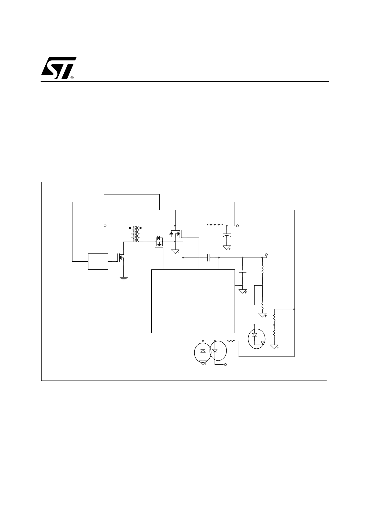
This paper describes t he functionality and the operation of t he STSR2P devi ce used as the s econdary
synchronous rectifier driver in Forward t opolog y switched mo de powe r su pplies. A s chem at ic and l ayout
description of a demo board, able to replace d iode rectification with s ynchronous rectification in Forward
converters, is shown below.
Figure 1: Typical Application Schematic
Feedback
Loop
TRANSFORMER
PWM
2. GENERAL DEVICE DESCRIPTION
MosfetN
Q1
MosfetN
Q2
1
8
OUTGate1
PWRGND
STSR2
option
P
D1
7
OUTGate2
5
INDUCTOR
Cout
100nF
INHIBIT
2
Vcc
SGLGND
SETANT
D2
+5V
VoutVin
+5V
100nF
6
3
4
Ck
D3
R5
+5V
R1
R2
R3
R4
The STSR2P Sm art Driver IC provi des two compl ementary high current ou tputs to drive Po wer Mosfets.
The IC is dedicated t o properly drive secondary Synchronous Rectifiers in medium power, low output
voltage, high efficiency Forward Converters. From a synchronizing clock input, the IC generates two
driving signals with a certain dead time between complementary pulses. The adopted transitions
December 2003 (rev.1)
1/22
Obsolete Product(s) - Obsolete Product(s)
AN1645 - APPLICATION NOTE
revelation mechanism makes circuit operation independent by the forward magnetic reset technique
used, avoiding most of the common problems inherent in self-driven synchronous rectifiers. The IC
operation prevents secondary side shoot-th rough conditions providing proper timing at the ou tputs turnoff transition. This smart function operates through a fast cycle-after-cycle control logic mechanism
based on an intern al hig h fre quenc y os cillator, synchronized by the clock signal. The I C prov ides a fixed
anticipation in turning-off the OUTGate1 with respe ct to the clock signal transition, while the anticipation
in turning-off the OUTGate2 can be set through external components. A speci al Inhibit function allows
the shut-off of one of the two outputs allowing operation during discontinuous conduction mode and
preventing the freewheeling mosfet from sinking current from the output.
The STSR2P automatically turns off the outputs when duty-cycle is lower than 13%, while STSR2PM
works even at very low duty-cycle values.
.
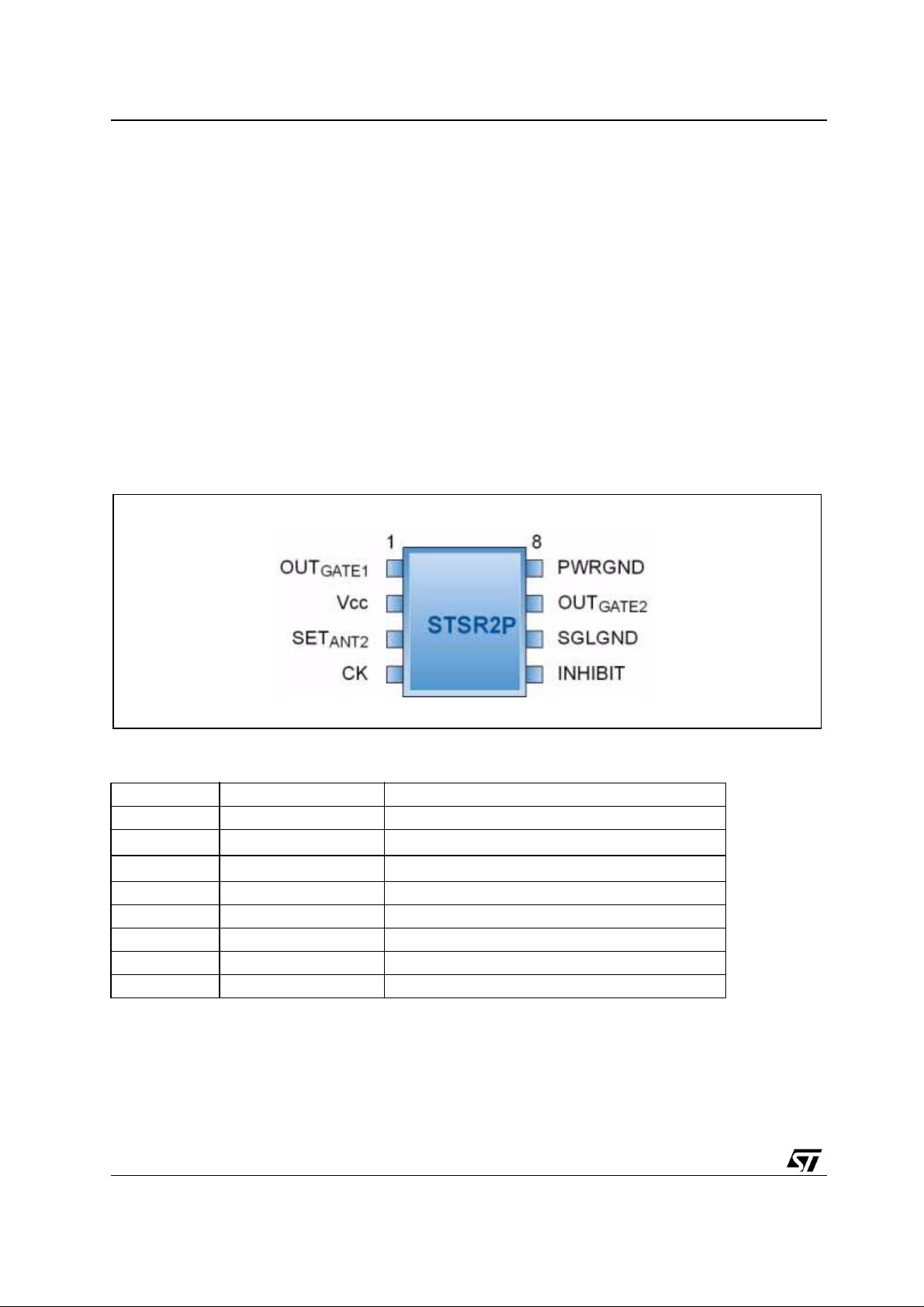
3. PIN CONNECTIONS AND DESCRIPTIONS
The STSR2P is housed in a SO-8 package for SMD assembly. Device pin out is shown in figure 2 and
table 1 briefly summarizes the device pin functionality.
Figure 2: Pin Configuration
Table 1: Pin Configuration
Pin Number Pin Name Pin Function
1 OUTGate1 Output for Forward MOSFET Gate Drive
2 Vcc Supply input from 4V to 5.5V
3 SETANT
4 CK Synchronization for IC’s operation
5 INHIBIT Discontinuous Mode Detector
6 SGLGND Reference for all the control logic signals
7 OUTGate2 Output for Freewheeling MOSFET Gate Drive
8 PWRGND Reference for power signals
2
Sets the anticipation in turning-off the OUT
GAT E2
2/22
Obsolete Product(s) - Obsolete Product(s)
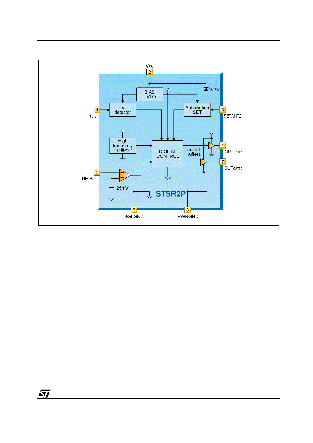
Figure 3: Block Schematic
AN1645 - APPLICATION NOTE
4. SUPPLY VOLTAGE AND UNDER VOLTAGE LOCK-OUT
The supply input range is from 4V to 5.5V. An internal zener diode limits the maximum voltage to 5.7V .
A 100nF ceramic capacitor must be connected to Vcc and SGLGND pin in order to assure a stable
supply voltage. This capacitor must be placed very close to the device. Another 100nF capacitor is
necessary between Vcc and PWRGND.
Under Voltage Lock Out feature guarantees p ro per start-up while it avoid s undesirable driving during
eventual dropping of the supply voltage.
As shown in the Block Diagram, the V cc voltage also supplies the two out put drivers, consequent ly the
maximum driving voltage is 5.5V, so the use of logic gate threshold mosfets is recommended.
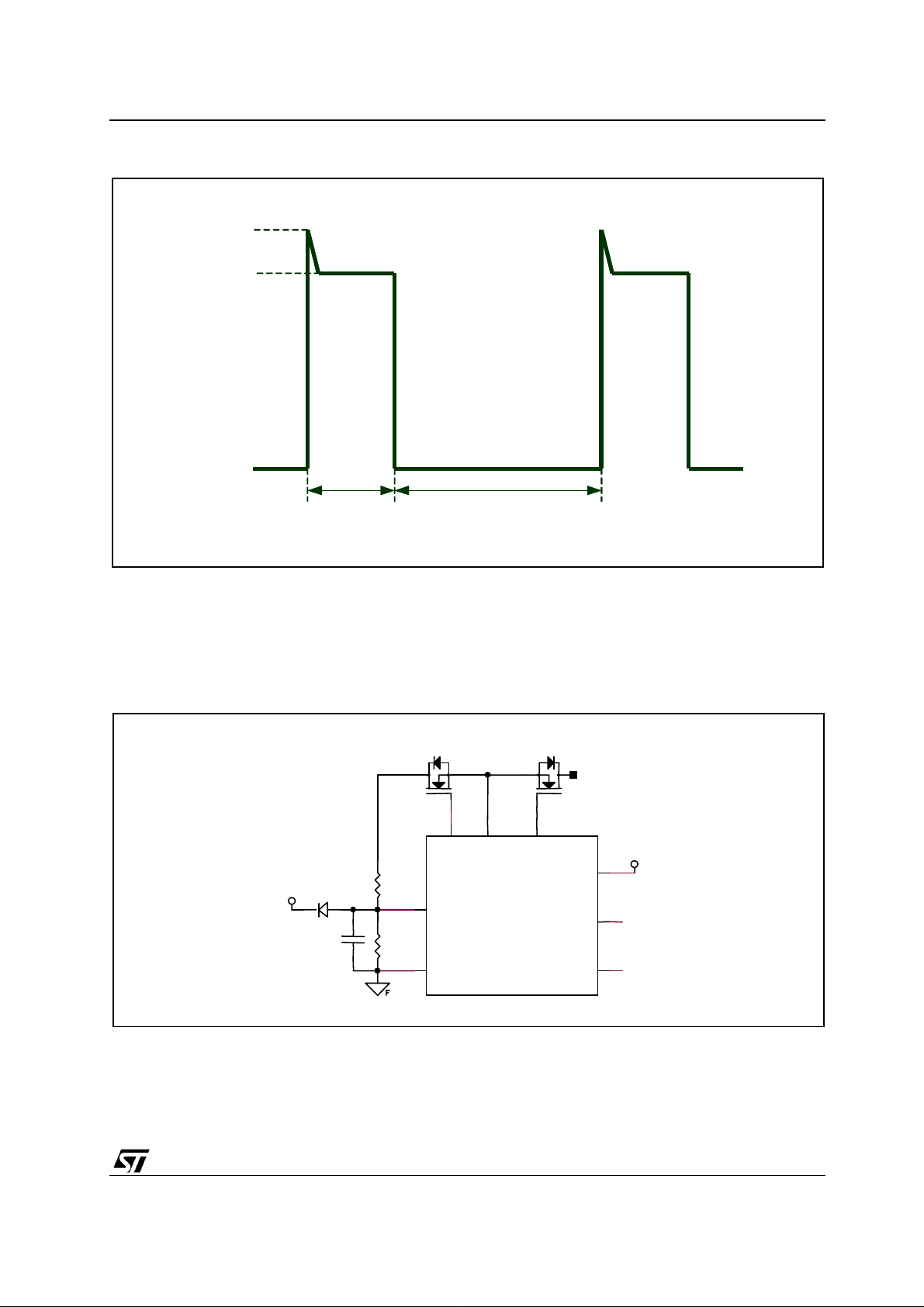
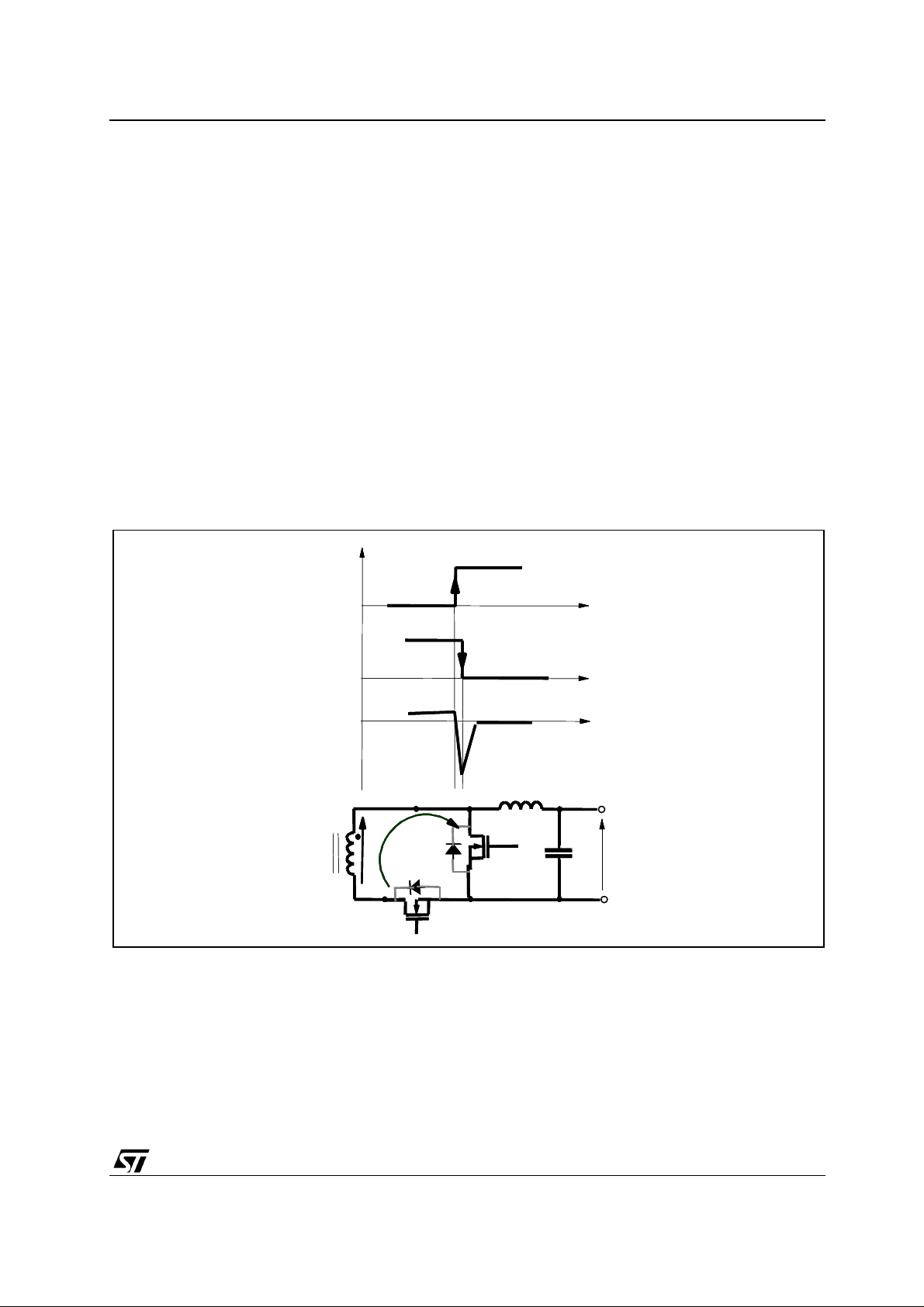
5. SYNCHRONIZATION
An innovative feature of the STSR2P is the capability to operate in the secondary side without any
synchronization signal coming from the primary side. The IC synchronization is obtained directly from the
secondary side using the voltage across the free wheeling mosfet as the information f or the switching
transitions. The Ck pin is the input for the synchronization signal; t he internal thresho ld is set at 2.8V. As
can be seen in figure 3, a Peak Detector is present at the Ck pin. This block is able to distinguish
between the primary mosfet switching transitions and the eventual sinusoidal waveform caused by
discontinuous mode operation (see figure 4). A wrong synchronization causes wrong driving of the
synchronous rectifiers.
3/22
Obsolete Product(s) - Obsolete Product(s)
AN1645 - APPLICATION NOTE
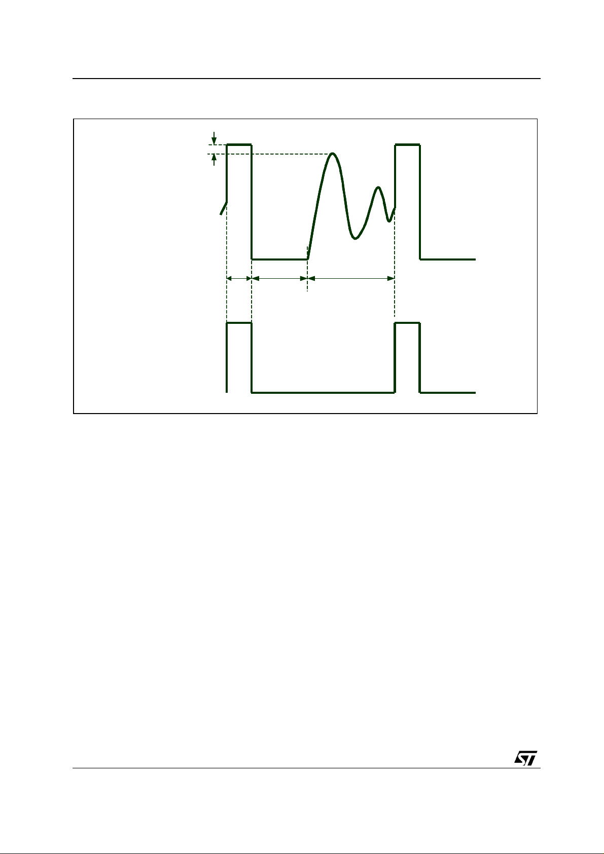
Figure 4: DCM waveform
V
V
1
1
Peak
Peak
Detector
Detector
Input
Input
Peak
Peak
Detector
Detector
Output
Output
On
On
Time
Time
Off Time Dead Time
Off Time Dead Time
5.1 Continuous Conduction Mode
When the converter is working in continuous mode the voltage ac ross the source and drain of t he free
wheeling mosfet has a square shape. This voltage can be applied to the Ck pin using two different
configurations: with a resistor divider (figure 6) or with a diode and pull-up resistor (figure 7). In most
cases a spike is present during turn-off of the synchronous m osfet; this spike m ust be eli minated at t he
Ck pin in order to avoid false synchronization.
Using the resistor divider , the spike is eliminated by adding a small capacitor (C1) as shown in figure 6.
4/22
Obsolete Product(s) - Obsolete Product(s)
Figure 5: CCM waveform and Ck circuit
Turn-Off
Turn-Off
Spike
Spike
On Time Off Time
On Time Off Time
AN1645 - APPLICATION NOTE
In a typical Forward converter for telecom application, the DC input voltage has a 1:2 va riability range
(typically 36V-72V). Consequently the secondary winding voltage has also 1:2 variability. The resistor
divider can be calculated in order t o have about 2.8V at the Ck pin at 36V inp ut; at 72V in put, t he Ck pi n
reaches 5.6V. Even if this value is higher than the maximum voltage on the CK pi n, it can be accepted
limiting the current flowing into the pin to 10mA.
Figure 6: Synchronization with a resistor divider
FREE WHEEL FORWARD
1
+5V
2
PWRGND
OUTGate1
SETANT
INHIBIT
Vcc
3
5
+5V
D1
C1
R1
R2
4
6
7
OUTGate2
Ck
SGLGND
8
STSR2P
In case the Forward converter has a higher variability range 1:3 or 1:4, at minimum input voltage, 2.8V
must be guaranteed at the Ck pin. At maximum input voltage, the voltage at the Ck pin will be 7.5V or
10V. This voltage exceeds the absolute maximum ratings of the device. If R2 limits the current flowing
into the Ck pin to a va lue below the maximum Ck current value indicated in t he datasheet (10mA), the
5/22
Obsolete Product(s) - Obsolete Product(s)
AN1645 - APPLICATION NOTE
device can still working properly; otherwise a diode D1 connected to Vcc or a zener diode must be added
to protect the device.
Figure 7: Synchronization with a diode and pull-up resistor
+5V
FREE WHEEL
D1
R1
4
6
7
OUTGate2
Ck
SGLGND
8
PWRGND
STSR2P
1
OUTGate1
SETANT
INHIBIT
FORWARD
Vcc
+5V
2
3
5
Figure 7 shows the synchronization circuit with diode and pull-up resistor. In this case there is no
problem with the turn-off spike and maximum CK pin voltage. This circuit cannot work properly in
Discontinuous Mode due to the ringing present in the voltage drain of the synchronous rectifier.
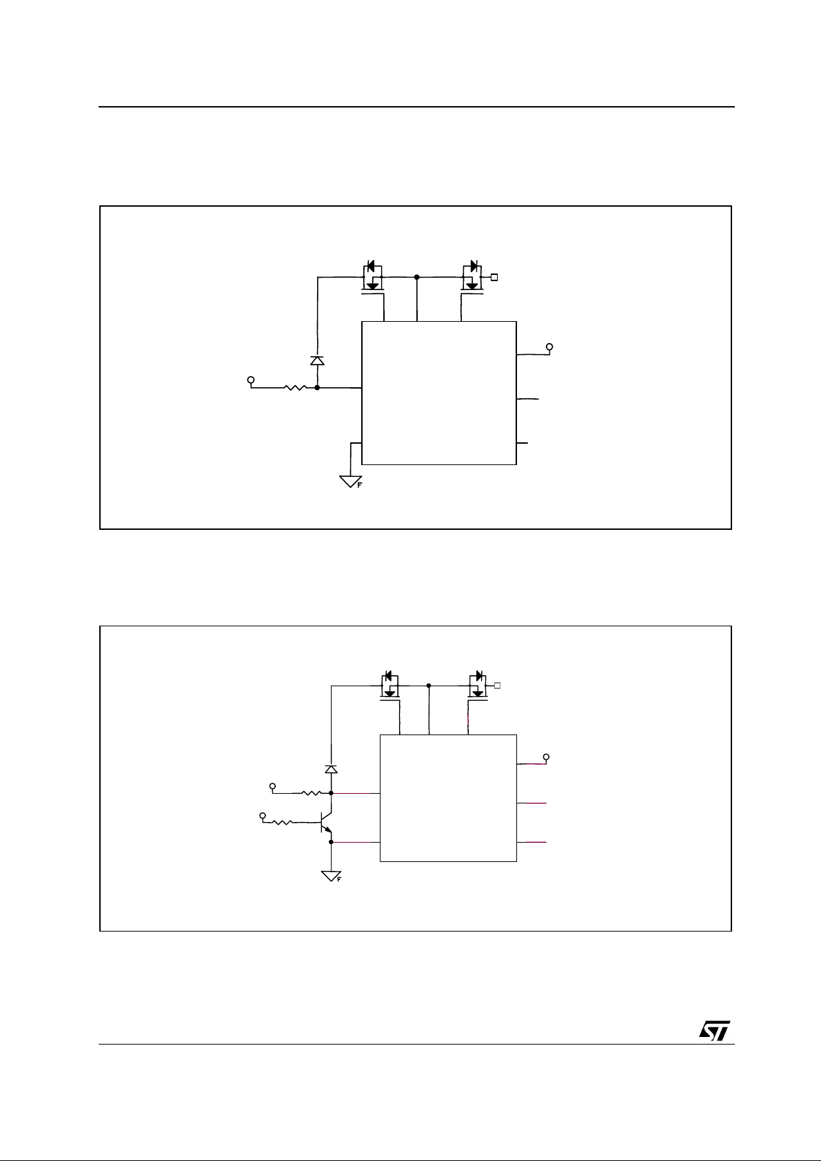
Figure 8: Shut-down circuit
FREE WHEEL FORWARD
1
8
7
D1
R1
+5V
OFF
R2
The STSR2P can be easily turned off adding a NPN transistor between Ck and SGLGND. This transistor
Q1
NPN
4
6
Ck
SGLGND
PWRGND
OUTGate2
STSR2P
OUTGate1
SETANT
INHIBIT
Vcc
+5V
2
3
5
forces the CK pin to GND wh en the sign al OFF is high . In this condition O UTGate1 and O UTGate2 wil l
be in a low state turning off the Synchronous Mosfets.
6/22
Obsolete Product(s) - Obsolete Product(s)
AN1645 - APPLICATION NOTE
Figure 8 shows the turn-off circuit when using a diode and pull-up resistor to synchronize the STS R2P,
the same configuration of Q1 and R2 can be used with a resistor divider circuit.
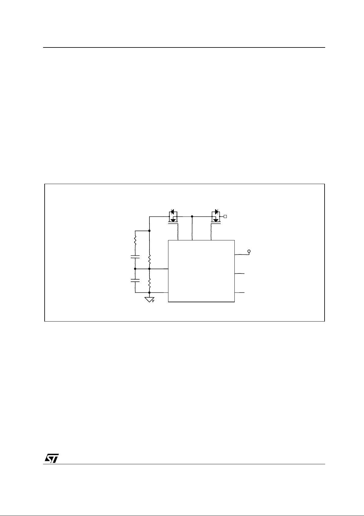
5.2 Discontinuous Conduction Mode
As shown in figure 4, in d iscontinuous mode operation there can be some proble ms in detecting the
primary switching transitions. The internal peak detector is only able to determine the peak value
reached by the signal at the Ck pin, neglecting all signals that have a lower value. A minimum voltage
difference V1=400mV between the switching transition waveform and the sinusoidal waveform must be
assured in order to allow the Peak Dete ctor to work properly. If the ringing presents almo st the same
value as the square w aveform, it is pos sibl e to add a filter circuit to the CK pin in order to obtain a be tter
operation. This circuit is showed in figure 9. R1-R2 and C2 form a low pass filter, which allows a reduction
of the ringing am plitude. But R1-R2 and C2 also cause an undesired delay, so the R3 and C1 group
reduce this delay during fast switching transitions.
Figure 9: Fi lter to C K input
FREE WHEEL FORWARD
PWRGND
STSR2P
1
OUTGate1
SETANT
INHIBIT
Vcc
+5V
2
3
5
R3
C1
C2
R1
R2
4
6
7
OUTGate2
Ck
SGLGND
8
As mentioned in the previous paragraph, if the input voltage variability range is higher than 1:2, at high
voltage the signal at the CK pin will be clamped. In these conditions, both switching transition waveform
and the sinusoidal waveform are clamped and the peak detector is unable to operate correctly (see figure
10). In this case it is possible to use an external signal, which turns off completely the device in no load or
light load conditions (figure 8).
7/22

Obsolete Product(s) - Obsolete Product(s)
AN1645 - APPLICATION NOTE
Figure 10: DCM clamped
V
V
CC
CC
Peak
Peak
Detector
Detector
input
input
On
On
Time
Time
Peak
Peak
Detector
Detector
output
output
Off Time
Off Time
Dead Time
Dead Time
6. INHIBIT OPERATION
One of the differences between diode rectification and synchronous rectification is the possibility for
Mosfets to conduct the current in both directions while diodes conduct just in one direction. In
discontinuous mode with d iode rectification, when the inductor current reaches zero it cannot reverse
because the diode does not allow current flowing from c athode to anode. Using mosfets as rectifiers,
when the inductor cu rrent reaches zero, it continues to decrease becoming neg ative and flowing from
drain to source of the freewheeling mosfet. In this condition the converter works always in con tinuous
mode.
If discontinuous mode operation is required, the freewheeling mosfet must be turned off when the current
is zero, consequently th e body diode operates as a com mon rectifier avoiding reversal of the inductor
current.
The INHIBIT pin is able to turn off the freewheeling mosfet when its current is approaching zero allowing
discontinuous mode operation of the converter.
On the INHIBIT pin, there is an internal comparator with a -25mV threshold. This pin is connected
through a resistor to the drain of the freewheeling mosfet. At the beginning of the off time (when Ck goes
to low level), OUTGate
is higher than -25mV, OUTGate
is kept high until the voltage reaches -25mV. This is because when the freewheeling mosfet is
conducting, the voltage on its drain is: Vds= -Rds(on)*Idrain. If Vds is higher than -25mV, it means that
the current is decreasing and d iscontinuous mode is approachi ng, so OUTGate
operation of the body d iode of the mosfet (see figure 11). When the converter is in cont inuou s mod e t he
INHIBIT voltage is always lower than -25mV and OUTGate
mosfet occurs when the current is not exac tly zero, the remaining amount of current is dependent on
R
of the mosfet.
DS(on)
goes high. The INHIBIT voltage is monitored for 250ns: if the voltage on INHIBIT
2
becomes low; if the voltage on INHIBIT is lower than -25mV, OUTGate
2
is turned-off allowing
2
is kept high. The turn off of the freewheeling
2
2
8/22
Obsolete Product(s) - Obsolete Product(s)
AN1645 - APPLICATION NOTE
During tr ansit ion in whic h the p rimary mosfet is turned off, the INHIBIT voltage must fall from high value
to -25mV in less than 250ns. The resistor value R26 must be chosen in order to fit this specification.
When the converter operates in parallel with other power supplies, the INHIBIT pin, detecting the voltage
across the freewheeling mosfet, also avoids the converter to sink current from the output.
Although the INHBIT pin allows operation in Discontinuous Mode, the -25mV threshold could be sensitive
to the ringing present at the SR Mo sfet drain (see figure 13), caus ing incompl ete turn on of OUT Gate2.
This inconvenience can be avoided using the clock signal to provide a negative voltage to the INHIBIT
pin acting as a blanking time. This negative voltage can be easily generated with some discrete
components as shown in figure 12.
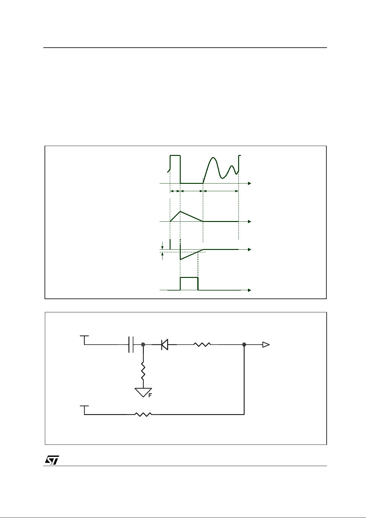
Figure 11: INHIBIT Voltage and Current
Freewheeling
source-drain
voltage
On Time
Inductor
Current
INHIBIT
Voltage
-25mV
Freewheeling
Gate Voltage
Figure 12: Circuit to provide negative voltage to INHIBIT
CK
C11
Off Time Dead Time
R24D15
R25
INHIBIT
Mosfet Drain
R26
9/22

Obsolete Product(s) - Obsolete Product(s)
AN1645 - APPLICATION NOTE
The blanking time value is determined by C1 1 and R25. This time has to last the necessary time to cover
the ringing caused by the primary switch turn off (Figure.13).
Figure 13: Ringing during turn off of the primary switch
Inhibit pin can be totally disabled providing a constant negative voltage between -100mV and -600mV t o
the pin. A simple circuit which can be used to provide this voltage is showed in figure 14.
Figure 14: Disabling INHIBIT Pin
PWRGND
STSR2P
FORWARD
1
Vcc
OUTGate1
SETANT
INHIBIT
+5V
2
3
5
R4 D2
C3
FREE WHEEL
4
Ck
6
SGLGND
8
7
OUTGate2
10/22
Obsolete Product(s) - Obsolete Product(s)
AN1645 - APPLICATION NOTE
7. ANTICIP ATION
One of the major problems of sy nchronous rec tification is the generat ion of proper driving signals f or the
mosfets to avoid cross conduction. Contempora ry conduction of the two mosfets must be avoided not
only when the tw o mosfets are b oth in on state but also when jus t one is on and the other one is off. In
fact it is possible to have a short circuit loop on the secondary side when the c urrent flows through one
mosfet that is on and the body diode of the other mosfet.
Referring to figure 15, when the primary Mo sfet is turned-on, the voltage Vs tends to go positive. This
voltage forward bias the body diode of the Forward mosfet (FR) and, due to some delay in turning-off the
Freewheeling mosfet (FW), an unlimited current can flow in the short circuit loop determined by the FW,
the body-diode of FR and the secondary wi nding of the isolation trans former. The value of the short
circuit current is only limited by the parasitics of the circuit and eventually by the primary side protection
circuits included in the PWM.
In order to avoid this undesired co ndition, t he fre ewheeling m os fet m ust be turned off bef ore the prim ary
mosfet is turned on; this means that certain ’anticipation’ is needed.
Similar considerations can be made for the transition in which the FR has to be turned-off.
Figure 15: Short circuit in the secondary side
Primary
Primary
MOSFET ON
MOSFET ON
V
V
S
S
t
t
V
V
GS FW
GS FW
t
t
I
I
FW
FW
t
t
t
t
t
t
0
0
1
1
FW
FR
FR
3
3
FW
Vs
Vs
Figure 16 shows the detailed timing of Ck, O UTG ate1 and OUTGate2 signals in norm al operat ion . Time
intervals tant1 and tant2 provide the required anticipation to avoid any short circuit condition in the
secondary side. tant1 value is fixed internally while for tant2 it is possible to choose between three
different values using the SETANT2 pin according to the following table.
4
4
OUT
OUT
V
V
11/22

Obsolete Product(s) - Obsolete Product(s)
AN1645 - APPLICATION NOTE
Table 2: Anticipation values
Parameter Value Unit
t
Fixed internally 75 ns
ant1
0<SET
ANT2
1
Vcc
<
75 ns
3
t
ant2
1
3
Vcc
<SET
ANT2
2
Vcc
<
150 ns
3
2
Vcc
3
< SET
The voltage on the SET
The Digital Control Block generates these anticipations by counting the number of high frequency pulses
included within the switching period and the On-time time interval. Due to the digital nature of this
system, some bits can be lost during the counting, causing a jitter in the output driving signals (Figure
17). Table 2 shows the average OUTGate1 and OUTGate2 anticipation times.
Figure 16: STSR2P Timing
pin can be obtained using a resistor divider of the supply voltage.
ANT2
&N
ANT2
<Vcc
WDQWWS
225 ns
287*DWH
287*DWH
WU
WI
WU WI
WDQWWS
12/22

Obsolete Product(s) - Obsolete Product(s)
Figure 17: Jitter
AN1645 - APPLICATION NOTE
8. NO LOAD AND LIGHT LOAD OPERAT IO N
When the duty-cycle is l ower than 14%, an internal feature of the STSR2P allows a total shutdown of
OUTGate1 and OUTGate2 and of most internal parts of the device, causing a reduction in power
consumption. In these conditions the low output current of the converter is carried by the body diode of
the mosfets. The IC starts to operate again when the Duty-cycle is higher than 18%, therefore having a
4% of hysteresis. This feature allows correct operation when the primary PWM controller imposes burst
mode due to the very light output load.
13/22
Obsolete Product(s) - Obsolete Product(s)
AN1645 - APPLICATION NOTE
STSR2PM does n ot hav e this f unction and the two outputs follow the clock inpu t eve n for very low du tycycle values.
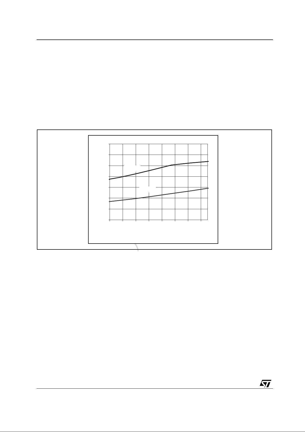
9. OUTPUT DRIVERS
The two output drivers have a high current capability, being able to source up to 2A and to s ink up to
3.5A peak current. Consequently, the two mosfet are switched very quickly, allowing paralleling of
several mosfets to reduce conduction losses. The high level driving voltage is equal to Vcc voltage;
therefore the device drives properly logic level mosfets.
Figure 18: Rds(on) -sink/source vs Temp
1.4
1.4
1.2
1.2
1
1
]
]
Ω
Ω
0.8
0.8
Source
Source
0.6
0.6
Rds on [
Rds on [
0.4
0.4
0.2
0.2
0
0
-40 -20 0 20 40 60 80 100
-40 -20 0 20 40 60 80 100
Sink
Sink
T [ °C]
T [ °C]
10. TRANSIENT BEHAVIOUR
During very heavy load changes, the duty cycle can vary very fast from a low value to a high value and
vice versa in a few switching periods.
The calculation to turn off OUTGate1 is based on On-t ime, so if the on time is changing very fast, the
anticipation time cannot be provided. In any case, STSR2P has a safety feature, which turns off
OUTGate1 when the CK input goes low. OUTgate1 will be turned off with a small delay with respect to
the Ck input- 30ns max (Figure 19 b).
If the anticipation time for OUTGate 2 is based on the calculation of the switching perio d (frequenc y) and
not on duty cycle, even during fast duty cycle changes the anticipation time is provided correctly, always
providing correct driving for the Synchronous Mosfet (Figure 19 c).
14/22

Obsolete Product(s) - Obsolete Product(s)
Figure 19a: Duty Cycle very fast variation
AN1645 - APPLICATION NOTE
Figure 19b: Duty Cycle very fast variation
15/22

Obsolete Product(s) - Obsolete Product(s)
AN1645 - APPLICATION NOTE
Figure 19c: Duty Cycle very fast variation
Figure 19-a shows the condition in which the duty cycle passes from 50% to 80% to 20% and b ack to
50% in four following c ycles. In figure 19-b a magnification of OUT Gate1 behavior is shown. Turn-off
time has very small delay with respect to the clock input. In figure 19-c a magnification of OUTGate2
behavior is shown. Turn-off time maintains the anticipation time even with very strong duty-cycle
variation assuring correct driving in heavy load transient conditions.
11. DEMOBOARD DESCRIPTION
The schematic of figure 20 presents a test board for the STSR2P. This board replaces forward and
freewheeling diodes in a Forward converter. The board includes all the components needed by the
STSR2P to operate. The board allows us to easily pass from diode rectification to synchronous
rectification in Forward converter applications. The components inside the dotted boxes, can be chos en
to implement different circuit configurations for Synchronization and for Inhibit pin. Table 3 shows a
detailed components selection.
16/22

Obsolete Product(s) - Obsolete Product(s)
Figure 20: Demo board Schematic
AN1645 - APPLICATION NOTE
COMP R4
COMP D2
COMP C5
COMP C7
CON1cCON2
c
FR DRAIN
+5V
COMP R11
COMP R5
OFF
R12
+5V
D3
R7
JP5
FR
Q5
FR
Q1
FR
Q4
Q7
NPN smd
4
5
D4
PWRGND
Ck
INHIBIT
CON3
c
FW DRAIN
C1
D1
FWQ2FW
Vcc
SETANT
Q3
2
6
3
R1
R3
R2
1
8
7
SGLGND
PWRGND
OUTGate1
STSR2
U2
OUTGate2
P
FW
Q6
C4
C6
D6
JP2
R6
JP3
R8
Vin
CON5
3
C2
c
VI
78L05
JP1
+5V
1
Vo
GND
2
JP4
C3
COMP R9
COMP D5
COMP R10
JP6
COMP C8
Table 3: Board Components
Component Note
Supply
C4, C6 Vcc bypass capacitors (typ: 100nF)
U1 Standard voltage regulator to provide 5V supply voltage (SOT89). Omit this
component and close jumper JP 1 if +5V is availab le ex t er nally.
C2 78L05 input capacitor (typ: 330nF)
C3 78L05 output capacitor (typ: 100nF)
D6 Zener diode 5.6V
JP1 Close this jumper if a +5V is is available externally
17/22

Obsolete Product(s) - Obsolete Product(s)
AN1645 - APPLICATION NOTE
Synchronization
Q7 Npn Transistor to turn of f t he device
R12 Base resistor for Q2
Comp D2 Small signal di ode:
Comp C5 Capa ci tor:
Comp R5 Resi stor:
Comp R4 Resi stor:
Comp R11 Not mounted Not mounted
INHIBIT
R7
JP5 Clos e t o ope rat e i n di sc o ntinuous m od e condition
JP6 Clos e t o provi de co nst an t negative voltage to Inhibi t
Bla nking Time (Fig.12) Di sabli ng (Fi g.14)
Comp C7
Comp D5
Re sistor Di vi d er (Fi g .6) Pull-up resistor (Fig. 7)
Resistor:
protects Ck pin from voltages
higher than Vc c
to acts like an RC filter to
eliminate the turn-off voltage
spike
low s i de partit i on resist or
high s i de partition res i st o r
Limi ts t he current flowi ng i nto I NHIBI T pin when FW Drain voltage i s hi gher
than V cc
Capac it or :
Provides the negative voltage to
determi ne the bl anking voltage
Resistor:
toget her wi t h C7 det erm in es t he
ti me and volt age value of th e
blank i ng circuit
Pull-up resistor
Not mounted
Not mounted
Diode:
s m al l signal di ode puts Ck pin to l ow l evel
whe n fre e-wheel i ng F ET is conduc ting
Sm al l signal d i ode:
blocks the positive voltage on Inhibit pin
Not mounted
Diod e + res i st or i n series:
Comp R9
Comp R10 Not mounted Not mounted
Comp C8 Not m oun ted
Anticipation
R6, R8 Res i st or divider w hi ch pr ovides volt age level t o set A nt i cipation tim e
JP4 Set s t he m axi m um anticip at i on tim e
JP3 Sets the medium a nticipation time
JP2 Set s t he m i n i m um anticip at ion ti m e
18/22
diode block s t he positive voltage;
resi stor adds the ne gative voltage
to t he Inhibi t pi n
Resistor:
Set t he tim e constant t o charge c apaci tor
C8
Capac it or:
Fi l t er capac i tor t o keep c o nst ant the
volt age on In hi bi t

Obsolete Product(s) - Obsolete Product(s)
AN1645 - APPLICATION NOTE
Pow e r Section
Q1-Q5-Q4 Forward Synchronous Mosfets
Q2-Q3-Q6 Freewheeling Synchronous Mosfet
R2, R3 Gate pull do wn res istors
D1 A Schottky Rectifier in parallel to freewheeling mos fet can increase converter
efficienc y
C1, R1 A s nubbe r reduces f re ew he eling tu rn-o ff spik e
12. BOARD LAYOUT
Any Switch Mode Power Supply requires a good PC B (Printed Circuit Board) design layout in order to
achieve maximum performance in terms of system functionality and emitted radiations. Components
placing, traces routing and width are the major issues.
Some fundamental rules will be given so that the PCB designer can produce a good layout.
All traces carrying current should be drawn on the PCB as short and thick as possible. This should be done
to minimize resistive and inductive parasitic effects, gaining in system efficiency and radiated emissions.
Current return routing is another crucial issue. Signal ground (SGLGND) and power ground (PWRGND)
must be routed separately and connected to a single ground point.
The INHIBIT pin, due to the -25mV comparator could be sensitive to layout, so make the INHIBIT
connection as short as possible.
As a rule of thumb, traces carrying signal currents should be placed far from traces carrying pulsed
currents or quickly swinging voltages avoiding any coupling effect between them.
Figure 21a: Board Layout - Top Components
19/22

Obsolete Product(s) - Obsolete Product(s)
AN1645 - APPLICATION NOTE
Figure 21b: Board Layout - Top Tracks
Figure 21c: Board Layout - Bottom Components
20/22

Obsolete Product(s) - Obsolete Product(s)
Figure 21d: Board Layout - Bottom Tracks
AN1645 - APPLICATION NOTE
13. HOW TO USE THE BOARD
The demo board is meant to implement synchronous rectification in a Forward converter. If diodes are
mounted on the board, they must be removed. Connect the Demo Board as depicted in figure 22. If Vout
is equal or higher than 5V connect Vsupply to Vout (as in the figure). If Vout is lower than 5V, connect
Vsupply together with FW Drain. This last configuration is preferable because, even duri ng short circuit
conditions, the device drives the two mosfets avoiding body diode conduction and consequently
excessive power dissipation.
Figure 22: Connecting the Board to a Forward Converter
FW Drain
FW Drain
Feedback
Vin
Vin
Feedback
Loop
Loop
TRANSFORMER
TRANSFORMER
SCHOTTKY
SCHOTTKY
INDUCTOR
INDUCTOR
SCHOTTKY
SCHOTTKY
Cout
Cout
Vsupply
Vsupply
Vout
Vout
SGLGND
SGLGND
PWM
PWM
FR Drain
FR Drain
PWRGND
PWRGND
21/22

Obsolete Product(s) - Obsolete Product(s)
AN1645 - APPLICATION NOTE
15. CONCLUSION
A new device for controlling synchronous rectifiers in high efficiency AC/DC and DC/DC Forward
Converters is presented. The device is completely transparent to the primary PWM controller, and it
works in the seco ndary side requiring no interaction with the primary side. The dev ice is ab le to operate
with any kind of topological configuration providing the correct driving signal for the two MOSFETs.
The presented board allows implementation of synchronous rectification in any existing forward
converter in an easy and effective way.
Information furnished is believed to be accurate and reliable. However, STMicroelectronics assumes no responsibility for
the consequences of use of such information nor for any infringement of patents or other rights of third parties which may
result from its use. No license is granted by implication or otherwise under any patent or patent rights of
STMicroelectr onics. Spe cifications mentione d in this publication are subj ect to cha nge witho ut notice. This pub lication
supersedes and replaces all information previously supplied. STMicroelectronics products are not authorized for use as
critical components in life support devices or systems without express written approval of STMicroelectronics.
The ST logo is a registered trademark of STMicroelectronics.
All other names are the property of their respective owners
© 2003 STMicroelectronics - Printed in Italy - All rights reserved
STMicroelectronics GROUP OF COMPANIES
Australia - Belgium - Brazil - Canada - China - Czech Republic - Finland - France - Germany - Hong Kong - India - Israel
- Italy - Japan - Malaysia - Malta - Morocco - Singapore - Spain - Sweden - Switzerland - United Kingdom - United States
http://www.st.com
22/22
 Loading...