

Page 1

AN1636
APPLICATION NOTE
UNDERSTANDING AND MINIMISING ADC CONVERSION
ERRORS
By Microcontroller Division Applications
1 INTRODUCTION
The purpose of this do cum ent is to ex plai n th e diffe rent ADC e rrors an d t he tech niques tha t
application developers can use to minimise them. The ADC (Analog to Di gital Converter) is an
important peripheral that connects the analog world to the digital world of microcontrollers.
In this application note the ADC embedded in the ST7 microcontroller is used as an example,
however the same principles to apply to other ADCs.
The accuracy of analog to digital conversion has an impact on overall system quality and efficiency. To be able to improve accuracy you need to understand the err ors associated with the
ADC and the parameters affecting them.
The ADC itself, cannot ensure the accuracy of results, It depends on your overall system design. For this reason, you need to do some careful pr eparation befor e starting your dev elopment.
Lots of parameters affect the ADC accuracy depending on the application. Some of these factors are: PCB layout, voltage source, I/O switching and analog source impedance.
AN1636/0603 1/42
1
Page 2

UNDERSTANDING AND MINIMISING ADC CONVERSION ERRORS
1 INTRODUCTION . . . . . . . . . . . . . . . . . . . . . . . . . . . . . . . . . . . . . . . . . . . . . . . . . 1
1 WHAT IS AN ADC? . . . . . . . . . . . . . . . . . . . . . . . . . . . . . . . . . . . . . . . . . . . . . . 4
2 ADC BLOCK DESCRIPTION . . . . . . . . . . . . . . . . . . . . . . . . . . . . . . . . . . . . . . . 6
2.1 ANALOG INPUT PINS . . . . . . . . . . . . . . . . . . . . . . . . . . . . . . . . . . . . . . . . 6
2.2 ANALOG MULTIPLEXER . . . . . . . . . . . . . . . . . . . . . . . . . . . . . . . . . . . . . 8
2.3 SAMPLE AND HOLD CIRCUIT . . . . . . . . . . . . . . . . . . . . . . . . . . . . . . . . . 9
2.4 CONTROL BLOCK . . . . . . . . . . . . . . . . . . . . . . . . . . . . . . . . . . . . . . . . . 11
2.5 ANALOG SUPPLY AND REFERENCE . . . . . . . . . . . . . . . . . . . . . . . . . . 11
3 ADC TERMIN OLOGY . . . . . . . . . . . . . . . . . . . . . . . . . . . . . . . . . . . . . . . . . . . . 12
3.1 REF ERENCE VOLTAGE . . . . . . . . . . . . . . . . . . . . . . . . . . . . . . . . . . . . . 12
3.2 RESOLUTION . . . . . . . . . . . . . . . . . . . . . . . . . . . . . . . . . . . . . . . . . . . . . 12
3.3 QUANTIZATION . . . . . . . . . . . . . . . . . . . . . . . . . . . . . . . . . . . . . . . . . . . . 13
3.4 MONOTONICITY . . . . . . . . . . . . . . . . . . . . . . . . . . . . . . . . . . . . . . . . . . . 14
3.5 BIPOLAR AND UNIPOLAR ADC INPUT . . . . . . . . . . . . . . . . . . . . . . . . . 14
3.6 HARDWARE AVERAGING . . . . . . . . . . . . . . . . . . . . . . . . . . . . . . . . . . . 15
3.7 SAMPLING THEOR EM . . . . . . . . . . . . . . . . . . . . . . . . . . . . . . . . . . . . . . 15
4 SOURCES OF ER ROR . . . . . . . . . . . . . . . . . . . . . . . . . . . . . . . . . . . . . . . . . . . 16
4.1 POWER SUPPLY NOISE . . . . . . . . . . . . . . . . . . . . . . . . . . . . . . . . . . . . . 16
4.2 POWER SUPPLY REGULATION . . . . . . . . . . . . . . . . . . . . . . . . . . . . . . 17
4.3 ANALOG INPUT SIGNAL NOISE . . . . . . . . . . . . . . . . . . . . . . . . . . . . . . 18
4.4 EFFECT OF ANALOG SOURCE RESISTANCE . . . . . . . . . . . . . . . . . . . 19
4.5 EFFECT OF SOURCE CAPACITANCE . . . . . . . . . . . . . . . . . . . . . . . . . 20
4.6 EFFECT OF INJECTION CURRENT . . . . . . . . . . . . . . . . . . . . . . . . . . . . 24
4.7 I/O PIN CROSS-TALK . . . . . . . . . . . . . . . . . . . . . . . . . . . . . . . . . . . . . . . 25
4.8 EMI-INDUCED NOISE . . . . . . . . . . . . . . . . . . . . . . . . . . . . . . . . . . . . . . . 26
2/42
2
Page 3

UNDERSTANDING AND MINIMISING ADC CONVERSION ERRORS
5 DIFFERENT TYPES OF A/D CONVERTER ERRORS . . . . . . . . . . . . . . . . . . 27
5.1 OFF SET ERROR . . . . . . . . . . . . . . . . . . . . . . . . . . . . . . . . . . . . . . . . . . . 28
5.2 GAIN ERROR . . . . . . . . . . . . . . . . . . . . . . . . . . . . . . . . . . . . . . . . . . . . . . 29
5.3 DIF FERENTIAL LINEARITY ERROR . . . . . . . . . . . . . . . . . . . . . . . . . . . 30
5.4 INT EGRAL LINEARITY ERROR . . . . . . . . . . . . . . . . . . . . . . . . . . . . . . . 32
5.5 TOTAL UNADJUSTED ERROR . . . . . . . . . . . . . . . . . . . . . . . . . . . . . . . 33
6 PCB LAYOUT RECOMMENDATIONS . . . . . . . . . . . . . . . . . . . . . . . . . . . . . . 34
7 HOW POWER SAVING MODES AFFECT THE ADC . . . . . . . . . . . . . . . . . . . 39
8 RELATED DOCUMENTATION . . . . . . . . . . . . . . . . . . . . . . . . . . . . . . . . . . . . 41
3/42
1
Page 4
UNDERSTANDING AND MINIMISING ADC CONVERSION ERRORS
1 WHAT IS AN ADC?
An analog to digital converter is a peripheral whi ch converts analog signal s in a defined range
to the digital outputs.
In the real world, signals are mostly available in analog form. To use a microcontroller in this
type of system, an ADC is required, so that the signals can be converted to the digital values.
The application s oftwa re c an t hen pr ocess th e di gital ou tputs and t ake deci sions de pending
on the application or system requirements.
The limitation imposed by the finite number of digital outputs decides how close the output is
to the analog input. The more bits there are in the output, the closer the digital result will be to
the analog signal. In other words, the resolution of the ADC is defined by the number of bits in
the digital result (8 bits, 10 bits etc) and the input voltage range.
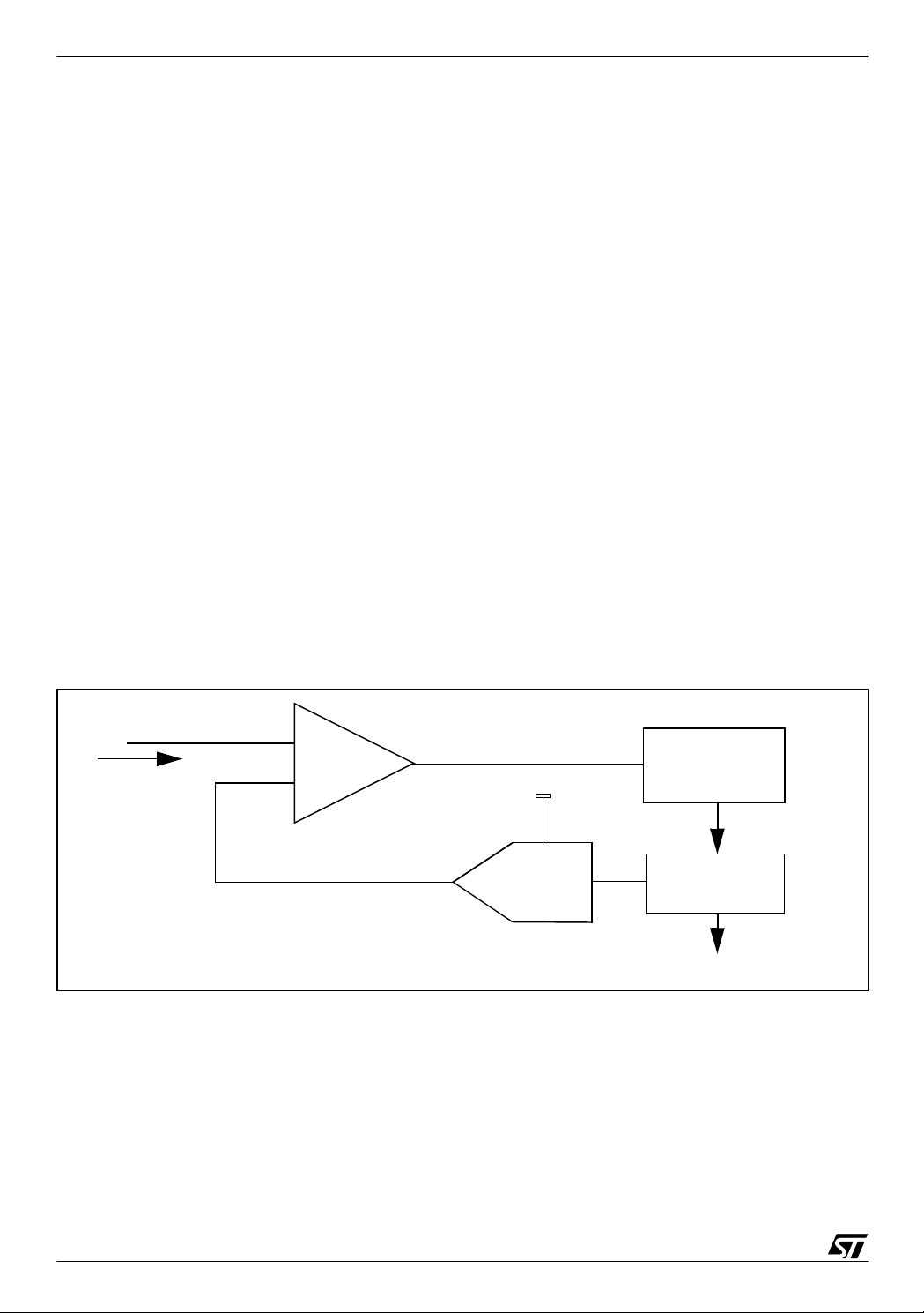
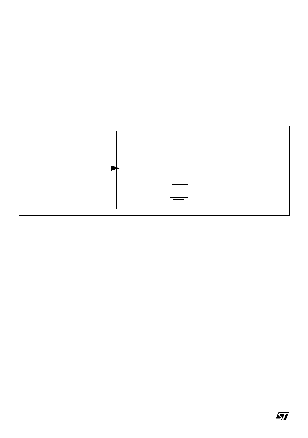
Successive Approximation Method
Different techniques are available for converting analog signal s to digital outputs. The Successive approximation method is the most popular technique. It is also known as Successive approximation Register (SAR) technique. This technique uses binary search method. It consists
of a high speed comparator, DAC (digital to analog converter), and control logic. Refer to
Figure 1.
Figure 1. Successive Approximation Block Diagram
V
IN
+
Control
From Sample
and Hold
Comparator
DAC
V
AREF
Logic
n bit register
Digital Output
The SAR starts by forcing the MSB (Most Significant bit) high (for example in an 8 bit ADC it
becomes 1000 0000), the D AC converts it to V
input voltage with V
/2. If the input voltage is greater than the voltage corresponding to the
AREF
/2. The analog comparator compares the
AREF
MSB, the bit is left set, otherwise it is reset.
4/42
Page 5
UNDERSTANDING AND MINIMISING ADC CONVERSION ERRORS
V
is the reference voltage used by ADC for conversions. The details are mentioned in
AREF
Section 2.5
After this compa rison is done, th e next signifi cant bit is set (=V
/4) and a comparison is
AREF
done again with the input voltage. The procedure is followed till all the bit positions are compared.
At the end of a ll th e bi t c o mp aris on s w e get the cor resp on di ng d i gita l o ut pu t for the a na log
input.
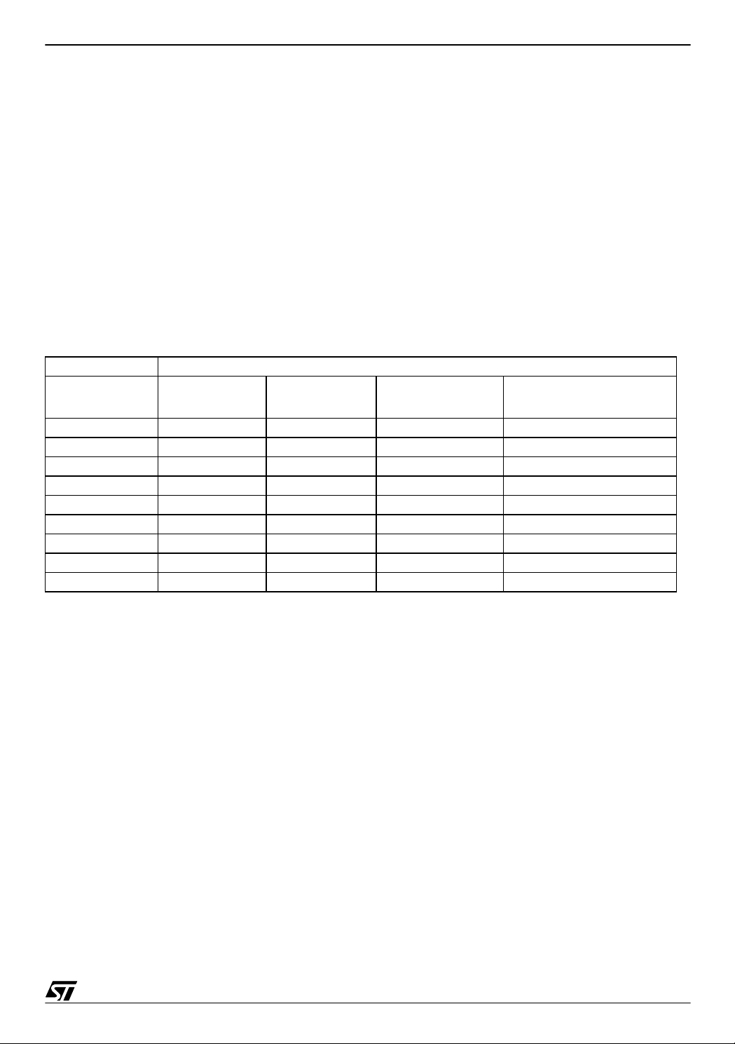
The successive approximation steps are shown in T able 1. As you can see, the digital output
obtained from the ADC is B2h when the analog input is 3.5V.
Table 1. 8-bit ADC successive approximation steps
Steps Vin = 3.5v, V
Digital code DAC output
1 1000 0000 2.5v 1 1000 0000
2 1100 0000 3.76v 0 1000 0000
3 1010 0000 3.13v 1 1010 0000
4 1011 0000 3.45 1 1011 0000
5 1011 1000 3.6 0 1011 0000
6 1011 0100 3.52 0 1011 0000
7 1011 0010 3.49 1 1011 0010
8 1011 0011 3.509 0 1011 0010
Comparator
AREF
output
= 5V
digital out put
(for steps)
Final output = B2h
5/42
Page 6
UNDERSTANDING AND MINIMISING ADC CONVERSION ERRORS
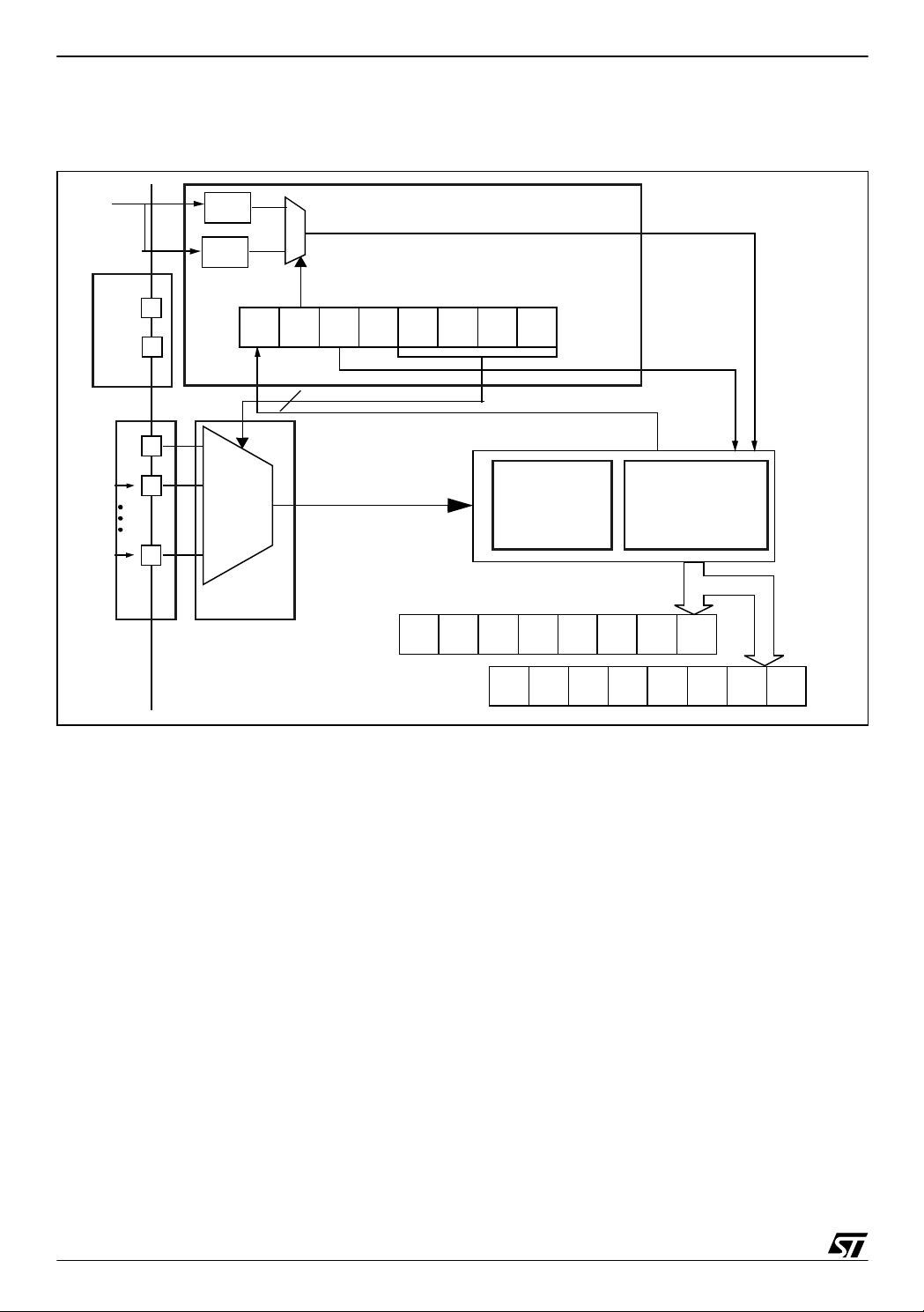
2 ADC BLOCK DESCRIPTION
Figure 2. ADC Block diagram
f
CPU
AIN0
V
V
(f)
AREF
SSA
DIV 4
DIV 2
0
f
ADC
1
CH3
CH2 CH1EOC SPEED ADON 0 CH0
4
(e)
ADCCSR
AIN1
ANALOG
MUX
AINx
(a) (b)
ADCDRH
ADCDRL
The ADC can be divided into the following blocks.
a. Analog input pins
b. Analog multiplexer
c. Sample and Hold circuit
d. Successive approximation block
e. Control block
Sample and
Hold circuit
(c)
000000
Successive
Approximation
Block
D4 D3D5D9 D8 D7 D6 D2
(d)
D1 D0
f. Analog supply/ reference
2.1 ANALOG INPUT PINS
Several analog input pins are ava ilable to connect different analog signals. These are internally multiplexed to use same sample and hold circuit and SAR logic.
6/42
Page 7
UNDERSTANDING AND MINIMISING ADC CONVERSION ERRORS
Figure 3. Electrical diagram of typical ADC ap plication
V
DD
V
T
R
V
AIN
AIN
AINx
C
AIN
0.6V
V
T
0.6V
R
ADC
I
L
±1µA
10-Bit A/D
Conversion
C
ADC
Configuring the analog pin
Choose any I/O port that has analog input c apability (AIN alternate function) and configure it
as floating input. You can do this by writing ‘0’ in the DDR and OR register bits of the corresponding port. At reset, most of the ST7 IOs are configured by default as floating input.
The pin shou ld NO T b e c onfig ured as f loati ng input wi th pul l-up. Th is con figur ation redu ce s
the ADC accuracy. The reason being the potential divider formed between the pull-up resistance and R
from th e V
where R
AIN
. Also some current flows from VDD to the analog source. This current is drawn
ADC
supply. Also there is a potential divider formed between VDD, RPU and R
DD
is the series impedance of the voltage source.
AIN,
Figure 4. Analog input with pull-up
NOT RECOMMENDED
V
RPU should not be enabled.
Current
from V
\/\/\/\/\/
V
IN
DD
R
AIN
DD
R
PU
\/\/\/\/\/\
\/\/\/\/\/\/
R
ADC
C
ADC
V
(Analog Ground)
SSA
Configuring the analog input as floating input with pull-up ( instead of floating input ) will cause
more current to be drawn from the V
supply.There is also an affect on the acc uracy of the
DD
ADC and the digital output converted by ADC may not be accurate.
7/42
Page 8
UNDERSTANDING AND MINIMISING ADC CONVERSION ERRORS
Analo g Pin In put Impedanc e
R
ADC
and C
(hold capacitor) define the input impedance of the analog pins. R
ADC
ADC
is also
called as Rss (Resis tance of samp ling switch an d internal trace /resista nce). Please r efer to
the Sample and Hold circuit explanation in Section 2.3.
If the hold capacitor is fully di scharged, the minimum input impedance is R
. As the hold ca-
ADC
pacitor starts to charge, the curre nt flowing into the pin w ill reduce. If the hold cap acitor is
charge d to a lev el equ al to the ext ernal v oltage there will b e only minima l char ging curre nt
flowing into the analog input.
Figure 5. Analog input pin Impedance
R
ADC
\/\/\/\/\/\/
Input
C
impedance
Zi = R
ADC
+ C
ADC
The minimum input impedance of the analog pin is thus R
value o f R
is specified instead of a typical value, so that the user can calculate the affect
ADC
ADC
V
(Analog Ground)
SSA
. In the datasheet the maximum
ADC
of external resistance on sampling. This is explained in Section 4.4.
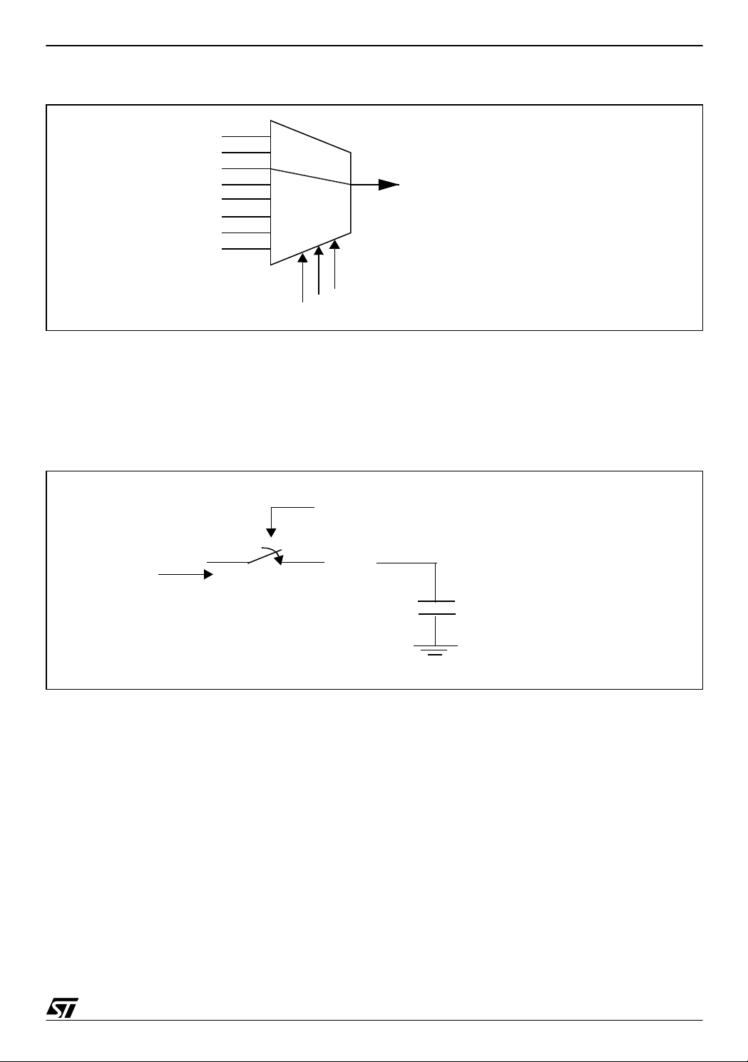
2.2 ANALOG MULTIPLEXER
The ADC can have several analog input pins. These pins are connected internally to the Analog to Digital converter using the analog multiplexer. You can select each pin simply by
writing in the appropriate control register. This allows a single Sample and Hold circuit and Analog to Digital Converter block to be used to convert several analog input sources.
This allows you to switch the analog channels and convert them one by one through software
control.
8/42
Page 9
UNDERSTANDING AND MINIMISING ADC CONVERSION ERRORS
Figure 6. Analog multiplexer
AIN0
AIN1
AIN2
To Sample and Hold
Circuit
Analog Input
AIN7
Channels
Channel selection bits = 010 selects
AIN2
CH[2:0] = 010
2.3 SAMPLE AND HOLD CIRCUIT
The sample and hold circuit samples the input signal and charges the internal hold capacitor
to the voltage equal to V
C
ADC
through R
IN
. The analog pin is then disconnected and the
ADC
voltage across the capacitor is then converted to digital code using successive approximation.
Figure 7. Sample and Hold circuit
Electrically operated
switch
V
IN
R
ADC
\/\/\/\/\/\/
From Analog
Multiplexer
C
ADC
V
(Analog Ground)
SSA
The sa mpl e and hol d ci rcuit cons ists of an e lectr ically ope rated ana log s witc h, in terna l
charging resistance and hold capacitor.
As soon as the ADC c onversion s tarts, the ele ctrically operated switch i s closed, connect ing
the hold capacitor to the analog input through the internal ADC resistance R
. This causes
ADC
a charging current to flow into the analog input and the capacitor starts to charge. The time the
switch remains closed is decided by the f
generally indicated in the datasheet as a multiple of f
Time period t
AD
= 1/f
ADC
. It is called sampling time. The sampling time is
ADC
clock periods.
ADC
9/42
Page 10
UNDERSTANDING AND MINIMISING ADC CONVERSION ERRORS
Figure 8. Sample and Hold timing and electrical diagram
Sampling
Time
tAD = 1/f
Sampling
V
IN
Charging
+ leakage current
Hold and Conversion
Conversion time
ADC
Electrically operated
Switch = Closed
R
ADC
\/\/\/\/\/\/
Electrically operated
Switch = Open
V
C
ADC
SSA
Hold Time
Vc
Capacitor
charged=V
Vc = Voltage developed
across capacitor.
Vc = V
IN
time
Sampling
IN
time
V
IN
\/\/\/\/\/\/
Leakage
R
ADC
C
SAR
ADC
Current
V
SSA
Note: Please refer to product datasheet for Sample and Hold timing for AD C.
SAR = Successive Approximation Register block.
After the sam pling time, the input capacitor has the same voltage as the input, the analog
switch is then di sconn ected f rom the inp ut an d succ essive appro ximation conver sion i s
started, to convert the voltage stored in the hold capacitor. This time is known as Hold time.
It is also expressed in multiples of t
AD
(1/f
ADC
).
The total conversion time of the ADC is the addition of sampling time and hold time. The
sample and hold circuit is also known as track and hold.
10/42
Page 11
UNDERSTANDING AND MINIMISING ADC CONVERSION ERRORS
2.4 CONTROL BLOCK
This block consists of logic which controls the sample and hold circuit, starts the SAR and then
generates the conversion of the ‘conversion complete’ signal for the microcontroller.
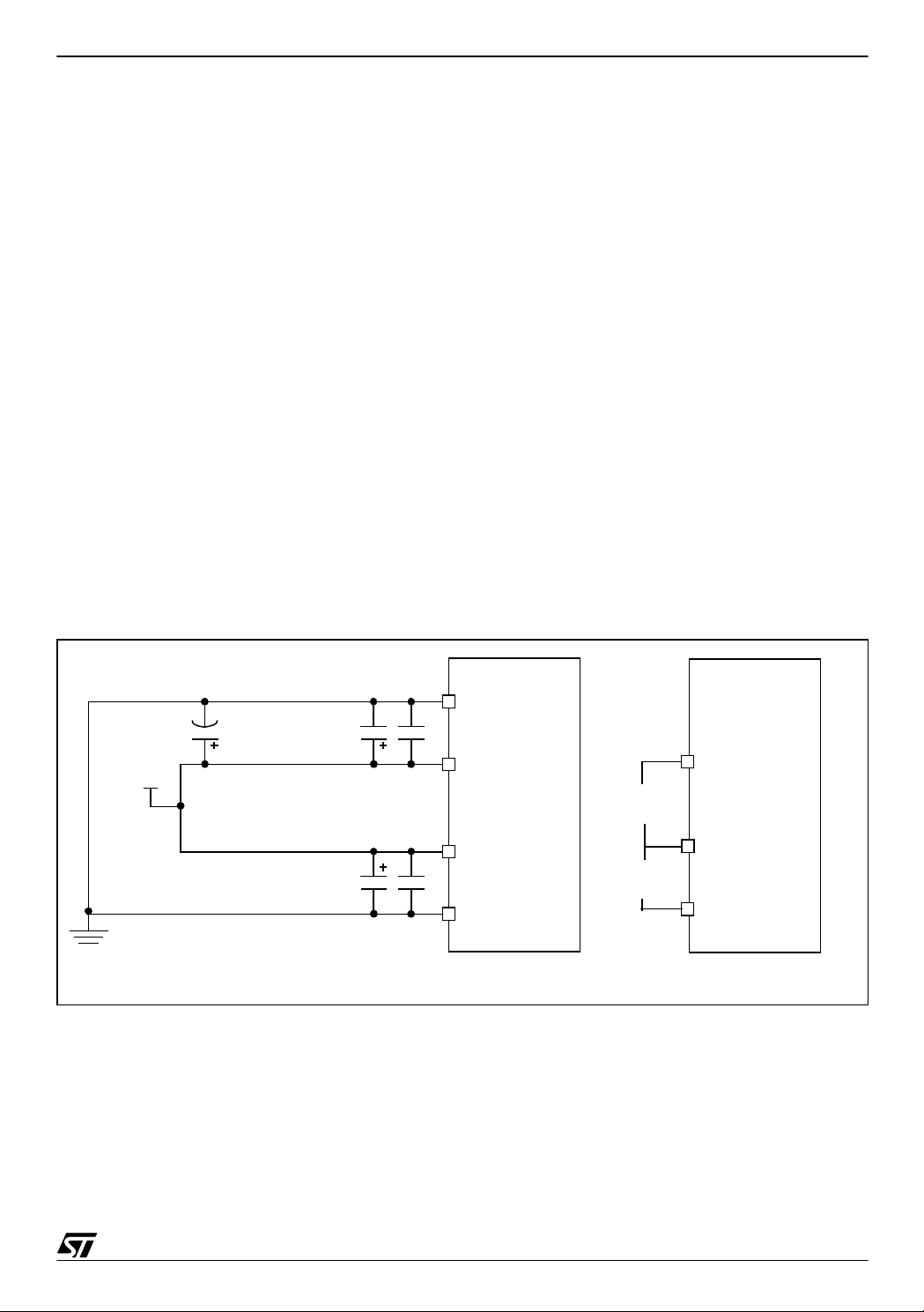
2.5 ANALOG SUPPLY AND REFERENCE
Depending on microcontroller and packaging, the anal og supply pins are g enerally available
on the package.
- analog supply ( or, V
V
DDA
- analog ground.
V
SSA
If these pins are not available the V
to V
internally.
SS
- reference voltage)
AREF
(analog supply) is shorted to VDD and V
DDA
is shorted
SSA
Separate analog power supply pins are available to the user to improve the ADC performance.
It is recommended to put the filtering capacitor between V
noise ( or ripples) on V
The V
from the V
pins are available instead of V
AREF
. You may choose to keep V
DD
are filtered and do not affect the ADC accuracy.
DDA
when the analog supply voltage can be different
DDA
shorted to VDD if a dual supply is to be avoided.
AREF
DDA
and V
so that power supply
SSA
Figure 9. Analog Supply block
V
DD
POWER
SUPPLY
SOURCE
1 to 10µF
ST7
DIGITAL NOISE
FILTERING
(if neede d)
(if ne eded)
EXTERNAL
NOISE
FILTERING
10pF
10pF
0.1µF
0.1µF
ST72XXX
V
SS
V
DD
V
DDA
V
SSA
/\/\/\/\/\ /\
/\/\/\/\/ \/\
V
V
V
ST72xx
DD
AREF
SSA
NOT RECOMMENDEDRECOMMENDED
As these pins provide power supply to the analog block, you should not connect a resistor in
series with V
. This will cause the voltage to drop due to the current flowing through the re-
AREF
sistor and hence will affect the accuracy of the ADC.
Do not leave th e V
DDA/VAREF
ADC, you mu st connect these pins as follows: V
, VSS pins unconnected. If your application does not use the
must be connected to V
DDA
DD,
and V
SSA
11/42
Page 12
UNDERSTANDING AND MINIMISING ADC CONVERSION ERRORS
must be connected to the VSS of the microcontroller. V
V
.
SS
Make sure that V
Similarly V
should not be less than or greater than VSS. There are protection diodes con-
SSA
nected back-to-back between V
is not greater than VDD. There is a protection diode from V
AREF
and VSS.
SSA
cannot have any voltage other than
SSA
AREF
to VDD.
Figure 10. Multisupply Configuration
V
DD
V
AREF
V
SS
BACK TO BACK DIODE
V
SSA
BETWEEN GROUNDS
V
AREF
V
SSA
3 ADC TERMI NO L OGY
There are some terms associated with the ADC which we should understand before we move
further.
3.1 REFERENCE VOLTAGE
The ADC requires a reference voltage to which the analog input is compared to p roduce the
digital output. The digital outpu t is the ratio of the analog i nput w ith respec t to this reference
voltage.
n
digital value =((Analog input voltage)/(reference voltage high- reference voltage low)) * (2
-1)
where n = number of bits of ADC digital output.
The reference voltage is the maximum input voltage that can be converted by the ADC. V
is the reference voltage for the ADC. If V
For example: for 10-bit ADC, V
=1V, V
IN
is not available V
AREF
=5V,
AREF
is used as reference.
DDA
AREF
Digital value = (1V/5V ) *1023 = 204d = 0CCh
3.2 RESOLUTION
The ADC resolution is defined as the smallest incremental voltage that can be recognized and
hence it causes a chang e in the digita l output. It is usual ly expresse d as the numb er of bits
output by the ADC.
12/42
Page 13
UNDERSTANDING AND MINIMISING ADC CONVERSION ERRORS
Hence an ADC which converts the analog signal to a 10-bit digital value, has a resolution of 10
bits.
The smallest incremental voltage that can be recognized is expressed in terms of LSB.
1LSB = (V
AREF
- V
SSA
)/2
n
where LSB = Least significant bit.
n = number of bits output by the ADC.
V
V
An ADC which has ‘n’ bit digital output, provides 2
With a 5V reference voltage, the resolution is 5 (volts) /2
= Reference voltage
AREF
= Analog ground
SSA
n
digital values. It includes both 0 and 2n-1.
10
= 5 (volts)/1024 = 4.88 mV.
This means that for a change in 4.88mV analog input the ADC converted digital value w ill
change by 1LSB.
In reality there are 2
-1 steps. So the actual resolution is 1LSB = (V
AREF
- V
)/(2n -1). As in
SSA
n
practice there is very little difference between the two calculated values because ‘n’ is quite a
large number, both definitions are used.
Figure 11. Resolution representation
Digital
Output
3FFh
N+1
N
Resolution
00h
V
AREF
(n+1)
n
V
AREF
V
AREF
Analog
Input
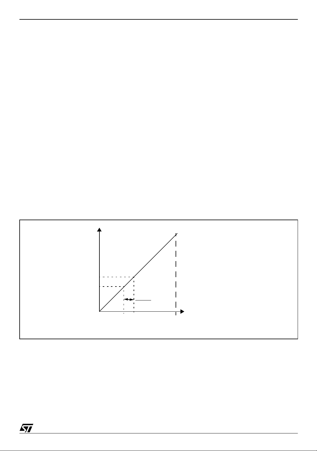
3.3 QUANTIZATION
In theory, the continuous analog signal can be broken into an infinite number of digital steps,
but the quantization of an analog signal by the ADC can be done only in the finite number of
steps which can be produced by the ADC.
13/42
Page 14

UNDERSTANDING AND MINIMISING ADC CONVERSION ERRORS
The quantization error is the error introduced because of the pr ocess of quantization. Ideally
any analog input voltage can be maximum of 1/2 LSB away from its nearest digital code. So
the quantization error is 0.5LSB for the ADC.
Figure 12. Quantization of analog sign al
Step width
1LSB
Digital
output
(Decimal
steps)
Ideal
transfer curve
1
Center of step
= 0 quantization error
V
SSA
1
2
V
IN
Quantization
Error
0.5LSB
0
-0.5LSB
Vin
3.4 MONOTONICITY
Monotoni city is defi ned as a prop erty of the AD C trans fer func tion, which en sures that converted digital values wi ll nev er decrease i f the anal og input does not decreas e and conversion
results will never increase if the analog input does not increase. This property is inherent to the
design of the ADC, subject to the accuracy specified in the datasheet in each case.
3.5 BIPOLAR AND UNIPOLAR ADC INPUT
ADCs that can accept both positive and negative analog signals are known as bipolar.
14/42
Page 15

UNDERSTANDING AND MINIMISING ADC CONVERSION ERRORS
ADCs that can accept only positive input voltage are known as unipolar. ADCs embedd ed in
microcontrollers are unipolar, as the input cannot decrease below the analog ground.
ST7 microcontrollers have unipolar input ADCs and have an input range from 0V to V
AREF
.
In an 8-bit ADC, for example,
– A unipolar ADC with an input range of 0V to 5V will output the digital code 00h for 0V and
FFh for 5V.
– A bipolar ADC with an input range of -5V to +5V will output the digital code 00h for -5V, 80h
for 0V and FFh for +5V.
Figure 13. Bipolar and Unipolar ADC transfer curves
Digital
output
FFh
Digital
Output
FFh
80h
Analog
Input
00h
Bipolar ADC
00h
Unipolar ADC
Analog
Input
transfer curve transfer curve
3.6 HARDWARE AVERAGING
To improve ADC a ccur acy, y ou can pe rform a nu mber of AD C c onvers ions and us e the average of these conversions to obtain more accurate digital output. In hardware averaging
ADCs, this technique is embedded in the hardware and the averaging is done by the hardw are
itself. The final digital output received from ADC is actually the average of the conversions.
This hardwar e ave ragin g tech nique is i mplemen ted in s ome ST7 m icrocontr oller s. T he con version time is thus increased as several conversions are performed.
3.7 SAMPLING THEOREM
The sampling theorem states that to convert the analog signal with frequency ‘f’, the ADC
sampling frequency must be at least twice the anal og signal frequency . So the samp ling frequency must be at least ‘2*f’.
15/42
Page 16

UNDERSTANDING AND MINIMISING ADC CONVERSION ERRORS
Sampling the signal at twice the analog s ignal fr equency wil l not r esult i n a loss of information.
If sampling frequency is less, then the information will be lost. This is a standard theorem that
applies to ADCs in general.
For example: an ADC with a conversion time of 10µs can be used to sample an analog signal
with a time period of 20µs, i.e. 50kHz. (1/20µs).
4 SOURCES OF ERROR
4.1 POWER SUPPLY NOISE
The analog power supply is used as the reference voltage for conversion. As the ADC output
is the ratio between the analog signal voltage and the supply v oltage, any noise on the anal og
reference will cause a change in the converted digital value.
For example: with a 5V supply (analog reference) and 1V signal, the converted result is
(1/5)*1023 = 204d = CCh
But with 40mV ripple peak-to-peak in the power supply, the converted value is
(1/5.04)*1023 = 202d = CAh (when V
was at its peak).
AREF
The SMPS (Switch mode power supply) normally has internal fas t switching power transistors.
This introduces high frequency noise in the output. T he switching noise is in the range of 151Mhz. You can filter this noise by putting low value capacitors (10pf - 22pf) on the power
supply rail. Low value capacit ors have low reactance whereas high val ue capacitors have high
reactance.
Linear regulators have better output in terms of noise. The mains must be stepped down, rectified and filtered and then fed to linear regulators. It is highly recommended to have the filter
capacitors at the rectifier output. Please refer to the datas heet of the linear regulator in each
case. Generally 0.01uF is recommended.
If you are using a switching power supply, it is recommended to have a linear regulator to
supply the analog section.
It is recommended to c onnect capacitors, with good high frequenc y characteri stics, between
the power and ground lines, placing 0.1uF and optionally, if needed 10pF capacitors as close
as possible to the ST7 power supply pins and a 1 to 10uF capacitor close to the power source.
16/42
Page 17

UNDERSTANDING AND MINIMISING ADC CONVERSION ERRORS
Figure 14. Power supply filter ing
ST72XXX
SS
DD
DDA
SSA
V
DD
POWER
SUPPLY
SOURCE
1 to 10µF
ST7
DIGITAL NOISE
FILTERING
(if needed)
(if neede d)
EXTERNAL
NOISE
FILTERING
10pF
10pF
0.1µF
0.1µF
V
V
V
V
The capacito rs allow the AC signal s to pass thr ough them . The sm all value capacito rs filter
high frequency noise and the high value capacitors filter lo w frequency noise. Cer amic capacitors are generally available in small values (1pf to 0.1 µf) and small voltages 16V to 50V. It i s
recommended to place the ceramic capacitors close to the main supply pins (V
analog supply pins (V
DDA
& V
). These filter the noise induced in the PCB tracks. Small ca-
SSA
& VSS and
DD
pacitors can react fast to current surges and discharge quickly for fa st current requirements.
Tantalum capacitors can also be used along with ceramic capacitors.
High value capac itors (1 0µf to 100µ f) wh ich are general ly ele ctroly tic, you ca n use th em to
filter low frequency noise. It is r ecommended to put them near the power source. Y ou c an also
filter high frequency noise using a ferrite inductance in series with the power supply. Ferrites
cause low DC loss (negli gible) unless the c urrent is high. This is because the series resistance
of the wire is very low. But for high frequency, the impedance offered is high.
In most ST7 microcontrollers the V
V
AREF
& V
pins are place d c losed t o e ach other . Th is a llows y ou to put a ca pacito r ver y
SSA
close to the microcontroller with very short leads. For multiple V
& VSS pins are plac ed c lose to eac h oth er. S imila rly
DD
& VSS pins, use separate
DD
decoupling capacitors.
4.2 POWER SUPPLY REGULATION
The power supply should have good line and load regulation. As the ADC uses V
analog reference and the digital value is the ratio of analog input signal and V
AREF
AREF
. So V
as the
AREF
must remain stable at different loads.
Whenever the load is increas ed by switch ing-on a part of the circui t, the increas e in current
must not cause the voltage to decrease. If the voltage remains stable over a wide range of current the power supply has good load regulation.
17/42
Page 18

UNDERSTANDING AND MINIMISING ADC CONVERSION ERRORS
If the voltage decreases, the decrease in V
V
AREF
.
digital output = (V
A change in V
will make a change in the digital output.
AREF
changes the ratio of the analog signal to
AREF
IN/VAREF
) * (2n-1)
For example: for the L7805 voltage r egulator, (Please refer to the L7805 datasheet for details).
Line regulation is 20mV typical for I(load) between 1mA to 100mA.
Similarly, Line regulation is 18mV typical for rectified voltage between 7V to 20V.
4.3 ANALOG INPUT SIGNAL NOISE
The analog signal to be converted may have some noise superimposed on it. There may be a
high frequency noise signal. It is recommended to connect a 10nf capacitor to the analog input
signal. You can also add a low pass filter but this will affect F
, so you should use this only
AIN
if the input signal frequency is low.
is the frequency of the analog input signal. For other details refer to Section 4.5.
F
AIN
18/42
Page 19

UNDERSTANDING AND MINIMISING ADC CONVERSION ERRORS
Figure 15. Noise in analog input signal
10mv Vp-p
~2 LSB
Expected /ideal Signal
at Analog input
V
AIN
Actual Signal
at Analog input
AINx
ADC
10nf
Recommended configuration
with slow input signal
4.4 EFFECT OF ANALOG SOURCE RESISTANCE
The impedance of the analog signal source or series resistance (R
) between source and
AIN
pin will cause a voltage drop across it because of current flowing into the pin.
ADC
and C
The R
When there is R
R
ADC+RAIN
, So the charging time con stant will become (R
form an RC network. The charging of the capacitor is controlled by R
ADC
in series, the effective value of charging of C
AIN
ADC+RAIN
will be governed by
ADC
)*C
. The sampling
ADC
ADC
time for ADC should be greater than 10 times the RC time constant. Please refer to the explanation in Section 4.5.
.
With external input resistance, the sampling time required by the ADC will also increase. The
ADC has a fixed sampling time depending on f
. With the addition of source resistance, the
ADC
time required to fully charge the hold capacitor will increase. If the sampling time is less than
the time required to fully charge the C
ADC
through R
ADC+RAIN,
the digital value converted by
the ADC will be less than the actual value.
Sampling time > 10*(R
ADC+RAIN
)*C
ADC
19/42
Page 20

UNDERSTANDING AND MINIMISING ADC CONVERSION ERRORS
Figure 16. Effect of source impedance on in t e rnal sampling
V
AIN
Vc
R
AIN
\/\/\/\/\/\/
Vc = Voltage across
hold capacitor C
ADC
time
Correct time to charge
to V
C
ADC
IN
Time constant = 10*R
AINx
ADC*CADC
Vc
R
ADC
\/\/\/\/\/\/
C
ADC
V
SSA
(Analog Ground)
V
IN
Increased time to charge
to V
C
ADC
Time constant = 10*(R
IN
AIN+RADC
time
Vc
)*C
ADC
AINx = analog input pin
C
= the hold capacitor of the ADC
ADC
Refer to datasheet for values for R
ADC
and C
ADC
4.5 EFFECT OF SOURCE CAPACITANCE
You have to take the capacitance and resistance at the source i nto account when converting
analog signals
. The source resistance and c apacitance form an RC network and the ADC c on-
version results may not be accurate unless the external capacitor is fully charged to the level
of the input voltage.
The external capacitance at source is denoted by C
20/42
AIN
.
Page 21

UNDERSTANDING AND MINIMISING ADC CONVERSION ERRORS
Figure 17. ADC input wit h R
R
V
AIN
AIN
C
AIN
AIN
, C
Cp
AIN
ST72x
AINx
Cp = Parasitic capacitance
C
= Source capacitance
AIN
The external capacitance will not allow the voltage of the analog input to be exactly the same
as V
analog signal frequency (F
least 10 * R
Figure 18. Recommended R
if it is not fully charged by the analog source. If the analog input signal varies, then the
IN
) should be such that the time period of this analog s ignal is at
AIN
AIN
* C
AIN
.
1000
(Kohm)
AIN
Max. R
100
10
1
AIN
, C
AIN
values
Cain 10 nF
Cain 22 nF
Cain 47 nF
0.1
T
= time period of analog signal = 1/F
AIN
T
F
AIN
AIN
>= 10 * R
= 1/ T
AIN
AIN
* C
AIN
.
<= 1/ (10 * R
AIN
For example:
For R
T
AIN
= 10K, C
AIN
= 10 R
AIN
* C
AIN
AIN
= 10nf
= 10 * 10K* 10n
= 1000µs = 1ms
F
AIN
= 1/T
= 1/1ms = 1KHz maximum.
AIN
0.01 0.1 1 10
f
(KHz)
AIN
AIN
* C
AIN
)
21/42
Page 22

UNDERSTANDING AND MINIMISING ADC CONVERSION ERRORS
Figure 19. Effect of external R and C.
Input
Signal
Signal at analog
input (=across
Cain)
External capacitor not charged to V
The voltage across the capacitor follows the following equation:
Vc = V
(1 - e
IN
)
-t/RC
Vc = Voltage across capacitor
= Voltage from voltage source
V
IN
e = Exponential constant = 2.71 (approx.)
t= Time, after which voltage across the capacitor is to be calculated.
R = Resistance used to charge the capacitor
C= Capacitance value.
R*C = time constant of RC network
Table 2. Voltage across the capacitor
t/RC Vc/V
1 (1- (2.71)
2 (1- (2.71)-2)0.86*V
3 (1- (2.71)-3)0.94*V
4 (1- (2.71)-4)0.98*V
8 (1- (2.71)-8) 0.9996*V
10 (1- (2.71)
IN
-1
)0.63*V
-10
) 0.9999Vin
IN
Vc
IN
IN
IN
IN
IN
It should be noted that when the ratio of t/RC increases, the voltage developed across the capacitor becomes nearly equal to V
. The conversion result will be c orrect only when the ca-
IN
pacitor is fully charged.
Therefore, t >= 10*R*C.
22/42
Page 23

UNDERSTANDING AND MINIMISING ADC CONVERSION ERRORS
The parasitic capacitanc e formed at t he an alog inp ut be cause o f track p aths etc. ap pears in
parallel with external capacitanc e. So it mus t be added to C
capacitance value is much less than C
When C
is small (for example C
AIN
AIN
effectively. So when ADC conversion is started, C
R
ADC
causing C
to effectively discharge. So we need to consider the sampling time re-
AIN
, it can be ignored.
AIN
< 100*C
), it may not be able to hold the VIN voltage
ADC
will appear across the C
ADC
. However when t he paras itic
AIN
through
AIN
quired with external resistance and capacitance.
Figure 20. R
AIN
Vs f
ADC
For example:
With R
=10K, C
AIN
(or Cparasitic) = 10pf, C
AIN
Time for charging external capacitor = R
10*R
AIN*CAIN
= 1us.
ADC
AIN*CAIN
=6pf
= 10k* 10pf = 100ns
Time for charging hold capacitor C
ADC
= (R
AIN+RADC
RC = 12K*6pf =72ns
10RC = 720ns = 0.72us
Total time = 1us + 0.72µs = 1.72µs. (approx.)
So, for ADCs with f
With total time of 1.72µs obtained with R
=2Mhz, sampling time = 4*tAD= 2µs.
ADC
and Cparasitic, the sampling time of 2µs is already
AIN
at its upper limit. If the resistance is higher, f
time. So f
less than 2MHz can be used. It can be noted that for f
ADC
up to 20 kOhm.
)* C
must be decreased to increase the sampling
ADC
ADC
= 1MHz, R
ADC
ADC
can be
23/42
Page 24

UNDERSTANDING AND MINIMISING ADC CONVERSION ERRORS
At lower f
both C
ADC
we can start the ADC conversion as the sampling time is long enough to charge
ADC,
and C
(or Cparasitic).
AIN
4.6 EFFECT OF INJEC TION CURRENT
ST microcontrollers have robust tolerance of additional leakage current introduced on analog
input signals as a n eff ect of negative injecti on curr ent. Negative injectio n curren t on any an alog pin (or closely placed digital input pin) may introduce leakage current into the ADC input.
The worst case is the adjacent analog channel. Negative injection current is introduced when
V
IN<VSS
. Therefore current flows out from the I/O pin.
Analog pi ns ca n be pro tected agai nst neg ative inj ection by adding a Sch ottky diode ( pin to
ground).
For example:
For an injection of 0.8mA on the analog input pin ST specifies a maximum l eakage c u rrent of
1.6µA (please refer to the respective product datasheet)
as Voltage = Current * Resistance. The voltage drop due to this leakage current across R
AIN
is:
AIN
)= R
V (R
If source series resistance R
AIN
* I
Leak
is 10K, the leakage current will introduce 1.6µA*10kohm =
AIN
16mV for 10-bit ADC, 1LSB = 5V/1023 = 4.8mV. A dr op of 16m V will correspond to approximately a drop of 4LSB. This means that all the digital converted values will contain an error of
4LSB. This means that after the ADC converts the input signal, the di gital output will always be
4LSB less than it should be.
24/42
Page 25

UNDERSTANDING AND MINIMISING ADC CONVERSION ERRORS
Figure 21. Effect of injection current
Vain
R
AIN
\/\/\/\/\/\/
Leakage
AIN0
ADC
current
AIN1
VIN < V
SS
injection
current
V
Microcontroller
SSA
This demonstrates that the source impedance should be as small as possible to obtain maximum accuracy. With no negative injection current, no loss of accuracy is expected.
Positive injection current is introduced when V
> VDD. Therefore current flows into the I/O
IN
pin. Positive injection current within the limit does not cause any loss of accuracy.
Minimizing Injection current
Check the application to verify if any digital or analog input voltages can be less than V
. In this case negative injection current will flow from the pins. Negative injection current
V
SSA
SS
or
will have gr eater aff ec t on the accuracy, when a digital input is close to the analog input being
converted.
It is recommended to connect a Schottky diode from V
to the IO which can have the neg-
SSA
ative injection current.
4.7 I/O PIN CROSS-TALK
Switching the I/Os may induce some noise in the analog input of the microcontroller. This is
because of capacitive coupling between the I/Os. The cross-talk may be introduced by PCB
tracks running close to each other or crossing over each other.
Within the microcontroller there can be non-negligible effect on I/Os because of switching etc.
Internally switching digital signals and I/Os introduces high frequency noise. If high sink I/O s
are switched, this may induce some voltage dips in the pow er supply because of the current
surges.
A digital track crossing over an analog input track on the PCB may affect the analog signal.
25/42
Page 26

UNDERSTANDING AND MINIMISING ADC CONVERSION ERRORS
Figure 22. Cross-talk between I/Os
Analog-in
Digital
I/O
Digital and analog
signal passing close
to each other
Analog-in
Digital
I/O
Digital and analog
signal tracks crossing
each other on different
Analog-in
Digital
I/O
Recommended
Grounding between
signals
side of the PCB
Shielding the analog signal by placing ground tracks across it helps reduce noise
produced by cross talk etc.
4.8 EMI-INDUCED NOISE
Electromagnetic emissions from neighboring circuits may introduce high frequency noise into
an analog signal because the PCB tracks may act like an antenna.
You can reduce the emi ssion noise by proper s hielding and layout techniq ues. The pos sible
sources of emissions must be physically separated from the receptors. You can separate
them electrically by proper grounding and shielding.
You can minimize the reception noise by using filtering techniques so that high frequency
noise is filtered.
Figure 23. EMI sources
I/O
Electro-
magnetic
coupled
Noise
Noise
Analog
ADC
Source
Induced
noise from
Internal
Noise
Microcontroller
PCB tracks
26/42
Page 27

UNDERSTANDING AND MINIMISING ADC CONVERSION ERRORS
Shielding
Placing ground tracks alongside sensitive analog signals provides shielding on the PCB. The
other side of the two-layer PCB should also have a ground plane. This prevents interference
and I/O cross-talk affecting the signal.
Signals coming from distant locations (like sensors etc) should be connected to the PCB using
shielded cable. Care should be taken to minimize the length of the paths of these types of
signal on the PCB.
The shield should not be used to c arry the ground referenc e from the s ensor or analog source
to the microc ontroller. A se parate wi re should be used as g round. The shield should be
grounded at only one plac e near the receiver s uch as the anal og ground of the microcontrol ler.
Grounding the shield at both the ends (sour ce and recei ver) may caus e ground lo ops to be
formed and making the current flow from the shield.
Figure 24. Shielding
Not Recommended
Recommended
Sensor Sensor
ADC
Ground
ADC
Currents
Do not ground the
shield at both ends
Grounding the
shield at the receiver end only
If the current is flowing through the shield, it will act like an antenna and the pur pose of
shielding will be lost.
The shielding concept also applies to grounding the chassis of the application if it is metallic.
This also helps to remove EMI and EMC interference. In this case the mains ‘Earth Ground’ is
used to shield the chassis. Similarly DC ground can also be used for shielding in case ‘Earth
Ground’ is not available.
5 DIFFERENT TYPES OF A/D CONVERTER ERRORS
Different error types are specified for A/D Converters. These errors are normally expressed as
multiples of LSB for easy reference. The resolution in terms of voltage depends on the reference voltage. You can calculate the error in terms of voltage by multiplying the (
LSB
) with (
voltage corresponding to 1LSB
).
number of
27/42
Page 28

UNDERSTANDING AND MINIMISING ADC CONVERSION ERRORS
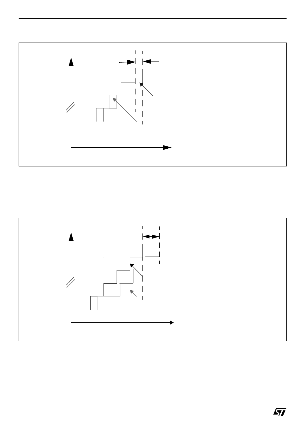
5.1 OFFSET ERROR
This is defined as the deviation between the first actual transition and the first ideal transition.
The first transition is when the digital output of ADC changes from 0 to 1. In an ideal case we
should get a digital output of 1, when the analog input is between 0.5 LSB to 1.5LSB. The first
transition in an ideal case will be at 0.5 LSB. Offset error is represented as E
.
O
Example 1:
In a 10-bit ADC, ideally 2.44mV (0.5 LSB = 0.5 * 4.88mV) input should generate a corresponding digital output of 1. But in practice the ADC may still show the reading as 0. If we get
a digital output of 1 from an analog input of 10mV, then:
Offset error = Actual transition - Ideal transition
= 10mV - 2.44mV = 7.56 mV
E
O
= 7.56mV / 4.88 mV = 1.54 LSB
E
O
When an analog input voltage of greater than 0.5LSB generates the first transition, then the
offset error will be positive.
Figure 25. Positive offset error representation
E
Digital
output
(Decimal
steps)
O
= Offset error (positive)
E
O
Ideal
transfer curve
Actual
transfer curve
1
V
0.5LSB
When the analog input voltage V
IN
= V
and the A DC gener ates a non-z ero digital o utput
SSA
IN
then the offset error will be negative. This will mean that theoretically (or by Extrapolation) a
negative vo lta ge w ill gen erate the fi rst tra ns ition. As spec ified i n th e data sheet , any v olta ge
less than V
will cause the digital output to be 0.
SSA
28/42
Page 29

UNDERSTANDING AND MINIMISING ADC CONVERSION ERRORS
Figure 26. Negative offset error representation
Digital
Output
E
O
Ideal
transfer curve
= Offset error (negative)
E
O
1
0.5LSB
Actual transfer curve
V
IN
5.2 GAIN ERROR
Gain Error is defined as the deviation between the last actual transit ion and the l ast ideal tr ansition. Gain error is represented as E
.
G
The last actual tr ansition m eans the tr ansition from 3F E to 3FF fo r a 10-bit ADC . In an ide al
case we should get a transition from 3FE to 3FF from a 10-bit ADC, when the analog input is
equal to V
-0.5LSB. So for V
AREF
If ADC provides the 3FFh reading for V
= 5V, last ideal transition shall be at 4997.12 mV.
AREF
IN
< V
-0.5LSB, then we have a negative gain error.
AREF
Example
For a 10-bit ADC and V
= 4990 mV generates transition from 3FE to 3FF then,
If V
IN
AREF
=5v
Gain error E
= 4990mV - 4997.12 mV
E
G
= - 7.12 mV
E
G
= (-7.12mV / 4.88mV) LSB = -1.45 LSB
E
G
= Last actual transition - ideal transition
G
29/42
Page 30
UNDERSTANDING AND MINIMISING ADC CONVERSION ERRORS
Figure 27. Negative Gain error representation
E
G
1023
Digital
= Gain error (negative)
output
E
G
(Decimal
steps)
Ideal
transfer curve
Actual
transfer curve
1022.5
V
IN
LSB
If we do not get full s cale r eading ( 3F F for a 10-bi t ADC ) for V
equal to V
IN
will be positive.
This means theoretically (or by extrapol ation), a v oltage greater than V
transition.
Figure 28. Positive Gain error representation
E
G
1023
Digital
= Gain error (positive)
output
E
G
the gain error
AREF
will cause the last
AREF
(Decimal
steps)
Ideal
transfer curve
Actual
transfer curve
1022.5
V
IN
LSB
5.3 DIFFERENTIAL LINEARITY ERROR
Differential Linearity Error (DLE) is defin ed as the maximum deviati on between actual step s
and the ideal steps. Here ‘ideal’ is not for the ideal transfer curve but for the resolution of the
ADC. DLE is represented as E
30/42
D.
Page 31

UNDERSTANDING AND MINIMISING ADC CONVERSION ERRORS
DLE = Actual step width - 1LSB
Ideally analog input voltage change of 1LSB should cause a change in the digital code. If an
analog input voltage greater than 1LSB is required for a change in digital code, then the ADC
has the differential linearity error. DLE thus corresponds to additional maximum voltage that is
required to change one digital code to the next digital code.
DLE is also known as DNL, Differential Non-Linearity error.
Example:
For a range of analog input we should get the same digital output. Ideally the step width should
be 1LSB. Suppose we get same digital output for a range of analog input voltage 1V to 1.010V
then the step width will be 1.010V-1V = 10mV. DLE is thus the voltage di fference between the
higher (1.010V) and lower analog voltage (1V) subtracted by the voltage corresponding to
1LSB.
Figure 29. Differential Error representation
(Negative)
E
D
Digital
output
Positive
1LSB
E
D
Ideal Transfer curve
ideal
(Decimal
steps)
1LSB
= Differential linearity
E
D
error
Actual
transfer curve
1
V
SSA
V
IN
Note: In this example the actual curve is shown to have an offset error from ideal curve.
With a 10-bit ADC and V
= 5V, an ana log input of 1V can provide res ults varying fr om
AREF
CBh to CDh.
Similarly for 1.010V, i.e. 206d = CEh, the results may vary from C Dh to CFh.
So, total voltage range corresponding to the step CDh is 1.010 V - 1V
= 10mV
= 10mV - 4.88 mV
E
D
= 5.12 mV
E
D
31/42
Page 32

UNDERSTANDING AND MINIMISING ADC CONVERSION ERRORS
ED= (5.12mV/4.88mV) LSB
= 1.04 LSB
E
D
Here we assume that any voltage greater than 1.010 V will not result in the digital code equal
to CDh.
When the step width is less than 1LSB, DLE will be negative.
5.4 IN TEGRAL LINEARITY ERROR
Integral Linearity Error is maximum deviation between any actual transition and the endpoint
correlation line. ILE is represented as E
L.
The endpoi nt corre lation line can be d efined as the lin e on the A/D trans fer curve th at con nects the first actual transition and last actual transition. ILE is the deviation from this line for
each transition. The endpoint correlation line thus c orresponds to the actual transfer c urve and
has no relation to the ideal transfer curve.
ILE is also k nown a s IN L, Integr al Non linearity Erro r. ILE is the i ntegral of DLE ov er the full
range.
Figure 30. Integral error representation
1023
Endpoint correlation
Line
Digital
output
E
L
= Integral linearity error
E
L
(Decimal
steps)
Actual
transfer curve
1
V
SSA
V
IN
Example:
If we get the first transition from 0 to 1 at 10mV ( offset er ror ) and we get the last transition
(3FE to 3FF) at 4.990V (gain error) then the line on transfer curve connecting the actual digital
code 1 and the actual digital code 3FF will be the endpoint correlation line.
32/42
Page 33

UNDERSTANDING AND MINIMISING ADC CONVERSION ERRORS
5.5 TOTAL UNADJUSTED ERROR
TUE is defined as the maximum deviation between the actual and the ideal transfer curves. It
is a parameter which specifies the total errors that can occur causing maximum deviation between the ideal digita l output and a ctual d igital output . It is the m aximum dev iation recor ded
between ideal expected value and actual value obtained from the ADC for any input voltage.
TUE is represented as E
T.
TUE is not the sum o f EO, EG, EL, ED. The offset er ror affects the digital r esult at lower v oltages whereas the gain error affects the digital output for higher voltages.
Example:
With a 10-bit ADC and V
=5V and 1V input, the ideal result i s CCh. But i f on conversion we
AREF
get the result CEh, this deviation may be because of offset, DLE and INL errors occurring simultaneously.
TUE = absolute (actual value - ideal case value).
= CEh - CCh
= 2h
Figure 31. Total unadjusted error
Et
Digital
output
(Decimal
steps)
Ideal
transfer curve
Et = Total Unadjusted error
Actual
transfer curve
1
V
SSA
V
IN
33/42
Page 34

UNDERSTANDING AND MINIMISING ADC CONVERSION ERRORS
Using error parameters
1. The TUE is NOT the sum of all the errors E
, EG, EL, ED. It is the maximum e rror wh ich can
O
occur between ideal and expected digital values. It can be the effect of either a single error
or two errors occuring simultaneously.
2. As ILE is the integral of DLE, i t can be considered as indicative of maximu m error. Do not
add both DLE and ILE together to calculate the maximum error which can occur at any digital step.
3. Integral Linearity Error is the maximum deviation between any actual transition and the end
point correlation line. So it represents the linearity of the ADC.
4. ILE and DLE are dependent on the ADC design. It is difficult to calibrate them.
5. The ILE and DLE can be minimized by doing multiple conversions and then averaging.
6. Offset and Gain errors can be easily cancelled / compensated using software techniques.
7. The maximum values for errors specified in datasheet are the worst error values measured
in the laboratory test environment for full voltage range.
8. As already mentioned, all the ADCs provide the digital converted output in ratio with the ref-
erence voltage. To convert analog voltage accurately, the A DC needs to have an accurate
V
otherwise the digital output received may not be the correct value.
AREF
Example:
In the widely used 7805 voltage regulator, the datasheet (L78M05C) specifies Vo min.= 4.8V
and Vomax = 5.2v. This variation is 0.2V from r equired 5V. Hence a variation of 200mv. With
an analog input of 1V and with V
=5V, the expected digital output should be (1/5)*1023 =
AREF
204d = CCh
But if V
= 4.8v, the digital output = (1/4.8)*1023 = D5h
AREF
So the power supply variation has caused a change of D5-CC = 9.
In this case to measure the true input voltage, all the relevant parameters must be verified and
crosschecked. For example, if a precision voltage regulator such as the L78M05AB is used, it
provides Io=350mA and Vomin=4.9V, Vo max = 5.1V.
6 PCB LAYOUT RECOMMENDATIONS
For best ADC conversion accuracy, you should follow these PCB layout guidelines.
1. Separate the analog and digital layouts
34/42
Page 35

UNDERSTANDING AND MINIMISING ADC CONVERSION ERRORS
It is recom mend ed to s eparat e the an alog an d digital circu itry on t he PCB . They should be
placed in different parts of t he PCB . This a lso av oids tracks crossing each other. The track s
carrying digital signals may introduce high frequency noise in analog signals because of coupling. The digital signals produce high frequency noise because of fast switching.
Coupling of the capacitive nature is formed because of the metal connections (tracks) separated by the dielectric provided by the PCB base (glass, ceramic or plastic).
It is recommended to use different planes for analog and digital ground. If there is a lot of analog circuitry then an analog ground plane is recommended. Analog ground must be placed
below the analog circuitry.
Figure 32. Separating the analog and digital layouts
Power Supply
Analog circuitryDigital
Digital
Ground
Circuitry
(Noisy and noise
Generating)
Micro
Controller
(affected by noise)
Analog
Ground
2. Separate power supplies for analog and digital circuits
It is desirable to have separate analog and digital power supplies in cases where there is a lot
of analog and digital circuits external to the microcontroller. Depending on the microcontroller
package, differe nt analog and digital pow er supply and grou nd pins are availab le. Internally
V
AREF
and V
pins are not connected except for protection through Schottky diodes. These
DD
pins can be powered from separate power supplies.
In low pin-co unt package s, separ ate anal og and dig ital supply and groun d pins may no t be
available. In this case they are internally shorted. So V
and VDD are internally connected
DDA
in packages which have fewer pins.
As mentioned earlier, if you use a switching type power supply for the digital circuitry, you
should use a separate linear supply for the analog circuit.
Also, if you expect a lot of noise on the DC power supply due to I/O switching etc, a separate
supply for the analog section is preferable.
35/42
Page 36

UNDERSTANDING AND MINIMISING ADC CONVERSION ERRORS
Important: Separate Analog and Digital supplies are recommended only if the microcontroller
has V
not have V
pins for the ADC reference voltage (ins tead of V
AREF
pins, then the difference between V
AREF
). If the microc ont roller doe s
DDA
and VDD should not be more than the
DDA
difference specified in the datasheet (check the Absolute maximum ratings). Generally the difference between V
DDA
and V
is specified as 50mV, hence separate supplies are not recom-
DD
mended.
Figure 33. Separating the analog and digital supplies
Analog
Circuit
Linear
Regulator
V
AREF
V
SSA
V
SS
Microcontroller
SMPS
AC
mains
V
DD
36/42
Page 37

UNDERSTANDING AND MINIMISING ADC CONVERSION ERRORS
3. Connect analog and digital power supplies in a star net work
It is recommended to connect the analog and digital grounds in star network. This means that
you must connect the analog and digital grounds onl y at one poi nt. This av oids noi se being i ntroduced in the analog power supply section, because of digital signal switching and also
avoids current surges affecting the analog section.
Figure 34. Star connection for analog and d igital supplies
Digital
Circuit
Analog Circuit
Analog
Ground
Analog
Current
Digital
Current
Digital
Ground
Power Supply
4. Using separate PCB layers for supply and ground
Two-Layer PCBs
For two layer PCBs it is recommended to provide a maximum area for the ground. The power
supply (V
DD
, V
) should run through thick tracks. The ground area between two layers can
DDA
be shorted together via multiple connections in the overlap region if they are same ground signals. The unused area of the PCB can be filled with the ground area.
The other convention is to fill the unused area of PCB on one layer with positive supply (V
DD
and unused area on other plane for Ground. T he advantage is reduced inductance for power
and ground signals. Maximum ground area on PCB provides a good shie lding effect and reduces the electromagnetic induction susceptibility of the circuit.
Multilayer PCBs
)
Wherever possible, try to use multilayered PCBs and use separate layers on the PCB for
power and ground. The V
, VSS pins of the various ICs can be directly connected to the
DD
37/42
Page 38

UNDERSTANDING AND MINIMISING ADC CONVERSION ERRORS
power planes thus reducing the tracks needed to connect the supply and ground. Longer
tracks will have a high inductive effect. T he analog ground can be connected at one point to
this ground plane, this should be near to the power supply.
A full ground plane provides a good s hielding effect and reduc es the Electromagneti c induction susceptibility of the circuit.
Figure 35. Multlayer PCB configuratio ns
1. Top layer and bottom
layer for SMD components
2. Second layer as power
plane
3. Third layer ground layer
There will be tr acks passing vertically through the ground and supply planes.
SMD: Surface mounted devices
1. Top layer and bottom layer
for SMD components
2. Second layer as digital
ground plane.
3. Third layer as analog ground
Digital and analog ground connected
at one point near power supply
1. Top layer and bo ttom layer
for components and ground plane
( Analog and digital )
2. Second and third layer for tracks
The disadvantage of multilayer PCBs is the higher cost of manufacturing and the fact that they
are more difficult to debug.
Single-layer PCBs
Single-layer PCBs are used to save cost. They can be used only in s impl e applications when
the number of connections is very limited. It is recommended to fill the unused area with
ground. Jumpers can be used to connect different parts of the PCB.
5. Component placement and rout ing
Place the components and route the signal traces on the PCB to shield the analog inputs. Analog signal paths should run over the analog ground plane.
Components like resistors and capacitors must be placed with their leads very short. Surface
mounted devices (SMD), resistors and capacitors can be us ed. SMD capacitors can be placed
close to the microcontroller for decoupling.
The tracks for the power should be wide, as the series resistance of these tracks will cause the
voltage drop if the tracks are narrow. Narrow power tracks wil l have non-negligible fi nite resistance. High load current will cause some voltage drop across these tracks.
38/42
Page 39

UNDERSTANDING AND MINIMISING ADC CONVERSION ERRORS
Quartz crystals mus t be surrounded by groun d tracks/plane. Th e other side of the two layer
PCB below the crystal should preferably be covered by the ground plane. Most crystals have
a metallic body that should be grounded. The crystal should be placed close to the microcontroller. Surface mounted crystals are available and can be used.
6. Software considerations
Do not toggle digital outputs on the same I/O port as the A/D input being converted. This will
introduce switching noise into the analog inputs.
Toggling high sink I/Os may introduce high frequency noise in the power supply, this may affect the conversion results.
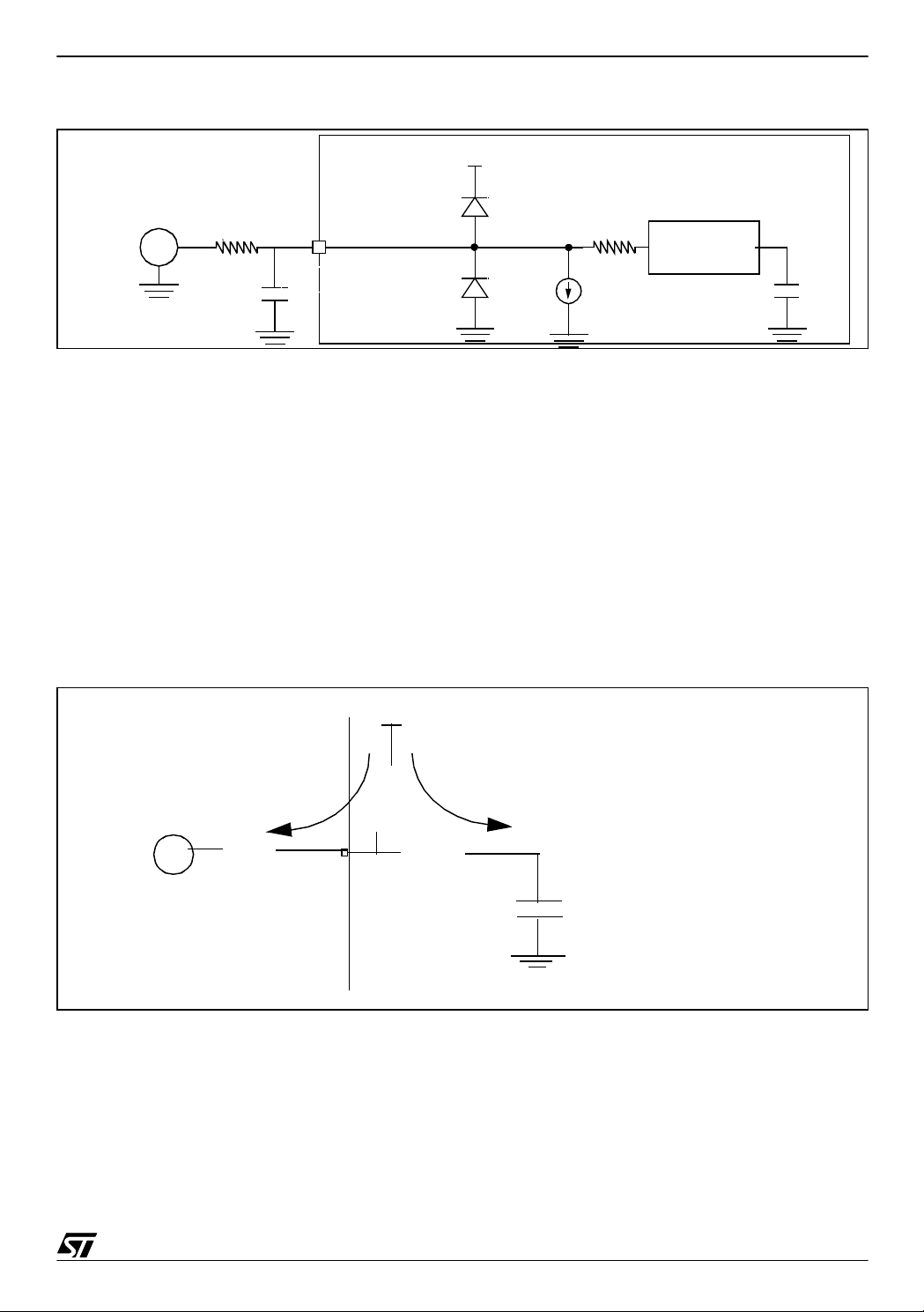
7 HOW POWER SAVING MODES AFFECT THE ADC
Wait mode
ADC can be used when the microcontroller is in Wait mode. You can take advantage of the reduced internal noise in the microcontroller to improve ADC conversion results.
Halt mode
Entering Halt m ode w ill d isable t he A DC, i rrespe ctive of w hether the A D ON bit is set or not.
This is because executing the HALT instruction shuts down the ADC.
Exiting from Halt mode require s some stabilization time b efore ADC conversio n should be
started. This conversion time is very small. Please refer to the datasheets.
Table 3. Summary Table
Oscilla tor /CPU/Peripher a l St a tus
ST7 Modes
Run On On X Reset On
Slow On On X Set On
Wait On Off X Reset On
Slow-Wait On Off X Set On
Oscil-
lator
CPU
MCCSR-
OIE Bit
MCCSR-
SMS Bit
ADC
Use the ADC as mentioned in datasheet.
Take care that f
below f
If ADC has exit-from Wait capability, this mode is recommended.
If ADC has exit-from Wait capability, this mode is recommended.
Effect on ADC
ADC
min.
ADC
does not fall
39/42
Page 40

UNDERSTANDING AND MINIMISING ADC CONVERSION ERRORS
Oscilla tor /CPU/Peripher a l St a tus
ST7 Modes
Active-Halt On Off Set X Off
Halt Off Off Reset X Off
Oscil-
lator
CPU
MCCSR-
OIE Bit
MCCSR-
SMS Bit
ADC
Exit from Halt mode requires stabilization time before conversion
starts.
Exit from Halt mode requires stabilization time before conversion
starts.
Effect on ADC
Note: Reset=0, Set=1
Rules and Recommendations for using the ADC in Power Saving Mode
Different power saving modes for ST7 can be selected depending on pow er saving requirements of the a ppli cation , the f ollow ing rules and reco mm en dati ons sh ould be appl ied wh en
using the ADC.
1. When switching to Slow mode from Run mode care should be taken that the f
fall below the f
minimum specified. Otherwise the conversion results are not guaranteed.
ADC
should not
ADC
Similarly when application switches to Slow-wait mo de after recovering from Wait mode,
f
shall be in specified range.
ADC
2. Similarly, when switching back from Slow mode to Run mode (or Slow-Wait to Wait mode),
if ADC conversion is intended, the f
should not increase above the f
ADC
max specified in
ADC
the data sheet. Conversion results are not guaranteed outside the operating frequency
range of ADC.
3. For ADCs with Wait mode wake up capability, it is recommended to use Wait mode for ADC
conversion. This will improve results because the CPU is off in Wait mode, and this reduces
the noise generated by digital switching.
4. If the ADC doe s not have an inter rupt capabi lity for wakin g up from Wait mode, then any
other interrupt (for example a Timer interrupt) can be used to take advantage of the reduced
intern al noise in W ait mo de. Be fore ent ering Wait mode , ADC convers ion ca n be star ted,
and the results can be read after exit from Wait mode.
5. If ADC is off/disabled, leakage current can flow into the ADC if the analog channels are con-
nected to the analog input pins. This is because of finite impedance of IO pins.
6. If the ADC is not used in the application, and you want to save power consumption, then you
must disable the ADC through software.
7. When entering a power saving mode, disable the ADC if you do not need it to perform con-
version while the microcontroller is in power saving mode. If the ADC is not disabled before
40/42
Page 41

UNDERSTANDING AND MINIMISING ADC CONVERSION ERRORS
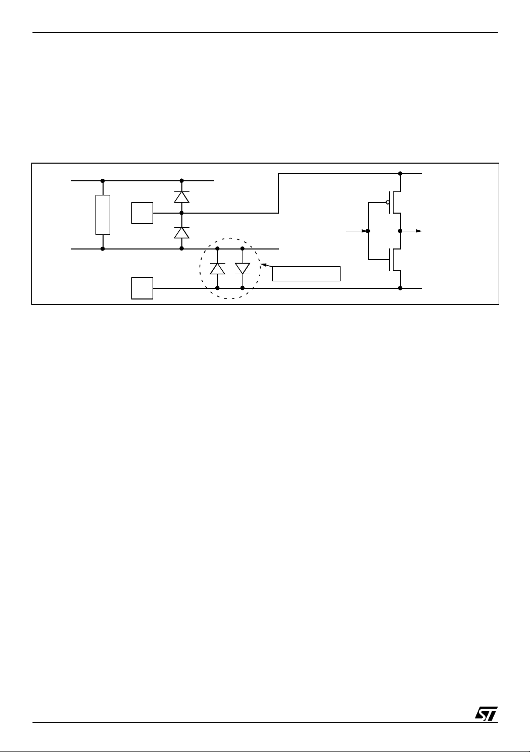
entering power saving mode (except Halt or Active-Halt), the internal analog circuit will consume some current.
8 RELATED DO CUMENTATIO N
You can refer to the following application notes for additional useful information:
AN435: Designing with microcontrollers in noisy environment
AN898: EMC General Information
AN901: EMC Guidelines for microcontroller - based applications
AN1015: Software techniques for improving microcontroller EMC performance
41/42
Page 42

UNDERSTANDING AND MINIMISING ADC CONVERSION ERRORS
THE PRESENT NOTE WHICH IS FOR GUIDANCE ONLY AIMS AT PROVIDING CUSTOMERS WITH INFORMATION
REGARDING THE IR PRO DUCT S IN OR DER FO R THEM TO SAV E TIME . AS A RES ULT, STMIC ROEL ECTR ONI CS
SHALL NOT BE HELD LIABLE FOR ANY DIRECT, INDIRECT OR CONSEQUENTIAL DAMAGES WITH RESPECT TO
ANY CL AIM S AR IS IN G FR OM T HE CO N TENT OF S UC H A NO TE A ND /O R T HE U SE M AD E BY C US TO ME RS O F
THE INFORMATION CONTAINED HEREIN IN CONNECTION WITH THEIR PRODUCTS.”
Information furnished is believed to be accurate and reliable. However, STMicroelectronics assumes no responsibility for the consequences
of use of such information nor for any infringement of patents or other rights of third parties which may result from its use. No license is granted
by implic ation or otherwise under any patent or patent ri ghts of STM i croelectr oni cs. Spec i fications mentioned i n this publication are subje ct
to change without notice. This publication supersedes and replaces all information previously supplied. STMicroelectronics products are not
authorized for use as cri tical comp onents in life support dev i ces or systems wi thout the express written approv al of STMicroel ectronics.
The ST logo is a registered trademark of STMicroelectronics
2003 STMicroelectronics - All Rights Reserved.
STMicroelectronics Group of Compan i es
http://www.s t. com
Purchase of I
2
C Components by STMicroelectronics conveys a license under the Philips I2C Patent. Rights to use the se components in an
2
I
C system i s granted pro vi ded that the sy stem conforms to the I2C Standard Specification as defined by Philips.
Australi a - B razil - Canada - China - Finl and - France - Germany - Hong Kong - Ind ia - Israel - Italy - Japan
Malaysi a - M al ta - Morocco - Singapore - Spain - Sw eden - Switz erland - United Kingdom - U.S.A.
42/42
 Loading...