

Page 1
AN1625
APPLICATION NOTE
L6235 THREE PHASE BRUSHLESS DC MOTOR DRIVER
by Vincenzo Marano
Modern motion control applications need more flexibility that can be addressed only with specialized
ICs products. The L6235 is a fully integrated motor driver IC specifically developed to drive a wide range
of BLDC motors with Hall effect sensors. This IC is a one-chip cost effective solution that includes
several unique circuit design features. These features, including a universal decoding logic that allows
the device to be used with most common Hall effect spacing, will be described. The principal aim of this
development project was to produce an easy to use, fully protected power IC. In addition several key
functions as protection circuit and high speed PWM current control allow to drastically reduce the
external components count to meet requirements for many different applications.
1 INTRODUCTION
For small-motor applications many appliance designers favor modern three phase brushless DC motors because of the high efficiency (as great as 95%) and small size for a given delivered power. Designers have to
handle control logic, torque and speed control, power-delivery issues and ensure safe operation in every load
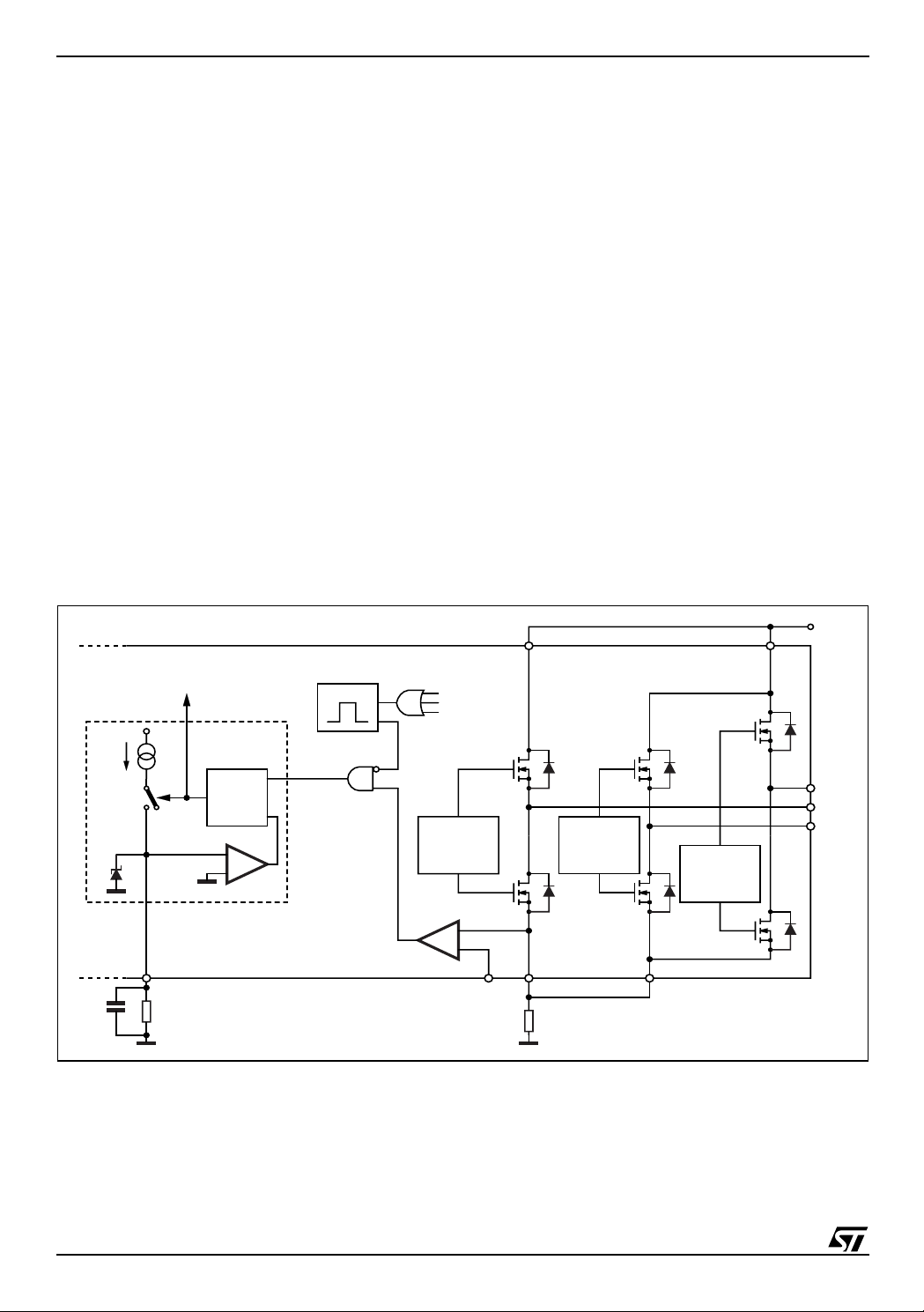
condition. The L6235 is a highly i ntegrated, mixed-si gnal power IC that allows to easily design a co mplete motor
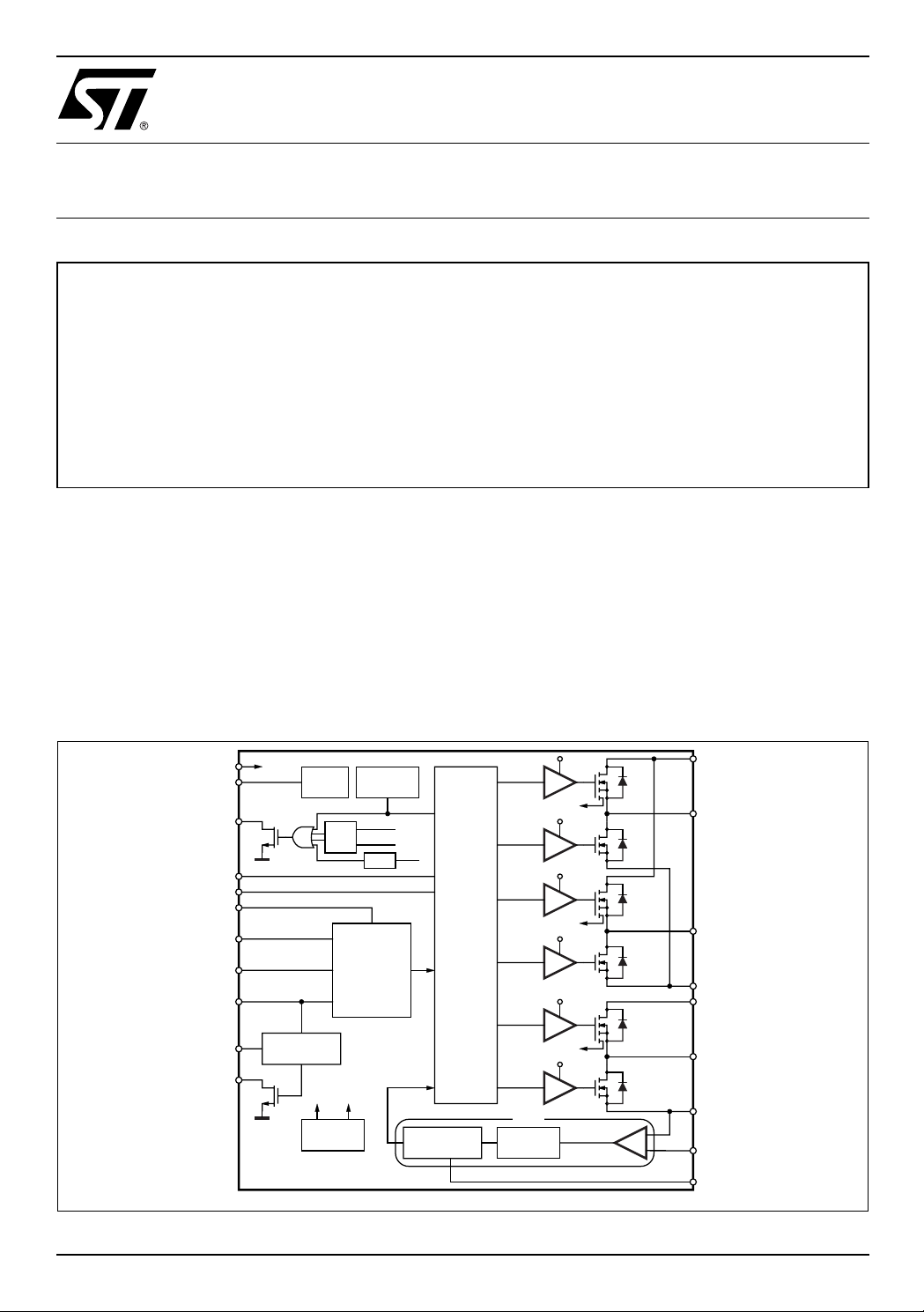
control system for BLDC motor. Figure 1 shows the L6235 block diagram. The IC integrates six Power DMOS,
a centralized logi c circuit to decode hall effect sensors and a constant t
chronous mode) plus other added features for safe operation and flexibility.
PWM current contro l technique (Syn-
OFF
Figure 1. L6235 Block Diagram.
VBOOT V
VCP
DIAG
BRAKE
FWD/REV
RCPULSE
TACHO
BOOT
EN
H
3
H
2
H
1
TACHO
MONOSTABLE
CHARGE
PUMP
OCD
HALL-EFFECT
10V 5V
VOLTAGE
REGULATOR
THERMAL
PROTECTION
OCD1
OCD2
OCD
SENSORS
DECODING
LOGIC
OCD3
ONE SHOT
MONOSTABLE
GATE
LOGIC
PWM
MASKING
TIME
V
BOOT
OCD1
10V
V
BOOT
OCD2
10V
V
BOOT
OCD3
10V
COMPARATOR
SENSE
VS
A
OUT
1
OUT
2
SENSE
A
VS
B
OUT
3
SENSE
B
+
-
VREF
RCOFF
D99IN1095B
October 2003
1/39
Page 2

AN1625 APPLICATION NOTE
Table of Contents
1 INTRODUCTION................................................................................................................................ 1
2 DESIGNING AN APPLICATION WI TH L623 5 ...................................................................................3
2.1 Current Ratings........................................................................................................................3
2.2 Voltage Rating s and Operating Range ....................................................................................3
2.3 Choosing th e Bulk Capacitor....................................................................................................5
2.4 Layout Considerations.............................................................................................................5
2.5 Sensing Resisto r.......... ............... ........................................................ ............................. ....... .7
2.6 Charge pump external components.........................................................................................8
2.7 Sharing the Charge Pump Circuitry .........................................................................................9
2.8 Reference Voltage for PWM Current Control.........................................................................10
2.9 Input Logic pins......................................................................................................................11
2.10 DIAG pin.................................................................................................................................11
2.11 Programmable off-time Monostable.......................................................................................12
2.11.1 Off-time Selection and minimum on-time ........................................................................14
2.11.2 Slow Decay Mode ...........................................................................................................14
2.12 Over Current Detection.........................................................................................................16
2.13 Powe r Management...............................................................................................................20
2.13.1 Maximum output current vs. selectable devices..............................................................20
2.13.2 Power Dissipation Formulae...........................................................................................21
2.14 The decoding logic................................................................................................................24
2.15 Tacho Outp ut and Speed Loop.............................................................................................25
2.15.1 Static performance - Speed Regulation vs. Resistant Torque: .......................................28
2.15.2 Dynamic performance:....................................................................................................29
2.15.3 Loop Stability:........................................................................................... .......................30
2.15.4 Reference voltage ripple: ................................................................................................30
2.16 Brake.....................................................................................................................................31
3 APPLICATION EXAM PL E.............................. ......................................................... .........................32
4 APPENDIX - EVALUATI ON BO ARD S...................................................................... .......................34
4.1 PractiSPIN............................................................................. .................................................34
4.2 EVAL6235N ...........................................................................................................................35
4.2.1 Important Not e s......... ................................... ......................................................... ....... ....36
5 REFERENCES....................................................................................... ..........................................39
2/39
Page 3
AN1625 APPLICATION NOTE
2 DESIGNING AN APPLICATION WITH L6235
2.1 Current Ratings
With MOSFET (DMOS) devices, unlike bipolar transistors, current under short circuit conditions is, at first approximation, limited b y the R
and the two V
and VSB pins are rated for a maximum of 2.8 A r.m.s. and 5.6 A peak (typical values). These
SA
values are meant to avoid damaging metal structures, including the metallization on the die and bond wires. In
practical applications, though, maximum allowable current is less than these values, due to power dissipation
limits (see Power Management section).
The device has a built-in Over Current Detection ( OCD) that allows protection against shor t circuits between the
outputs and between an output and ground (see Over Current Detection Section).
2.2 Voltage Ratings and Operating Range
The L6235 requires a single supply voltage (VS), for the motor supply. Internal voltage regulators provide the
5V and 10 V required for the internal circuitry. The operating range for V
undesirable low supply voltage an Under Voltage Lock Out (UVLO) circuit shuts down the device when supply
voltage falls below 6 V; to resume normal operating conditions, V
vided to avoid false intervention of the UVLO function during fast V
DMOS's R
is a function of the VS supply voltage. Actually, when VS is less than 10V, R
DS(ON)
affected, and this is particularly true for the High Side DMOS that are driven from V
obtained through a charge pump fr om the internal 10V supply, which will tend to r educe i ts output v oltage when
goes below 10V. Figure 2 shows the supply voltage of the high side gate drivers (V
V
S
supply voltage (V
).
S
of the DMOS themselves and c ould reach v er y high values. L6235 Out pi ns
DS(ON)
is 8 to 52 V. To prevent working into
S
must then exceed 7 V. The hy steresis is pro-
S
ringings. It should be noted, however, that
S
DS(ON)
supply. This supply is
BOOT
- VS) versus the
BOOT
is adversely
Figure 2. High side gate drivers supply voltage versus supply volta ge.
8
7.6
V
BOOT
- V
[V]
7.2
S
6.8
6.4
6
8 8.5 9 9.5 10 10.5
VS [V]
Note that VS must be connected to both VSA and VSB because the bootstrap vol tage (at V
pin) is the same
BOOT
for the two H-bridges. The integrated DMOS have a rated Drain-Source breakdown voltage of 60 V. However
V
should be kept b elow 52 V , si nce i n nor mal workin g condi tions th e DMOS see a Vds vo ltage that wil l ex ceed
S
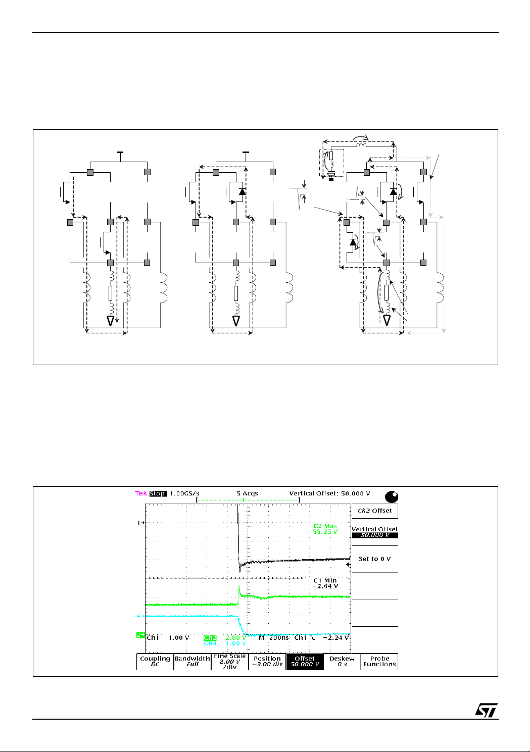
supply. In particular when a high-side DMOS turns off due to a phase change (OUT1 in Figure 3), if one of
V
S
the other outputs (OUT2 in Figure 3) is high (during the off-time all active bridges turn their high-side on) the
load current starts flowing in the low-side freewheeling diode and the SENSE pin sees a negative spike due to
a not negligible parasitic inductance of the PCB path from the pin to GND. This spike is followed by a stable
negative voltage due to the drop on R
. The output pin sees a similar behavior, but with a slightly larger
SENSE
voltage due to the forward recovery time of the integrated freewheeling diode and the forward voltage drop
across it. Typical duration of this spike is 30 ns. At the same time, the OUT2 pin (in the example of Figure 3)
3/39
Page 4
AN1625 APPLICATION NOTE
sees a voltage above VS, due to voltage drop across the high-side (integrated) freewheeling diode, as the current reverses direction and flows into the bulk capacitor. It turns out that the highest differential voltage is observed between two OUT pins when a phase change turns a high-side off during an off-time, and this must
always be kept below 60 V [2].
Figure 3. Currents and voltages if a phase change turns a high-side off during off-time.
Current starts
V
*I
S
PCB Parasit ic
Inductance
flowing in the
third half bridge
Bulk
Capacitor
Equivalent
Circuit
R
SENSE
*I+V
ESR
ESL
F(Diode)
PCB Parasitic
Inductance
R
SENSE
on-time off-time during of f-time
a phase change can occur
Figure 4 shows the voltage waveforms at the OUT pins referring to a possible practical situation, with a peak
output current of 2.8 A , V
= 52 V, R
S
= 0.33 Ω, TJ = 25 °C (approxim ately) and a good P CB layout. Below
SENSE
ground spike amplitude is -2.64 V for one output; the other OUT pin is at about 55 V. In these conditions, total
differential voltage reaches almost 60 V, which is the absolute maximum rating for the DMOS. Keeping differential voltage between two Output pins within rated values is a must that can be accomplished with proper selection of Bulk capacitor value and equivalent series resistance (ESR), accordi ng to current peaks and adopting
good layout practices to minimize PCB parasitic inductances (see below) [2].
Figure 4. Voltage at the two outputs if a phase change turns a high-side off during off-time.
OUT1
OUT2
SENSE
4/39
Page 5

AN1625 APPLICATION NOTE
2.3 Choosing the Bulk Capacitor
Since the bulk capacitor, placed between VS and GND pins, is charged and discharged during IC operation, its
AC current capability must be greater than the r.m.s. value of the charge/discharge current. This current flows
from the capacitor to the IC during the on-time (t
power supply during off-time) to the capacitor during the off-time (t
into the bulk capacitor depends on peak output current, output current ripple, switching frequency, duty-cycle.
It also depends on power supply characteristics. A power supply with poor high frequency performances (or
long, inductive connecti ons to the IC) will cause the bulk c apacitor to be recharged sl owly: the higher the current
control switching frequency, the higher the current ripple in the capacitor; r.m.s. current in the capacitor, however, does not exceed the r.m.s. output current. Bulk capac itor value ( C) and the ESR determine the amount of
voltage ripple on the c apacitor itself and on the IC. Neglecting the output current rippl e and assuming tha t during
the on-time the capacitor is not recharged by the power supply, the voltage at the end of the on-time is
VSI
) and from the IC (during some phase changes; from the
ON
). The r.m.s. value of the current flowing
OFF
t
ESR
⋅–
OUT
-------- -+
ON
C
where I
is the output current. Usually (if C>100 µF) the capacitance role is much less than the ESR, then
OUT
supply voltage ripple can be estimated as
ESR⋅
I
OUT
For Example, if a max imum ri pple of 500 mV i s all owed and I
0.5V
------------
ESR
2A
Note that additional ripple is due to parasitic inductances on V
= 2 A, the capac itor E SR s hould be lower than
OUT
250mΩ=<
PCB tracks (see Voltage Ratings and Operating
S
Range section).
Actually, current sunk by V
and VSB pins of the device is subject to higher peaks due to reverse recovery
SA
charge of internal freewheeling diodes. Duration of these peaks is, tough, very short (100÷200 ns) and can be
filtered using a small value (100÷20 0 nF), good quality ceramic capaci tor, connected as close as possible to the
V
, VSB and GND pins of the IC. Bulk capacitor will be chosen with maximum operating voltage 25% greater
SA
than the maximum supply voltage, considering als o power supply toler ances . For exa mple, w ith a 48 V nomi nal
power supply, with 5% tolerance, maximum voltage is 50.4 V, then operating voltage for the capacitor should
be at least 63 V.
2.4 Layout Considerations
Working with devices that combine high power switches and control logic in the same IC careful attention has
to be paid to the PCB lay out. In extreme cases, Power DMOS commutation can i nduce nois es that could c ause
improper operation in the logic section of the device. Noise can be radiated by high dv/dt nodes or high di/dt
paths, or conducted through G ND or Supply connectio ns. Logic connec tions, es pecial ly hi gh-i mpedance nodes
(actually all logic inputs, see further), must be kept far from switching nodes and paths. With the L6235, in particular, external components for the charge pump circuitry should be connected together through short paths,
since these components are subject to voltage and current switching at relatively high frequency (600 kHz). Primary mean in minimizing conducted noise is working on a good GND layout (see Figure 5).
5/39
Page 6
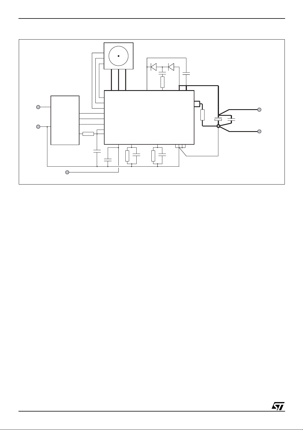
AN1625 APPLICATION NOTE
3
-
Figure 5. Typ ic a l App li ca ti on and Layout suggest io ns.
Phase
Brushless
DC Motor
D1
C5
R4
D2
C8
V
CP
SA VSB
SENSE
A
SENSE
B
R5
C6
C7
+
VS = 8 ÷ 52 V
-
GND GND
GND GND
C4
+
Logic Supply
3.3 ÷ 5 V
-
µC
or
Custom Logic
V
= 0 ÷1V
ref
3
V
BOOT
L6235
C3
R3
RC
PUL SE
OUT
OUT1 OUT
2
H1
H2
H3
FWD/REV
BRAKE
TACHO
DIAG
R1
EN
V
ref RCOFF
C1
C2
R2
High cur rent GND tracks (i .e. the trac ks con nected to the sens ing r esistor) m ust be c onnecte d dire ctly to the ne gative terminal of the bulk capacitor. A good quality, high-frequency bypass capacitor is also required (typically a
100 nF÷200 nF ceramic would suffice), since electrolytic capacitors show a poor high frequency performance.
Both bulk electrolytic and high frequency bypass capacitors have to be connected with short tracks to V
SA
, V
SB
and GND . On the L62 35 GND pins are th e Logic GND, sinc e only the q uiescent curren t flow s throu gh them . Logic
GND and Power GND should be connected together in a single point, the bulk capacitor, to keep noise in the
Power GND from affecting Logic GND. Specific care should be paid layouting the path from the SENSE pins
through the sen sing r esistor to the negative termin al of the bulk ca pacitor (P ower Ground) . These tracks mus t be
as short as possible in order to minimize parasitic inductances that can cause dangerous voltage spikes on
SENSE and OUT pins (see the Voltage Ratings and Operating Range section); for the same reason the capacitors on V
section for inf ormat ion on selec ting the sens e resis tors. Tr aces th at connect to V
, VSB and GND pi ns sho uld be ver y close to the GN D and sup ply pin s. Refe r to the Sens ing R esisto rs
SA
, VSB, SENSEA, SENSEB, and
SA
the three OUT pins must be d esi gne d w ith a dequ ate w id th, s inc e hig h cu rr ents ar e fl owing through the se tra ces ,
and layer ch anges sh ould be avoide d. Should a lay er ch ange prove necess ary, m ultiple an d large via holes have
to be used. A wide GND copper area can be used to improve power dissipation for the device.
Figure 6 shows two typical situations that must be avoided. An important consideration about the location of the
bulk capacitor is the ability to absorb the inductive energy from the load, without allowing the supply voltage to
exceed the maximum rating. The diode shown in Figure 6 prevents the recirculation current from reaching the
capacitors and will res ult in a high voltage on the IC pins th at can destroy the device. H aving a switch or a power
connection that can dis connect the c apacitors from the IC, w hile there is stil l c ur rent in the motor, will a lso result
in a high voltage transient since there is no capacitance to absorb the recirculation current.
6/39
Page 7
AN1625 APPLICATION NOTE
Figure 6. Two situations that must be avoided.
DON’T put a diode here!
Recircul ating c urrent c annot flow into the
bulk capac itor and caus es a high voltage
spike that can dest roy the IC.
+
C7
VS = 8 ÷ 52 V
L6235
GND
V
SA VSB
SENSE
A
SENSE
B
R5
C6
GND
GND
GND
-
DON’T conne ct the Logic GND here
Voltage dro p due t o c urrent in s ens e
path can disturb logic GND.
2.5 Sensing Resistor
Motor winding current flows through the sensing resistor, causing a voltage drop that is used, by the logic, to
control the peak value of the load current. Two issues must be taken into account when choosing the R
value:
■ The sensing resistor dissipates energy and provides dangerous negative voltages on the SENSE pins
during the current recirculation. For this reason the resistance of this component should be kept low.
■ The voltage drop across R
parator. The lower is the R
SENSE
SENSE
to the input offset of the current sense comparator: too small values of R
A good compromise is calculating the sensi ng resistor value so that the voltage drop , corresponding to the peak
current in the load (Ipeak), is about 0.5 V: R
It should be clear that sensing resistor must absolutely be non-inductive type in order to avoid dangerous negative spikes on SENSE pins. Wire wounded resistors cannot be used here, while Metallic film resistors are recommended for their high peak current capability and low inductance. For the same reason the connections
between the SENSE pins, C6, C7, V
(see also the Layout Considerations section).
SENSE
is compared to the reference voltage (on Vref pin) by the internal com-
value, the higher is the peak current error due to noise on Vref pin and
must be avoided.
SENSE
= 0.5 V / Ipeak.
SENSE
, VSB and GND pins (see Figure 5) must be taken as short as possible
SA
The average power dissipated by the sensing resistor is:
PRI
D is the duty-cycle of the PWM current control, I
2
R
rms
SENSE
is the r.m.s. value of the load current.
rms
;
D⋅⋅≈
Nevertheless, sensing resistor power rating should be chosen taking into account the peak value of the dissipated power:
where I
is the peak value of the load current.
pk
P
2
I
R
pk
R
⋅≈
SENSE
,
Using multiple resistors in parallel will help obtaining the required power rating with standard resistors, and re-
7/39
Page 8
AN1625 APPLICATION NOTE
duce the inductance.
R
The following table shows R
tolerance reflects on the peak current error: 1% resistors should be preferred.
SENSE
recommended values (to have 0.5V drop on it) and power ratings for typical
SENSE
examples of current peak values.
I
pk
0.5 1 0.25
1 0.5 0.5 2 X 1Ω, 0.25W paralleled
1.5 0.33 0.75 3 X 1Ω, 0.25W paralleled
2 0.25 1 4 X 1Ω, 0.25W paralleled
R
SENSE
Value
[Ω]
R
SENSE
Power Rating
[W]
Alternatives
2.6 Charge pump external components
An internal oscillator, with its output at CP pin, switches from GND to 10 V with a typical frequency of 600 kHz
(see Figure 7).
Figure 7. Charge Pump .
VS + 10 V - VD1 - V
V
BO OT
D2
D1
C5
R4
CP
VS + 10 V - V
D2
V
SA VSB
D1
V
S
- V
D1
f = 600 kHz
C8
10 V
R
R
DS(O N)
DS(ON)
= 70Ω
= 70Ω
Charge Pum p
Oscillator
10 V
5 V
10 V
f = kHz
600
To High-Side
Gate Drivers
L6235
When the oscillator output is at ground, C5 is charged by VS through D2. When it rises to 10 V, D2 is reverse
biased and the charge flows from C5 to C8 through D1, so the V
imum voltage of V
With a differential voltage between V
current drawn by the V
+ 10 V - VD1 - VD2, which supplies the high-side gate drivers.
S
pin is 1.85mA.
BOOT
and V
S
of about 9V and the bridges switching at 50 kHz, the typical
BOOT
Resistor R4 is added to r educe the maximum current in the exter nal components and to reduce the slew rate of
the rising and falling edges of the voltage at the CP pin, in order to minimize interferences with the rest of the
circuit. For the same reason car e must be taken in realiz ing the PC B layout of R 4, C5, D1, D2 connections ( see
also the Layout Considerations section). Recommended values for the charge pump circuitry are:
8/39
pin, after a few cycles, reaches the max-
BOOT
Page 9
D1, D2 : 1N4148
AN1625 APPLICATION NOTE
R4 : 100
Ω (1/8 W)
C5 : 10 nF 100V ceramic
C8 : 220 nF 35V ceramic
Due to the high charge pump frequency, fast diodes are required. Connecting the cold side of the bulk capacitor
(C8) to V
= 100
instea d of GND the ave rage cu rre nt in the ex ter nal di odes during operati on is le ss tha n 10 mA (with R4
S
Ω
); at star t up (w h en VS is provided t o the IC) is less than 200 mA while the reverse voltage is about 10 V
in all co nd iti on s. 1N 41 48 dio de s withstand about 200 mA DC (1 A pea k ), and the max i mu m reverse vo lta ge is 75
V, so they should fit for the majority of applications.
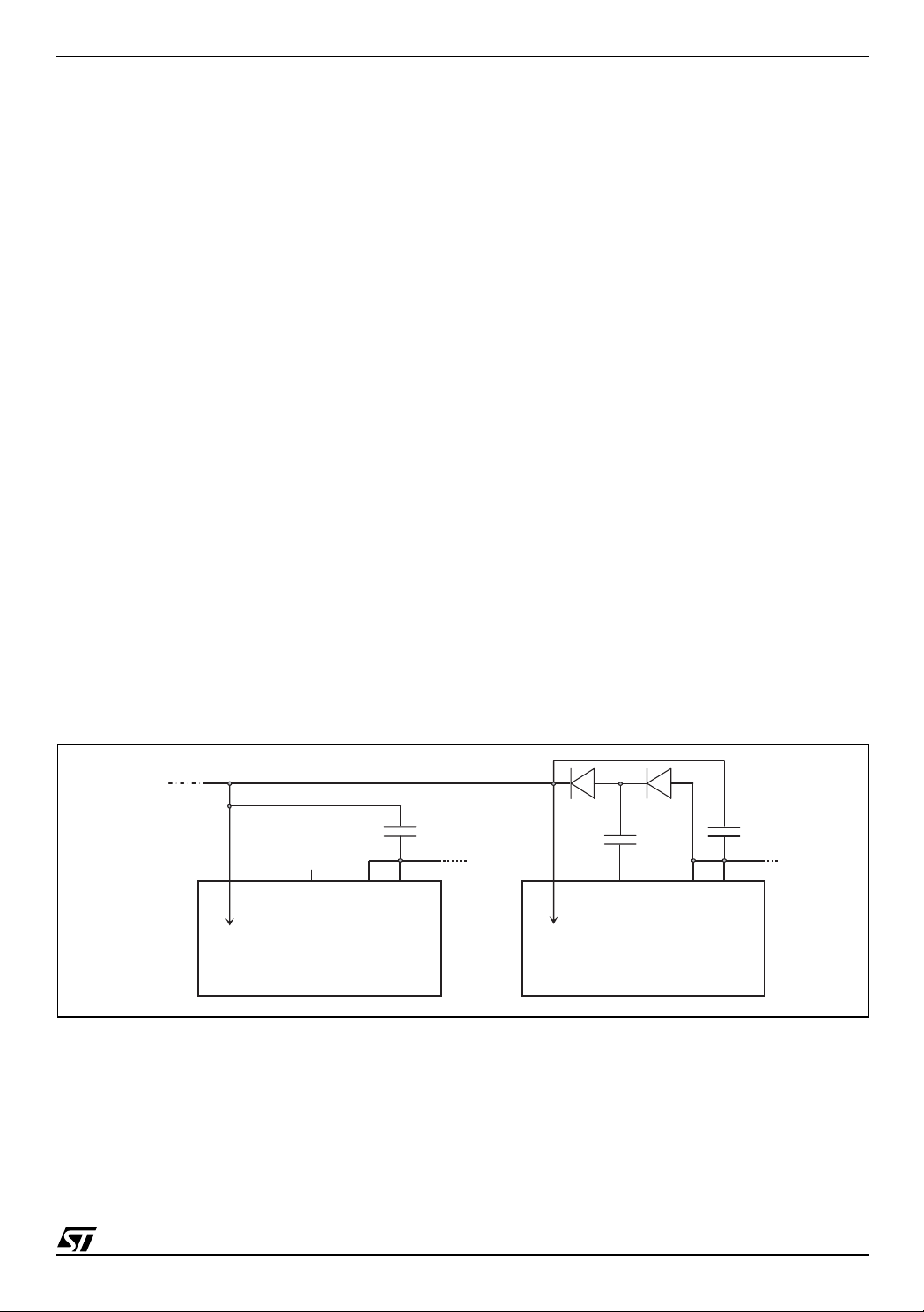
2.7 Sharing the Charge Pump Circuitry
If more than one device is used in the applic ation, it's possible to use the char ge pump from one L6235 to suppl y
the V
Figure 8. A 100 nF capacitor (C8) should be connected to the V
Supply voltage pins (V
pins of several ICs. The unused CP pins on the slaved devices are left unconnected, as shown in
BOOT
) of the devices sharing the charge pump must be connected together.
S
pin of each device.
BOOT
The higher the number of devices sharing the same charge pump, the lower will be the differential volt age available for gate drive (V
- VS), causing a higher R
BOOT
for the high side DMOS, so higher dissipating po wer.
DS(ON)
In this case it's recommended to omit the resistor on the CP pin, obtaining a higher current capability of the
charge pump circuitry.
Better performance can also be obtained using a 33 nF capacitor for C5 and using schottky diodes (for example
BAT47).
Sharing the same charge pump ci rcuitr y fo r mor e than 3÷4 devi ces is not recommended, sinc e it wil l reduce the
V
voltage increasing the high-side MOS on-resistance and thus power dissipation.
BOOT
Figure 8. Sharing the charge pum p circuitry.
To other Devices
V
BO OT
To High-Side
Gate Drivers
V
V
SA
CP
SB
L6235
C18 = 100 nF
D2 = BAT47
CP
V
SA VSB
C8 = 100nF
V
BOOT
To High-Side
Gate Drivers
D1 = BAT47
C5 = 33nF
L6235
9/39
Page 10
AN1625 APPLICATION NOTE
2.8 Reference Voltage for PWM Current Control
The device has an analog input, Vref, connected to the internal sense comparator, to control the peak value of
the motor current through the integrated PWM circuitry. A fixed reference voltage can be easily obtained through
a resistive divider from an available 5 V voltage rail (maybe the one supplying the µC or the rest of the application) and GND.
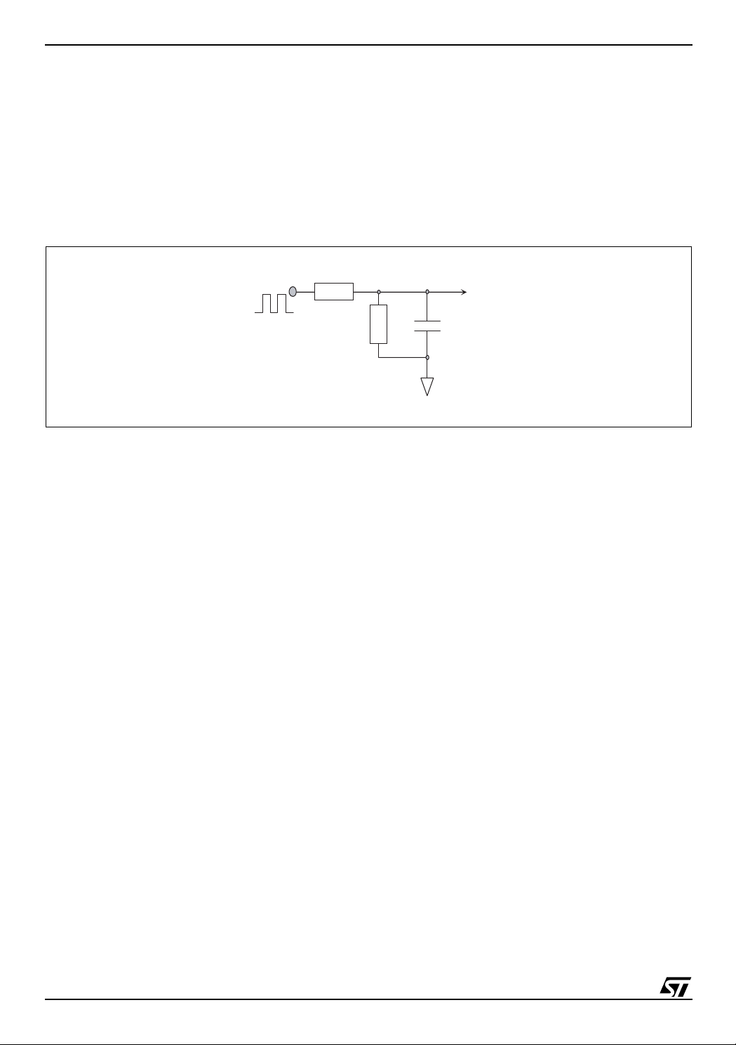
A very simple way to obtain a variable voltage without using a DAC is to low-pass filter a PWM output of a µC
(see Figure 9).
Figure 9. Obt ain in g a va ri abl e v ol ta ge t hro ugh a PWM ou t put of a µC .
PWM Output
of a µC
R
LP
R
DIV
GND
V
ref
C
LP
Assuming that the PWM output swings from 0 to 5V, the resulting average voltage will be
5V DµCR
⋅⋅
-----------------------------------------=
RLPR
where D
V
ref
is the duty-cycle of the PWM output of the µC.
µC
Assuming that the µC output impedance is lower than 1k
DIV
+
DIV
Ω,
with RLP = 56kΩ, R
= 15kΩ, CLP = 10nF and a
DIV
µC PWM switching fr om 0 to 5V at 100kHz , the l ow pass fi lter tim e consta nt is about 0.12 ms an d the remai ning
ripple on the V
voltage will be about 20 mV. Using higher values for RLP, R
ref
and CLP will reduce the ripple,
DIV
but the reference voltage will tak e more time to vary after changing the duty -cycle of the µC PWM, an d too high
values of R
As sensing resistor value is typically kept small, a small noise on V
will also incr ease the impedance of the V
LP
net at low frequencies, causi ng a poor noise immuni ty.
ref
input pins might cause a considerable error
ref
in the output current. It's then recommended to decouple this pin with a ceramic capacitor of some tens of nF,
placed very close to Vref and GND pins. Note that Vref pin cannot be left unconnected, while, if connected to
GND, zero current is not guaranteed due to voltage offset in the sense comparator. The best way to cut down
(IC) power consumpti on and clear the l oad current is pul ling down the EN pin. With very small refer ence voltage,
PWM integrated circuitry can loose control of the current due to the minimum allowed duration of t
(see the
ON
Programmable off-time Monostable section).
10/39
Page 11
AN1625 APPLICATION NOTE
2.9 Input Logi c pin s
H1, H2, H3, FWD/REV, BRAKE, ENABLE, are CMOS/TTL compatible logic input pins. The input comparator
has been realized with hysteresis to ensur e the required noise immunity . Typical val ues for turn-on and turn-off
thresholds are V
electro-static discharge), and can be directly connected to the logic outputs of a µC; a series resistor is generally not
recommended, as it could hel p induct ed noise to dist urb the input s. All logic pi ns enfor ce a specifi c behavior and cannot be left unconnected. If connected to the DIAG pin, EN pin must be driven through a series resi stor of 2.2 k
imum (for 5 V logic), to allow the voltage at the pin to be pulled below the turn-off threshold (see below).
Figure 10. Logic input pins.
= 1.8 V and V
TH(ON)
TH(OFF)
= 1.3 V.
H1, H2 H3
FWD/REV, BRAKE
ENABLE
Pins are ESD protected (see Figure 10) (2kV human-body
5 V
,
ESD
Protection
,
Ω
min-
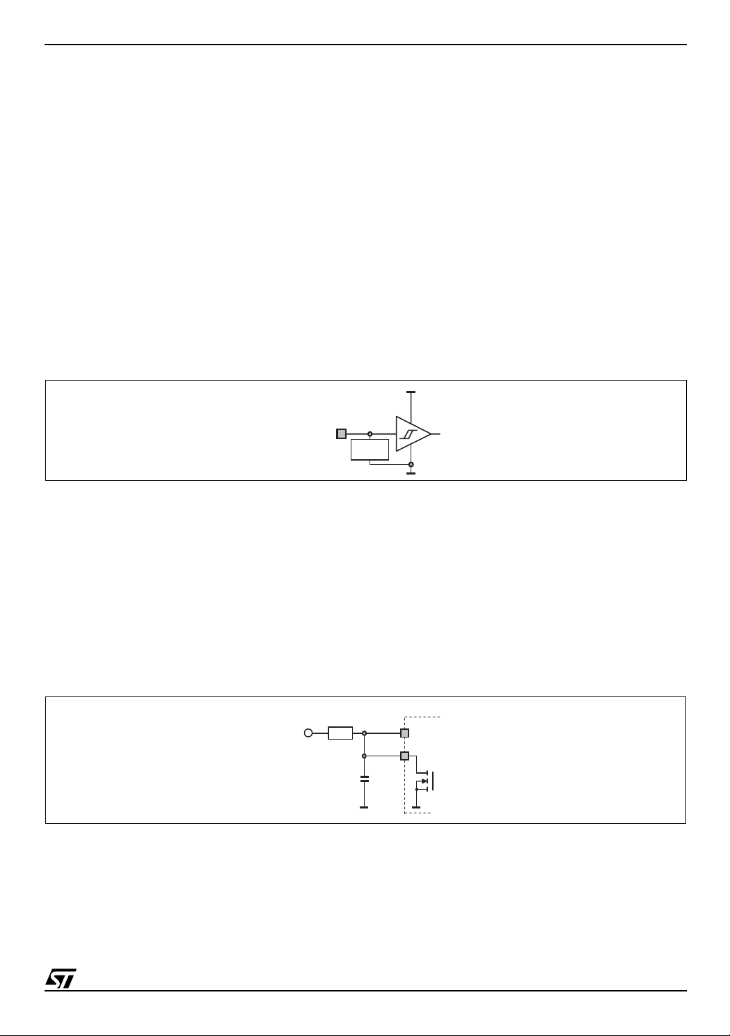
2.10DIAG pin
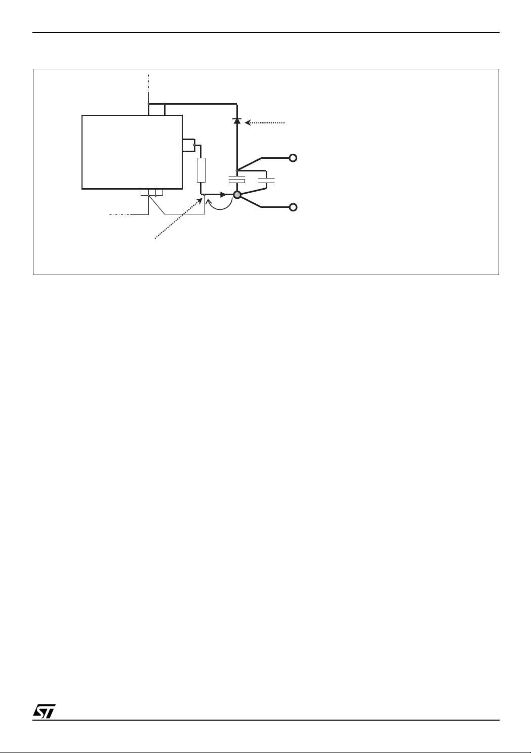
DIAG pin is an open-drain output pul led to GND in case of ov ercurrent or over temperatur e conditions. Connecting this pin to EN will allow the internal open drain to disable all the power DMOS of the L6235, provided that
the EN pin is driven through a resistor (see Input Logic pins).
A capacitor (C1 in Figure 5 and Figure 11) conne cted between EN and DIAG pins and GND is als o recommended, to reduce the r.m.s. value of the output current when overcurrent conditions persist (see Over Current Protection section).
Figure 11. DIAG pin.
µC or Logic
Output
R1
C1
EN
DIAG
11/39
Page 12
AN1625 APPLICATION NOTE
2.11Programma ble off-time Monostable
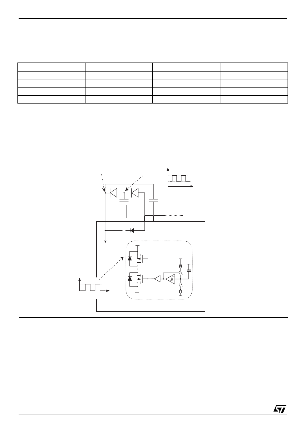
The L6235 includes a constant off time PWM Current Controller. The current control circuit senses the bridge
current by sensing the voltage drop across an external sense resistor connected between the source of the
three lower power MOS transistors and ground, as shown in Figure 12. As the current in the motor increases
the voltage across the sense r esistor incr eases pr oportionall y. When the voltage drop across the s ense r es istor
becomes greater than the voltage at the reference input pin VREF the sense comparator triggers the
monostable switching the bridge off. The power MO S re main off for the time set by the monos table and the motor current recirculates ar ound the upper half of the bridge in S low Decay Mode as described in the next sec tion.
When the monostable times out, the bridge will again turn on. Since the internal dead time, used to prevent
cross conduction in the bridge, delays the turn on of the power MOS, the effective Off Time t
the monostable time plus the dead time.
Figure 13 shows the typical operating waveforms of the output current, the voltage drop across the sensing resistor, the pin RC vol tage and the status of the bridge. More d etails regarding the S ynchronous Rectificati on and
the output stage configuration are included in the next section.
Immediately after the Power MOS turn on, a high peak current flows through the sense resistor due to the reverse recovery of the freewheeling diodes. The L6235 provides a 1µs Blanking Time t
BLANK
comparator output so that the current spike cannot prematurely retrigger the monostable.
is the sum of
OFF
that inhibits the
Figure 12. PWM Current Controller Simplified Schematic
VS
B
TO GATE
LOGIC
5mA
S
(0) (1)
5V
RCOFF
C
OFF
R
OFF
Q
R
-
+
2.5V
BLANKING TIME
MONOST ABLE
1µs
MONOST ABLE
SET
COMP ARATOR
BLANKER
SENSE
FROM THE
LOW-SIDE
GATE DRIVERS
DRIVERS
+
DEAD TIME
+
-
VREF
R
SENSE
SENSE
DRIVERS
+
DEAD TIME
B
SENSE
DRIVERS
+
DEAD TIME
A
D02IN1380
VS
A
VS
OUT
OUT
OUT
2
3
1
12/39
Page 13

Figure 13. Output Current Regulation Waveforms
I
OUT
V
REF
R
SENSE
AN1625 APPLICATION NOTE
V
SENSE
V
REF
0
V
RC
5V
2.5V
ON
OFF
SYNCHRONOUS RECTIFICATION
D02IN1351
t
OFF
1µs t
BLANK
t
ON
Slow Decay Slow Decay
t
RCRISE
t
RCFALL
1µs t
DT
BC
DDA
t
RCFALL
BC
t
OFF
1µs t
t
RCRISE
1µs t
BLANK
DT
Figure 14 shows the magnitude of the Off Time t
calculated from the equations:
t
t
where R
20K
0.47nF ≤ C
t
= 0.6 · R
RCFALL
= t
OFF
RCFALL
and C
OFF
Ω ≤
= 1µs (typical value)
DT
R
OFF
OFF
OFF
· C
OFF
OFF
· C
OFF
+ t
OFF
+ tDT = 0.6 · R
are the external component values and tDT is the internally generated Dead Time with:
≤ 100K
Ω
≤ 100nF
Therefore:
t
OFF(MIN)
t
OFF(MAX)
These values allow a sufficient range of t
The capacitor value chosen for C
Rise Ti me t
= 6.6µs
= 6ms
to implement the drive circuit for most motors.
OFF
also affects the Rise Time t
will only be an issue if the capacitor is not completely charged before the next time the
RCRISE
OFF
monostable is triggered. Therefore, the On Time t
be bigger than t
can not be smaller than the minimum on time t
for allowing a good current regulation by the P WM stage. Further more, the On Time t
RCRISE
ON(MIN)
versu s C
OFF
DT
, which depends by motors and supply parameters, has to
ON
OFF
RCRISE
and R
values. It can be approximately
OFF
of the voltage at the pin RC
OFF
.
. The
ON
13/39
Page 14

AN1625 APPLICATION NOTE
t
> 1.5µs (typ. value)=
ONtON MIN()
t
ONtRCRISEtDT
t
RCRISE
= 600 · C
2.11.1 Off-time Selection and minimum on-time
Figure 14 also shows the lower limit for the On Time tON for having a good PWM current regulation capacity. It
has to be said that t
smaller than t
RCRISE
stant.
So, small C
value gives more flexibility for the applications (allows smaller On Time and, therefore, higher
OFF
switching frequency), but, the smaller is the value for C
performance.
Figure 14. Off-time selection and minimum on-time.
–>
OFF
is always bigger than t
ON
ON(MIN)
because the device imposes this condition, but it can be
- tDT. In this last case the device continues to work but the Off Time t
, the more influential will be the noises on the circuit
OFF
4
1.10
1.10
3
R = 100 kΩ
R = 47 kΩ
R = 20 kΩ
is not more con-
OFF
100
to f f [u s]
100
to n ( m in ) [ u s]
2.11.2 Slow Decay Mode
10
1
0.1 1 10 100
10
1
0.1 1 10 100
Coff [nF]
Coff [nF]
Figure 15 shows the operation of the bridge in the Slow Decay mode during the Off Time. At any time only two
legs of the three-phas e br idge are acti ve, therefor e only the two acti ve l egs of the br idge are s hown in the figure
and the third leg will be off. At the start of the Off Time, the lower power MOS is switched off and the current
14/39
Page 15

AN1625 APPLICATION NOTE
µ
/
recirculates around the upper half of the bridge. Sinc e the voltage across the coil is low, th e current decays slowly. After the Dead Time the upper power MOS is operated in the synchronous rectification mode reducing the
impedance of the freewheeling diode and the related conducting loss es. When the monostable times out, upper
MOS that was operating the synchronous mode turns off and the lower power MOS is turned on again after
some delay set by the Dead Time to prevent cross conduction.
Figure 15. Slow Decay Mode Output Stage Configurations
A) ON TIME B) 1µs DEAD TIME C) SYNCHRONOUS
D01IN1336
RECTIFICATION
D) 1µs DEAD TIME
In some conditions (short off-time, very low regulated current, high motor winding L / R) the system may need
an on-time shorter than 1.5 µs. In these cases the PWM current controller can loose the regulation.
Figure 16 shows the operation of the circuit in this condition. When the current first reaches the threshold, both
the high-side are turned on for a fixed time and the current decays.
During the following on-time cur rent increas es above the threshold, but the br idg e cannot be turned off unti l the
minimum on-time expires. Since current increases more in each on-time than it decays during the off-time, it
keeps growing during each cycle, with steady state asymptotic value set by duty- c ycle and load DC resis tance:
the resulting peak current will be I
= VS × D / R
pk
, where D = tON / (tON+t
LOAD
) is the duty-cycle and R
OFF
LOAD
is the load resistance.
Figure 16. Minimum on-time can cause the PWM controller to loose the regulation.
minimum tON
is about 1.5
V
R
ref
SENSE
s
needed tON is
less
than 1.5 µs
15/39
Page 16

AN1625 APPLICATION NOTE
2.12 Over Curre nt Detection
To implement an O ver Cur rent (i.e. shor t ci rcuit) Pr otection, a dedi cated Over Cur rent D etection (OCD) circ uitry
(see Figure 17 for a simplified schem atic) senses the current in each high side. P ower DMOS are actually made
up with thousands of individual identical cells, each carrying a fraction of the total current flowing. The current
sensing element, connected in parallel to the Power DMOS, is made only with few such cells, having a 1:N ratio
compared to the power DMOS. The total drain current is split between the output and the sense element according to the cell ratio. Sensed current is, then, a small fraction of the output current and will not contribute
significantly to power dissipation.
Figure 17. Over Current Detection simplified circuitry.
OUT
OUT
VS
1
2
A
OUT3VS
B
µC or LOGIC
V
DD
HIGH SIDE DMOS
I
1
POWER SENSE
DS(ON)
1 cell
INTERNAL
OPEN-DRAIN
TO GATE
LOGIC
R
EN
EN
C
EN
DIAG
R
40Ω TYP.
POWER DMOS
OCD
COMPARATOR
n cells
I1 / n
I1+I2 / n
I
REF
OVER TEMPERATURE
I
REF
HIGH SIDE DMOS HIGH SIDE DMOS
+
I
2
POWER DMOS
n cells
I2/ n
POWER SENSE
1 cell
I3/ n
D02IN1381
I
POWER DMOS
3
n cells
POWER SENSE
1 cell
This sensed current is compared to an internally generated reference to detect an over current condition. An
internal open drain mosfet turns on when the sum of the currents in the bridges 1 and 2 or the current in the
bridge 3 reaches the threshold (5.6A typical value); the open drain is available at the DIAG pin for diagnostic
purposes or to ensure an over current protection, connecting EN and DIAG together and using an RC network
(see Figure 17).
16/39
Page 17

AN1625 APPLICATION NOTE
E
Figure 18. Over Current Operation after a short circuit between an OUT pin and GND. EN and DIAG
pins are connected together.
t
t
OCD(ON)
I
S OVER
DELAY
Output Current
t
EN(FALL)
t
D(OFF)EN
t
DISABLE
Output Current
t
D(ON)EN
V
TH(OFF)
t
OCD(OFF)
t
DISABLE
EN
= DIAG
V
TH(ON)
V
EN(LOW)
t
EN(RISE)
= DIAG
N
Figure 18 shows the device operating in overcurrent condition (short to ground). When an over current is detected the internal open drain mo sfet pull s the E N pin to GND s witching off al l 6 pow er DMOS of the devic e and
allowing the cur rent to decay . Under a persistent over current c ondition, lik e a short to ground or a shor t between
two output pins, the external RC network on the EN pin (see Figure 17) reduces the r.m.s. value of the output
current by imposing a fixed disable-time after each over current occurrence. The values of R
and CEN are
EN
selected to ensure proper operation of the device under a short circuit condition. When the current flowing
through the high side DMOS reaches the OCD threshold (5.6 A typ.), after an internal propagation delay
(t
OCD(ON)
(V
) the open drain starts discharging CEN. When the EN pin voltage falls below the turn-off threshold
TH(OFF)
) all the Power DMOS turn off after the internal propagation delay (t
D(OFF)EN
). The current begins to
decay as it circulates through the freewheeling diodes. Since the DMOS are off, there is no current flowing
through them and no current to sense so the OCD circuit, after a short delay (t
open drain device off, and R
(V
TH(ON)
), after the t
D(ON)EN
rent can be very high, the external RC network provides a disable time (t
can charge CEN. When the voltage at EN pin reaches the turn-on threshold
EN
delay, the DMOS turn on and the current restarts. E ven if the max imum ou tput cur-
DISABLE
OCD(OFF)
) to ensure a safe r.m.s. value
), switches the internal
(see Figure 18).
The maximum value reached by the current depends on its slew-rate, so on the short circuit nature and supply
voltage, and on the total intervention delay (t
). It can be noticed that after the first current peak, the max-
DELAY
imum value reached by the output current becomes lower, because the capacitor on EN and DIAG pins is discharged starting from a lower voltage, resulting in a shorter t
DELAY
.
The following approximate relations estimate the disable time and the first OCD intervention delay after the short
circuit (worst case).
The time the device remains disabled is:
t
DISABLEtOCD OF F()
t
EN RISE()
V
EN(LOW)
is the minimum voltage reached by the EN pin, and can be estimated with the relation:
RENC
t
++=
EN RISE()
VDDV
--------------------------------------------
ln⋅⋅=
EN
VDDV
t
DON()EN
–
EN LOW()
–
TH ON()
17/39
Page 18

AN1625 APPLICATION NOTE
The total intervention time is
V
EN LOW()
V
TH OFF()
t
+
DOFF()tOCD OFF()
----------- --------------------- ----------------- -
R
⋅
OPDRCEN
e
⋅=
t
DELAYtOCD ON()tEN FALL()
++=
t
DOFF()EN
where
V
DD
-------------------------
ln⋅⋅=
V
TH OFF()
DISABLE
and t
as a function of CEN:
DELAY
t
OCD(OFF)
applied to R
, t
OCD(ON)
EN
, t
D(ON)EN
.
The external RC network, C
t
) and a safe disable ti me (long t
DELAY
at least 100µs for t
DISABLE
t
EN FALL()
, t
D(OFF)EN
in particular, must be chosen obtaining a reasonable fast OCD intervention (short
EN
, and R
DISABLE
R
OPDRCEN
are device intrinsic parameters, VDD is the pull-up voltage
OPDR
). Figure 19 shows both t
are recommended, keeping the delay time below 1÷2µs at the same time.
The internal open drain can also be turned on if the device experiences an over temperature (OVT) condition.
The OVT will cause the device to shut down when the die temperature exceeds the OVT threshold (T
>165 °C
J
typ.).
Since the OVT is also connected directly to the gate drive circuit (see Figure 1), all the Power DMOS will shut
down, even if EN pin voltage is still over V
threshold (150 °C typ.), the open drain turns off, C
. When the junction temperature falls below the OVT turn-off
th(OFF)
is recharged up to V
EN
and then the PowerDMOS are
TH(ON)
turned on back.
18/39
Page 19

AN1625 APPLICATION NOTE
Figure 19. Typical disable and delay time as a function of CEN, for several values of REN.
3
1.10
100
REN = 220 kΩ REN = 100 kΩ
R
EN
R
EN
R
EN
= 47 kΩ
= 33 kΩ
= 10 kΩ
[µs]
DISABLE
t
10
1
1 10 100
CEN [n F ]
10
[µs]
1
DELAY
t
0.1
1 10 100
CEN [n F ]
19/39
Page 20

AN1625 APPLICATION NOTE
2.13 Power Management
Even when operating at current l evels well below the maxi mum ratings of the devi ce, the operating juncti on temperature must be kept below 125 °C.
Figure 20 shows the IC dis sipated power versus the r.m.s. load curr ent, in 4 different dri ving sequences, as suming the supply voltage is 24V.
Figure 20. IC Dissipated Power versus Output Current.
P
[W]
D
10
I1
I
8
6
4
2
2
I
3
Test Conditions:
I
OUT
I
OUT
I
OUT
Supply Voltage = 24 V
I
OUT
[A]
No PWM
fSW = 30 kHz (slow decay)
0
0 0.5 1 1.5 2 2.5 3
2.13.1 Maximum output current vs. selectable devices
Figure 21 reports a performance comparison between L6229 (std. power) and L6235 (high power) for different
packages, with the following assumptions:
- Supply voltage: 24 V; Switching frequency: 30 kHz.
- T
= 25 °C, TJ = 125 °C.
amb
- Maximum R
- Maximum quiescent current I
- PCB is a FR4
(taking into account process spread) has been considered, @ 125 °C.
DS(ON)
(taking into account process spread) has been considered.
Q
with a dissipating copper surface on the top side of 6 cm2 (with a thickness of 35 µm) for
SO and PowerDIP packages (D, N suffixes).
- PCB is a FR4
with a dissipating copper surface on the top side of 6 cm2 (with a thickness of 35 µm ), 16
via holes and a ground layer for the PowerSO package (PD suffix).
- For each device (on the x axis) y axis reports the maximum output current.
20/39
Page 21

Figure 21. Maximum output current vs. selectable devi ces.
2.30
2.10
1.90
1.70
Load Current
[A]
1.50
1.30
1.10
0.90
0.70
0.50
D
9
2
2
6
L
N
9
2
2
6
L
6
L
9 P
2
2
D
5 D
3
2
6
L
AN1625 APPLICATION NOTE
N
5
3
2
6
L
L
6
5 P
3
2
D
2.13.2 Power Dissipation Formulae
Figure 22 to Figure 25 are screenshots of a spreadsheet that helps calculating power dissipation in specified
conditions (application and motor data), and estimates the resulting junction temperature for a given package
and copper area available on the PCB [3].
The model considers power dissi pation durin g the on- ti me and the off-time, taking into ac count the selec ted decay, rise and fall time (when a phase change occurs), the switching losses and the quiescent current power dissipation.
21/39
Page 22

AN1625 APPLICATION NOTE
[Ω]
Figure 22. Current in the three phases and the signal of one of the hall effect sensors.
( f
= fEL = n * f
Hall
HALL
1 / f
HALL
= T
mech )
T = 1 / f
I
1
I
t
rise
∆
I
2
I
3
∆
I
∆∆
I
t
fall
I
pk
I
t
rise
EL
I
pk
I
t
Figure 23. Input Data.
Device I npu t Valu es
Maxim um Drain-Source ON Resistance Ron = 5.60E-01 [Ω]
Input Data
rise
∆
∆
I
t
fall
t
fall
I
pk
Avera ge Valu e
betw ee n
High-Side and
Low-Side
22/39
Maximum diode voltage Vd = 1.20E+00 [V]
Quiesce nt Curre nt Iq = 5.50E-03 [A]
Motor Input Values
Maximum BEMF Voltage Vb = 1.00E+01 [V]
Motor Induc ta nce Lm = 8.00E-04 [H]
Moto r Resistance Rm = 2.10E+00
[Ω]
Polar Couple s n = 1 -
Application Input Va lues
Supply Voltage Vs = 2 . 40E+01 [V]
Peak Current Ipk = 1.50E+00 [A]
Off-Time tOFF = 8.00E-06 [s]
Sensing Resistance Rs = 3.30E-01
Motor Speed sp = 1.00E+04 [rpm]
Page 23

Figure 24. Power Dissipation formulae and results.
Result
PowerDMOS
Commutation Time
Electrical frequency
Rise Time Trise =
Tcom = 9.60E-08 [s] Vs / (250V/µs)
Fel = 1.67E+02 [Hz] n*sp/60
5.65E-5 [s]
Ipk Rm 2 2Ipk Ron Ipk Rs Vs+⋅–⋅⋅–⋅–()
-------------------------------------------------------------------------------------------------------------------
AN1625 APPLICATION NOTE
--------------------------------------------- -
Vs
⋅ln–
Rm Rs 2Ron++
Lm
Fall Time Tfall =
Duty Cycle D =
Switching
fSW =
Frequency
5.13E-05 [s]
----------------------------------------------------------------------------------------------- -
Ipk Rm Ipk+ Rs Vs 2 Vd⋅()–+⋅⋅()
Vs 2 Vd⋅–
6.08E-01 - Vb+I(2*Ron+Rm))/(Vs -I*Rs)
4.90E+04 [Hz]
(1-D) / tO F F
Current Ripple ∆I = 3.19E-01 [A] 2.1*((2Ron+Rm)*Ipk+Vb)*toff/Lm
Period T =
Load Time Tload =
Average Current
during Load
Time
r.m.s. Current
during Load
Time
Rise Time
Dissipating
power
Fall Time
Dissipating
power
Irms =
Prise =
Pfall =
6.00E-03 [s] 1 / fel
5.66E-03 [s] T-6Trise
1.34E+00 [A]
I =
1.34E+00 [A]
Ipk Ipk I∆–()
1.58E-02 [W]
2Ron Ipk
3.00E-02 [W]
2
---
2 V d Tfall
T
∆I
Ipk
-----–
2
2
∆
I
------- -+⋅
3
2 Trise
-------------- -
⋅⋅
--------------------------------------
⋅
3
Vs– 2Vd⋅+()
Rm Rs+()
2
---
T
1
Lm Ipk Rm Ipk Rs Vs 2 Vd⋅–+⋅+⋅()⋅
-------------------------------------------------------------------------------- -
⋅
Lm
----------------------------
⋅ln–
Rm Rs+()
+⋅⋅⋅
T–fall
----------------
Rm Rs+()
Lm
Rm Rs+()⋅exp–
2
Load Time
Diss. Power
Commutation
Dissipating Pw
Quiescent
Dissipating Pw
Total Dissipat-
ing Power
Pload =
Pcom =
Pq =
P =
1.91E-00 [W]
(2Ron · Irms
2
· Tload) / T
2.86E-01 [W] (2Vs · I · Tcom · Tload · fSW) / T
1.32E-01 [W] Vs · Iq
2.37E+00 [W] Pq + Pcom + Pload + Pfall + Prise
23/39
Page 24

AN1625 APPLICATION NOTE
a
Figure 25. Thermal Data inputs and results
Package PowerSO36
Copper Area 5.0 1÷10 sq. cm
Copper Area is on Same side of the device
Ground Layer YES
Ambient Temperature 50 -25 ÷ 100 ºC
Input Dat
Re sults
Thermal Resistance
Junction to Ambient
Thermal Resistance
Junction to Pins / Slug
Estimated Junction
Temperat ur e
Estimated
Pins / Slug Temperature
20.81 ºC / W
1.00 º C / W
99.35
ºC
96.98 ºC
2.14 The decoding logic
The L6235 integrated decoding logic provides the correct sequence on the three outputs for motors with both
60° and 120° spaced hall effect sensors signals. The sensors' outputs ar e directly connec ted to the H1, H2, H3
inputs of the device. The table below reports the output configurations for all possible hall effect input signals.
Hall 120° 123a-456a-
Hall 60° 12-3b45-6b
H
1
H
2
HHLHLLH L
LHHHHLL L
H
3
OUT
1
OUT
2
OUT
3
Phasing 1->3 2->3 2->1 2->1 3->1 3->2 1->2 1->2
24/39
LLLHHHH L
Vs High Z GND GND GND High Z Vs Vs
High Z Vs Vs Vs High Z GND GND GND
GND GND High Z High Z Vs Vs High Z High Z
Page 25

AN1625 APPLICATION NOTE
2.15 Tac ho Output and Sp eed Loop
H1 input is internal ly connected to a monostable that prov ides, through an open drain mosfet, a fix ed width pulse
on the tacho output (see Figure 26). Through this output realizing a speed loop is very easy and inexpensive.
Providing an external pull-up resistor on this open drain output, the resulting waveform at the pin will be a
square-wave whose frequency is proportional to the motor rotation speed, with a fixed on-time (t
an external RC network connected at the RC
PULS E
pin.
Figure 26. Tacho monostable.
PULSE
) set by
RC
GND
H1
PULSE
Tacho
Monosta ble
to the Decoding Logic
Hall effect sensor 1
from the motor
+5V
TACHO
Tacho monostable is identical to RCoff monostable, and the fixed pulse time is defined by:
t
pulse
≅
0.6R
PULSE
C
PULSE
Figure 27. tacho pulses selection.
4
1.10
Ω
= 100k
R
PUL
t
PULSE
Ω
= 47k
R
= 20k
PUL
Ω
Cpul [nF]
3
1.10
s]
µ
tpulse [
100
10
1 10 100
R
PUL
25/39
Page 26

AN1625 APPLICATION NOTE
Also the duty cycle of this signal, so its average value is proportional to the motor rotation speed. Simply integrating the square-wave a voltage proportional to the motor speed will be available to realize a speed loop, as
in Figure 28: R
to a voltage proportional to the desired speed (V
speed error signal. Provi ding this signal to the Vref i nput of the L6235, which sets the c ur rent in the motor w indings, the speed error will act on the motor modifying its torque, in order to maintain the speed at a constant value.
R1 and R2 set the maximum current in the motor by limiting the voltage at the V
Figure 28. Tacho output allows easy implementation of a speed loop.
PULSE
and C
define the fixed on-time (t
PULSE
BLDC Motor
) of the tacho output, integr ated and compared
PULSE
) by the op-amp; the output of the op-amp represents the
speed
pin.
ref
R
PULSE
V
TACHO
OUT1 OUT2 OUT
L6235
TACHO
SENSEA SENSE
V
speed
3
V
ref
B
R
SENSE
C
V
pullup
R
pullup
R
fb1
fb
V
R
fb2
t
PULSE
H1
H
2
H
3
RC
PULSE
C
PULSE
Defining
K
T
Motor torque constant [Nm/A]
D Dynamic friction torque [Nms/rad]
J Motor + Load inertia moment [kgm2]
T
R
Load resistant torque [Nm]
τM = J/D Mechanical time constant [s]
V
OP-AMP
REF
R
1
R
2
n Number of polar couples
ω
m
f
= n
tacho
ωm / 2
τI = Cfb · R
G
G
G
op-amp
=V
w-v
1=R2
= R
pullup
/ R
π
fb2
fb2 /Rfb1
· n · t
pulse
(R1+R2)[1/
SENSE ·
Motor rotation speed [rad/s]
Tacho output frequency [Hz]
Integrator time constant [s]
/ 2
π
[Vs/rad]
Ω
]
and neglecting the current ripple due to PWM control, the expression of the control loop transfer function (see
Figure 29) is:
26/39
Page 27

AN1625 APPLICATION NOTE
G
G
s()
loop
op amp–
----------------------------------------------------------------------=
D1sτ
G
⋅⋅⋅–
ω v–G1kT
+()1sτ
I
+()⋅⋅
M
Figure 29. Control loop block diagram.
V
speed
[V]
+
_
<v
TACHO
R
R
G
> [V]
fb
12fb
op-amp
2π
G
pulsepullup
ω - v
R
1
SENSE
<I
k
T
pk, Motor
> [A]
1
sτ+1
I
+
+
<v
Op-Amp
[V]
>
ntV
ω
[rad/s]
M
G
D+1/1
sτ
motor
2
RRR+
<v
> [V]
21
ref
G
1
+
M
T [Nm]
_
T
[Nm]
R
Can be noticed that since the motor is current controlled , the electrical time constant of the motor (L/R) does not
appear in any transfer function.
With the following values, module and phase of G
are shown in Figure 30.
loop
= 9.8 mNm/A
K
T
D = 3.34 µNms/rad
J = 6.5 µkgm
2
TR = 4 mNm
τM = J/D = 1.95 s (mechanical pole at 0.08 Hz)
n
= 2
ωm = 2618 rad/s (25000 r.p.m.)
f
= n
tacho
V
pullup
t
pulse
R
fb1
R
fb2
ωm / 2π = 833 Hz
= 5V
= 1 ms
= 100 k
= 1 M
Ω
Ω
C = 33 nF
R
= 5.6 k
1
R2 = 1.8 k
R
SENSE
Ω
Ω
= 0.33
Ω
27/39
Page 28

AN1625 APPLICATION NOTE
]
Figure 30. G
|Gloop| [dB]
phase of Gloop [ ° ]
135
180
module and phase.
loop
50
25
0
25
50
3
1.10
0
45
90
3
1.10
fc
0.01 0.1 1 10
0.01 0.1 1 10 100
f [Hz]
fc
f [Hz
100
The relation between the speed reference voltage (V
(
ωM) is given by the expression:
speed
1
⋅()G
M
ω
M
V
-----------------------------------------------------------------------------------------------------------=
D1sτ
), the load resistant torque (Tb) and the motor speed
speed
G
op amp–
------------------------ -+
1sτ
+
ωv–
G
I
G
k
⋅⋅⋅++
1
T
k
T
–⋅⋅⋅
1
T
b
G
op amp–
------------------------ -
1sτ
+
I
for a given speed, the speed reference voltage to apply is:
ωMDG
V
speed
------------------------------------------------------------------------------------------------------------=
Designing the s peed loop, c are must be taken c hoosing the values of R
G1kTG
⋅⋅⋅+()T
ωv–
1G
+()G
op amp–
op amp–
⋅⋅
1
+⋅
b
k
T
, R
pullup
fb1
, R
, Cfb, R1 and R2 obtaining
fb2
a good compromise between static performance, dynamic performance, stability and torque ripple:
2.15.1 Static performance - Speed Regulation vs. Resistant Torque:
The relation between V
speed. To minimize the resistant torque effect the term (D + G
speed
, Tb and
ωM shows that for a fixed speed reference, the load torque ( Tb) affects the
ω
-v · G
1 · kT
· G
) must be kept as high as
op-amp
possible.
Figure 31 shows how the speed changes with the load torque, and percentage regulation error.
Due to the op-amp output voltage saturation, beyond a certain load torque value the system cannot produce
further torque, then the motor speed drastically decreases.
28/39
Page 29

Figure 31. Regulated speed variations versus mech anical load.
AN1625 APPLICATION NOTE
4
.
10
3.5
4
3.10
4
.
10
2.5
Reg ulated Speed
4
2.10
4
.
10
1.5
Vref=4.67 V
Vref=4.17 V
Vref=3.67 V
0.005 0.01 0.015 0.02 0.025 0.03
Resistant Torque (Tb) [Nm]
0
2
Vref=4.17 V
4
6
8
% Speed Regulation Error
10
0
0.005
0.01
Resistant Torq ue (Tb) [Nm]
0.015
0.02
0.025
0.03
2.15.2 Dynamic performance:
The loop bandwidth is the frequency range in which the loop gain is greater than 1 (0 dB). In the example it's
about 2.5 Hz. It expresses how fast will the loop regulate the speed after load changes.
The transfer function between the resistant torque and the motor speed is
1sτ
+()–
ωMs()
----------------
Tbs()
--------------------------------------------------------------------------------------------------------------------------------------=
+()1sτ
1sτ
M
--------------------------
+()
I
D
1
--- -
G
⋅⋅ ⋅⋅+⋅
ω v–
D
1
,
G
op amp–
G1k
T
while between speed reference voltage and speed we have:
G
op amp–
ω
s()
M
--------------------------
V
speed
s()
1
-----------------------------------------------------------------------------------------------------------=
D1sτ
+()⋅ G
M
------------------------ -+
1sτ
+
ωv–
G
⋅⋅
1
I
⋅⋅⋅+
G
k
1
T
k
T
G
op amp–
------------------------ -
1sτ
+
I
Figure 32 and Figure 33 show how the speed changes after applying a 1mN resistant torque step and a 1V
speed voltage step, respectively
29/39
Page 30

AN1625 APPLICATION NOTE
Figure 32. Speed response to a 1mNm resistant torque step
0
20
40
60
Speed Variation [r.p.m.]
80
100
0 0.1 0.2 0.3 0.4 0.5 0.6 0.7
Figure 33. Speed response to a 1V speed voltage step.
8000
6400
t [s]
4800
3200
Speed Variation [r.p.m.]
1600
0
0 0.1 0.2 0.3 0.4 0.5 0.6 0.7
t [s]
2.15.3 Loo p Stabi lity:
The phase margin is defined a s 180° mi nus the phas e of Gloop at the cut frequency (where Gloop=1). It s hould
be at least 45° to guarantee the stability. In the example it's about 65°.
2.15.4 Reference voltage ripple:
Due to the tacho waveform integration, the reference voltage provided to the L6235 V
input is a triangular
ref
wave (see Figure 27). The ripple can be calculated through the approximate relation:
∆ V
speedref 1 DC–()⋅
----------------------------------------------------- -
ref
R
fb1ftachoCfb
⋅⋅
R
--------------------
⋅=
R1R2+
2
,
where DC is the duty-cycle of the square wave at the tacho output:
⋅⋅
nt
pulseωm
-----------------------------------=
DC
2π
Since this reference voltage is the torque control voltage, the ripple should be kept as low as possible,
accordingly to others main parameters. In the example the ripple is about 60 mV.
30/39
Page 31

AN1625 APPLICATION NOTE
The limits of this system depend on the fact that the speed information is obtained by an analog integration of
the TACHO output. This operation introduces a low frequency pole in the Gl
erence voltage. The introduced pole, in conjunction with the very low frequency mechanical pole of the motor,
strongly affects loop stability, system bandwidth and static speed regulation error: to preserve stability a DC loop
gain (G
(0)) diminution may be needed. At the same time, decreasing the reference voltage ripple requires
loop
to reduce the frequency of the integrator pole, cutting the bandwidth and reducing the phase margin.
A full digital approach to convert the tacho frequency in a voltage can give further improvement in static and
dynamic speed regulation: a microcontro ller can measure the frequency of the tacho output and provide the reference voltage to the L6235 through a D/A converter or a low-pass filtered (see Reference Voltage section)
PWM output (whose frequency can be much higher than the hall effect signals frequency, resulting in a strongly
reduced Vref ripple).
Another possibility is using a PLL to generate a voltage proportional to the speed (or used directly, taki ng a frequency input as the command).
2.16 Brake
In general, motor braking can be achieved making a short circuit across the windings: the BEMF forces a current, proportional to the braking torque, that flows in the opposite direction than in normal running mode. For
high BEMF and inertia moment the current may reach very high values: a power resistor is often used to reduce
the maximum braking current and dissipate the motor energy.
function, and a ripple in the ref-
oop
L6235 Brake pin can be used to quickly stop the motor while it is running: providing a low logic level to this pin
all the high-side DMOS switch on, making a short-circuit across the motor windings.
A power resistor is not used: while the motor is braking, both Thermal and Over Current protections still work,
avoiding BEMF to cause a current exceeding the device's maximum ratings.
Connecting EN and D IAG pi ns to gether and using a RC network ( see Over Current Detecti on s ection) a dis able
time between each over current event can be set, reducing the maximum r.m.s. value of the current.
Figure 34 and Figure 35 show what happens if the current exceeds the OCD threshold while the motor is braking: as soon as the current in one of the three motor phases reaches the OCD threshold (5.6 A typ.) the open
drain mosfet internally connected to the DIAG pin discharges the external capacity; the EN pin voltage falls to
GND and all the bridges of the device are disabled for a time that depends on the RC network values. During
this disable time the current forced by the BEMF decreases, and so the braking torque; when the current becomes zero (because the motor inductances have been fully discharged), if the BEMF is less than the supply
voltage there is no braking effect (since the freewheeling diodes cannot be turned on) until the disable time expires and all the high side PowerDMOS turn on again
31/39
Page 32

AN1625 APPLICATION NOTE
Figure 34. Overcurrent during motor braking.
on-time braking overcurrent – disable time
Figure 35. Overcurrent during motor braking.
“Brake ” Command
3 APPLICATIO N EXAM PLE Application Data
Rotation Speed: 10000 rpm (fEL=167Hz)
I1
I
2
I
3
EN = DIAG
Winding peak Current: 1.5 A
Maximum Ripple: 350mA
Maximum BEMF at 10000rpm: 10 V
32/39
Page 33

Motor Data
3
-
AN1625 APPLICATION NOTE
Winding Resistance (2 phases): 2
Ω
Winding Inductance (2 phases): 800 µH
Supply Voltage: 24 V +/- 5%
Polar Couples: 1
Referring to approximated formulae in Figure 24, it 's possible to calculate the Duty Cycl e (D), the Switching Fre-
quency (f
The on-time is t
The bulk capacitor needs to withstand at l east 24 V + 5% + 25%
a voltage ripple of 200 mV, the capacitor ESR should be lower than 200 mV / 1A = 200 m
), the Current Ripple (∆I). With a 8 µs off-time, we will have:
SW
≅
61%, fSW ≅ 49 kHz, ∆I ≅ 320 mA.
D
= D / fSW ≅ 12.5 µs, which is far from the minimum allowed (1.5 µs).
ON
≅
32 V. A 50 V capacitor will be used. A llowing
Ω
; the AC current
capability should be about 1.5 A (worst case).
Ω
Providing a reference voltage of 0.5 V, 0.33
≅
Irms2
PR
· R
· D ≅ 0.37 W. Three 1 Ω / 0.25 W - 1% resistors in parallel are used. The charge pump
SENSE
uses recommended components (1N4148 diodes, ceramic capacitors and a 100
R = 24 k
placed, and the pin is driven by the
Ω
, C = 470 pF are connected to the RC pins, obtaining t
µ
C through a 100 kΩ resistor.
sensing resistor are needed. The resistors power rating is about
Ω
resistor to reduce EMI).
≅ 7.8 µs. On the EN pin a 5.6 nF has been
OFF
With these values, in case of short circuit between two OUT pins or an OUT pin and GND, the PowerDMOS
turns off after about 1
µ
s, and t
DISABLE
≅ 240 µs.
Figure 36. Application Example.
Phase
Brushl es s DC M oto r
+
Logic S uppl y
5 V
-
18 kΩ 0.25 W
1%
2 kΩ 0. 25 W
1%
µC
or
Custom Logic
= 0.5 V
V
ref
100 kΩ
5.6 nF
Ceramic
1N4148 1N4148
100Ω
0.25W
3
RC
PULSE
TACHO
V
BOOT
L6235
RC
24 kΩ
1%
OFF
OUT
OUT
OUT
1
2
H1
H2
H3
CW/CCW
BRAKE
EN
DIAG
V
ref
47nF
Ceramic
CP
10nF 50V
Ceramic
470 pF
Ceramic
220nF 35V
Ceramic
100µF 50V
ESR<200mΩ
V
SA VSB
SENSE
A
SENSE
B
3 X
1 Ω, 0.25 W, 1%
GND GND
GND GND
100nF 50V
Ceramic
+
VS = 24 V
-
Referring to Figure 23, Figure 24, Figure 25, the dissipating power is about 2.37 W. If the ambient temperature
is lower than 50 °C, with 5 cm
2
of copper area on the PCB, a ground layer and a PowerSO36 package, the
estimated junction temperature is about 97 °C.
33/39
Page 34

AN1625 APPLICATION NOTE
4 APPENDIX - EVALUATION BOARDS
4.1 PractiSPIN
PractiSPIN is an evaluation and demonstratio n system that can be used with the Power SPIN family (L62X X) of
devices. A Graphical User Interface (GUI) (see Figure 37) program runs on an IBM-PC under windows and communicates with a common ST7 based interface board (see Figure 38) through the RS232 serial port. The ST7
interface board connects to a device spec ific ev aluation board (t arget board) via a standard 34 pin ribbon c able
interface.
Depending on the target device the PractiSPIN can drive a stepper motor, 1 or 2 DC motors or a brushless DC
(BLDC) motor, operatin g signific ant parameters such as SPEED, CURREN T, VOLTAGE, DIRECTIO N, ACCELERATION and DECELERATION RATES from a user friendly graphic interface, and programming a sequence
of movements.
The software also allows evaluating the power dissipated by the selected device and, for a given package and
dissipating copper area on the PCB, estimates the device's junction temperature.
Figure 37. PractiSPIN PC Soft w a re
34/39
Page 35

Figure 38. PractiSPIN ST7 Ev al uat ion Board
4.2 EVAL6235N
AN1625 APPLICATION NOTE
An evaluation board has been produced to help the evaluation of the device in PowerDIP package. It implements a typical application with several added components. Figure 40 shows the electrical schematic of the
board; in the table below the part list is reported.
CN1, CN2 2-poles connector JP1, JP2 2-pin jumper
CN3 3-poles connector R1 700Ω 0.6W resistor
CN4 34-poles connector R2,R3,R4,R7,R 8,R9 10kΩ resistor
C1 220nF/100V Ceramic or Polyester capacitor R5 100Ω resistor
C2 220nF/100V Ceramic or Polyester capacitor R15,R6 1kΩ resistor
C3 100µF/63V capacitor R11,R10 100kΩ trimmer
C4 10nF/100V Ceramic capacitor R12,R13,R14 1Ω 1% resistor
C5 10µF/16V Capacitor R16 1MΩ resistor
C6 33nF Capacitor R17 20kΩ resistor
C7 1nF Capacitor R18 4.7kΩ resistor
C8 820pF Capacitor R19 5.6kΩ resistor
C9 10nF Capacitor R20 2.2kΩ resistor
C10 220nF Capacitor R21 1.8kΩ resistor
C11 68nF Capacitor R22 5kΩ trimmer
C12 100nF Capacitor S1 quad switch
D1, D2 1N4148 Diode U1 L6235N
D3 BZX79C5V1 5.1V Zener Diode U2 LM358
The Evaluation Board provides external connectors for the supply voltage, an external 5 V reference for the logic
inputs, three outputs for the motor and a 34-pin connector to control the main functions of the board through an
external
µ
C board.
Running the evaluation board in stand-alone mode, instead, four switches (S1) allow enabling the device, setting the direction of the rotation, braking the motor, choosing to run in torque or speed mode. R17 and R22 set
35/39
Page 36

AN1625 APPLICATION NOTE
the reference voltage provided to the Vref pin of the L6235 (in torque mode) or to the error amplifier, U2 (in
speed mode); R20, C11 make up a low-pass filters to provide an external reference voltage by a PWM output
of a
µ
C (see also the Reference Voltage section). R10, C8 ar e used to set the off-time and R11, C9 set the
duration of the TACHO output pulses.
The 5V voltage for logic inputs and for the reference voltage is obtained from R1, D3. For supply voltages great-
er than 20V, R1 must be replaced with a higher value resistor. The jumper JP1 and JP2 allow disconnecting the
internal zener diode netw ork, in case the 5V voltage is provided through pin 11 of CN5 ( for exam ple an ex ternal
µC board can provide 5 V to the evaluation board). Also CN2 connector can be used to provide an external 5 V
voltage to the board. CN2, or pin 1 of CN5, can also be used to provide a 5 V voltage to external c ircuits. In this
case only a small current can be drawn form the board, depending on the supply voltage and R1 value. Figure
41, Figure 42, Figure 43 show the component placement and the two layers layout of the L6235N Evaluation
Board.
A large GND area has been used, to guarantee minimal noise and good power dissipation for the device.
Figure 39. EVAL6235N.
R22
1st switch
of S1
JP1
R1
R2
JP2C6R6
4.2.1 Important Notes
JP1 : close for use with PractiSPIN ST7 board
JP2 : close for use with PractiSPIN ST7 board
C6 : recommended change to 5.6 nF for safe Overcurrent protection
R2 : recommended change to 100 k for safe Overcurrent protection
R6 : recommended change to 100 k (and remove R2) if EN pin is driven from the CN4 connector (for example
with PractiSPIN ST7 board) for safe Overcurrent protection
R22 : set the maximum current obtainable through PractiSPIN (see PractiSPIN documentation)
R1 : recommended change to adequate value (depending on supply voltage) to obtain 5V across D3
S1 : move first switch in TRQ position for use with PractiSPIN ST7 board
36/39
Page 37

Figure 40. L6235N Evaluation Board Electrical schema tic.
AN1625 APPLICATION NOTE
CN1
CN2
1
2
JP1
R1
VCCREF
Pul
D2
R5
D1
C2
C1
JP2
lUp
+5V
C3
17
VSB
20
VSA
C4
22
VCP
15
VBOOT
19
GND
18
GND
7
GND
6
GND
CN3
1
D3
C5
123
2
VCCREF
SENSE2
SENSE1
RCPULSE
TACHO
RCOFF
VREF
DIAG
U1
L6235
10
3
9
8
4
13
2
5
OUT1
21
16
OUT3
OUT2
L6235 N
ENABLE
RC/INH
DIAG
P2.2
INT3
INT2
246810121416182022242628303234
13579
1113151719212325272931
ADC_REF
A0IN6 P7.6
SENSE
+5V
R11
R10
C7
TINA0 P2.0
R14
R13
R12
H3
H1
FRW/REW
BRAKE
P2.1
P2.6
P2.7
P2.5
P3.1
H1
VREF
CWCW
C9
C8
P2.4
OCMPA1 P4.2
H2
TP
U2B
7
LM358
8 4
+5V
CN4
33
C10
Pullup
H1H2H3
PullUp
+
-
5
6
TP
TP
R21
R19
U2A
LM358
1
+5V
84
+
-
R16
R15
2
R18
R17
C12
3
C11
CW
R22
R20
PullUp
BRAKE
H1
H2
ENABLE
FWR/REW
14
12
S1
9
10
11
12
13
14
15
16
FW
REV
BRAKE
EN
TRQ
8
R4
7
6
R3
5
4
R2
3
2
1
R6
11
H3
1
23
24
R9
R8
R7
PullUp
C6
DIAG
+5V
12345
CN5
VREF
HALL CON
SPEED
H3H1
H2
BRAKE
ENABLE
FRW/REV
37/39
Page 38

AN1625 APPLICATION NOTE
Figure 41. L6235 Evaluation Board Component placement.
Figure 42. L6235 Evaluation Board Top Layer Layout .
Signal GND
Bulk Capacitor
Power GND
38/39
Page 39

Figure 43. L6235 Evaluation Board Bottom Layer Layout.
AN1625 APPLICATION NOTE
SENSE path
5 REFERENCES
1 D. Arrigo, A. Genova, T. Hopkins, V. Marano, A. Novelli, "A New Fully Integrated Stepper Motor
Driver IC", Proceedings of PCIM 2001, September 2001, Intertech Communi catio n.
2 T. Hopkins, "Controlling Voltage Transients in Full Bridge Driver Applications" (AN280).
3 P. Casati and C. Cognetti, "A New High Power IC Surface Mount Package Family" (AN668).
Information furnished is believed to be accurate and reliable. However, STMicroelectronics assumes no responsibility for the consequences
of use of such information nor for any infringement of patents or other rights of third parties which may result from its use. No license is granted
by implic ation or otherwise under any patent or patent r i ght s of STMi croelectr oni cs. Specifications menti oned in thi s publicati on are subj ect
to change without notice. This publication supersedes and replaces all information previously supplied. STMicroelectronics products are not
authorized for use as cri tical components in li f e support dev i ces or systems without express writ t en approval of STMicroel ectronics.
The ST logo is a registered trademark of STMi croelectr oni cs.
All other n am es are the property of th ei r respective owners
© 2003 STMi croelectronics - All ri ght s reserve d
Australi a - B elgium - B razil - Canada - China - Czech Republ i c - Finland - F rance - Germ any - Hong Kong - India - Is rael - Italy - Japan -
Malaysia - Malta - Morocco - Singapore - Spain - Sweden - Switzerland - United Kingdom - United States
STMicroelectronics GROUP OF COMPANIES
www.st.com
39/39
 Loading...