

Page 1
AN1624
APPLICATION NOTE
STSR3 SIMPLIFIES IMPLEMENTATION OF
SYNCHRONOUS RECTIFIER IN FLYBACK CONVERTER
F. Librizzi - F. Lentini
1. ABSTRACT
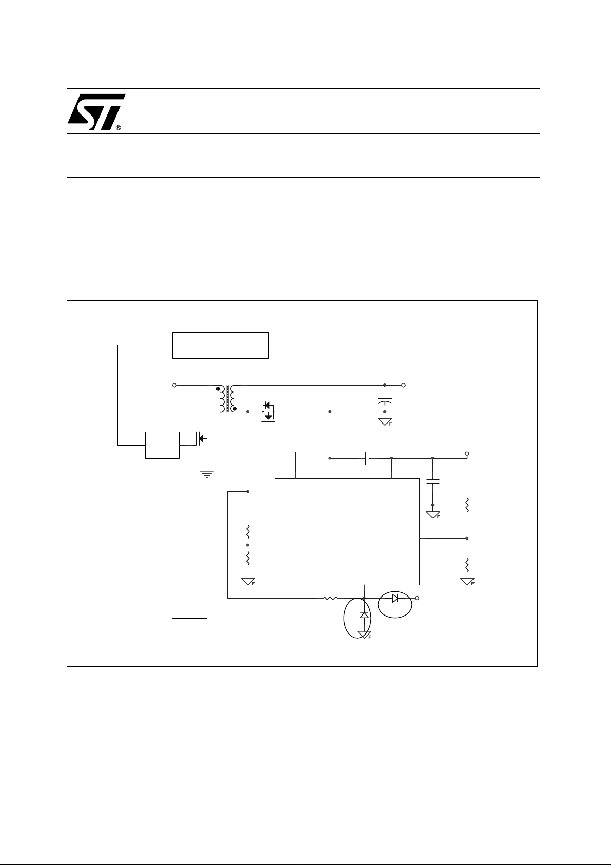
This paper describes the f unctionality and the operation of the STS R3 device used as the second ary
synchronous rectifier driver in Flyback topology switched mode power supplies. A Schematic and layout
description of a dem o board a ble to replace diode rectifica tion with synchron ous rectification in Fl yback
converters is shown below.
Figure 1: Typical Application Schematic
Feedback
Loop
TRANSFORMER
VoutVin
Cout
PWM
option
MosfetN
C1
100nF
7
R3
4
Ck
R4
OUTGate
8
PWRGND
STSR3
R5
D1
2
Vcc
SGLGND
SETANT
INHIBIT
5
D2
6
3
+5V
C2
100nF
+5V
R1
R2
January 2003
1/22
Page 2
AN1624 - APPLICATION NOTE
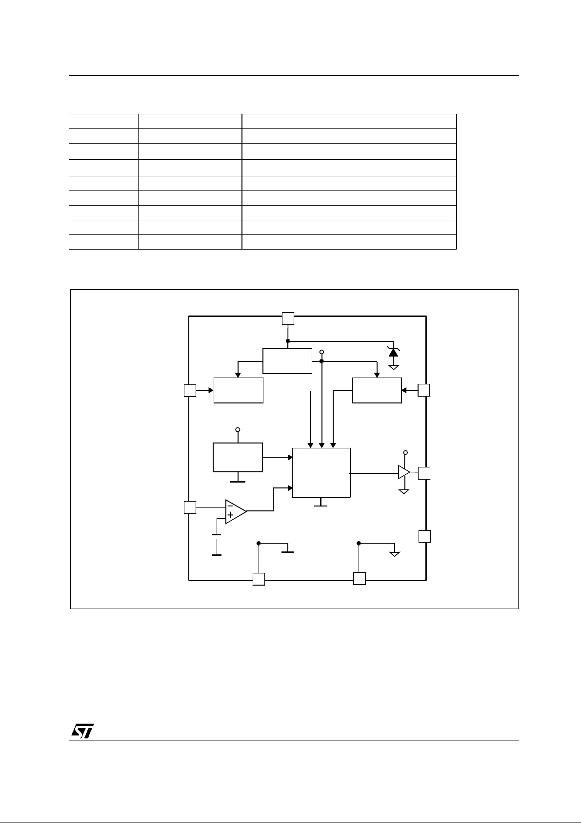
2. GENERAL DEVICE DESCRIPTION
The STSR3 Smart Driver IC provide s a high current output to properly drive secon dary Power Mosfets
used as Synchronous Rectifiers in high output current, high efficiency Flyback Converters. From a
synchronizing clock input, withdrawn on the secondary side of the isolation transformer, the IC generates
a driving signal with set dead times with respect to the primary side PWM signal.
The IC operation prevents secondary side shoot-through conditions at turn-on of the primary switch
providing anticipation in turn-off of the output. This sm art function is im plemented by a f ast cycle-aftercycle logic control mechanism, based on a hi gh frequency oscillator synchronized by the clock signal.
This anticipation is externally set through external components.
A special Inhibit function allows shut-off of the drive output by sensing the Synchronous Rectifier sourcedrain voltage and consequently turning it off when necessary. This feature makes a discontinuous
conduction mode possible and avoids reverse conduction of the synchronous rectifier in parallel
operation of the converter.
The STSR3 allows implementing Synchronous Rec tification in Discontinuous Mode PWM , Continuous
Mode PWM and Quasi Resonant Flyback Converters.
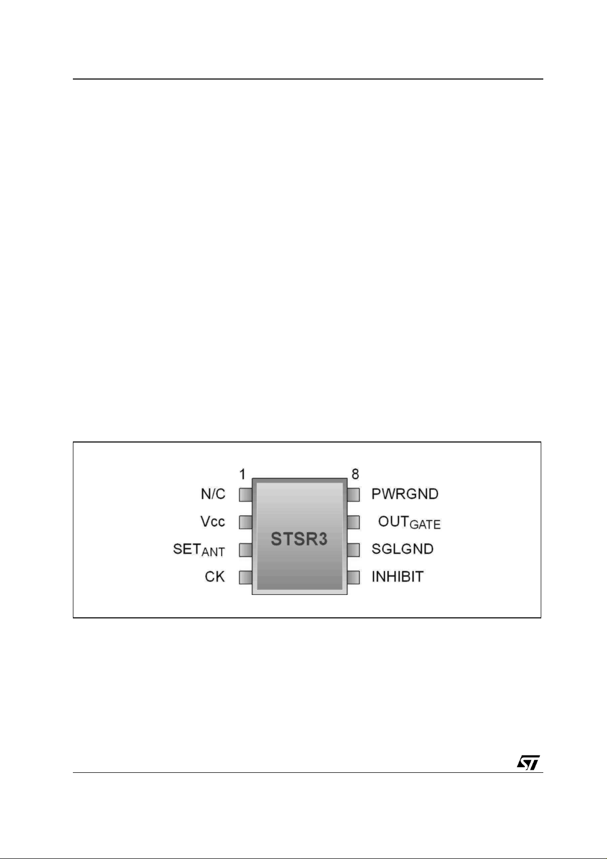
3. PIN CONNECTIONS AND DESCRIPTIONS
The STSR3 is hous ed in a n S O -8 pac kage for SMD as sembly. Device pin out is shown i n f igure 2
and table 1 briefly summarizes the device pin functionality.
Figure 2: Pin Configuration
2/22
Page 3
AN1624 - APPLICATION NOTE
Table 1: Pin Description
Pin Nu m ber Pin Name Pin Function
1 N/C Not internally connected
2 Vcc S uppl y input from 4V to 5.5V
3 SETANT Sets the anticipation in turning-off the OUT
4 CK Synchronization for IC’s operation
5 INHIBIT Discontinuous Mode Detector
6 SGLGND Reference for all the control logic signals
7 OU TG ate Output for MOSF E T G ate Dr ive
8 PWRGND Reference for power signals
Figure 3: Block Schematic
Vcc
2
2
GAT E
CK
INHIBIT
output
buffer
5.7V
3
3
7
7
1
N/C
BIAS
UVLO
4
4
5
5
Peak
detector
High
frequency
oscillator
20mV
SGLGND
DIGITAL
CONTROL
6
Anticipation
SET
86
8
PWRGND
4. SUPPLY VOLTAGE AND UNDER VOLTAGE LOCK-OUT
The supply input range is from 4V to 5.5V. An internal zener diode limits the maximum voltage to 5.8V.
A 100nF ceramic capacitor must be connected between Vcc and SGLGND pin in order to assure a stable
supply voltage. This capacitor must be placed very close to the device. Another 100nF capacitor must be
connected between Vcc and PWRGN D.
3/22
Page 4
AN1624 - APPLICATION NOTE
Under Voltage Lock Out feature guarantees proper start-up while it avoids undesirable driving during
eventual dropping of the supply voltage.
As shown in the Block Diagram, the V cc voltage also supplies also the output driver, consequently the
maximum driving voltage is 5.5V, so the use of logic gate threshold mosfets is recommended.
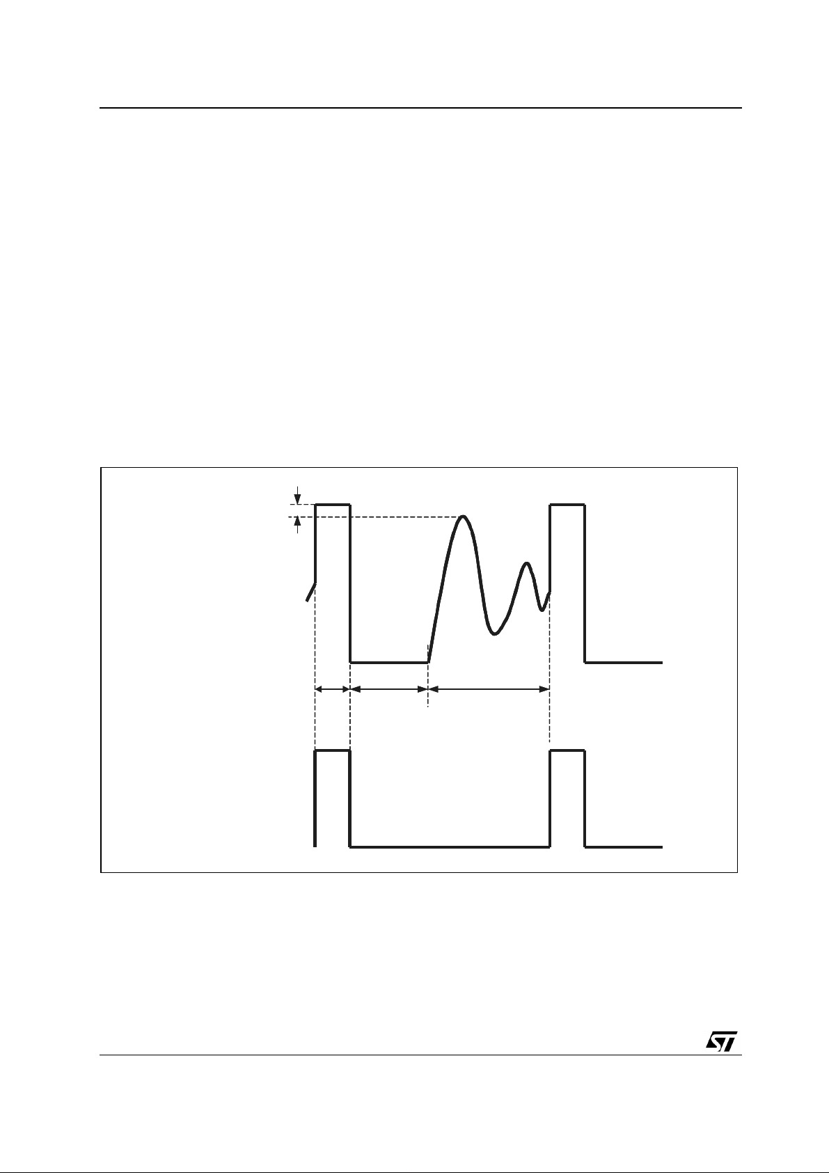
5. SYNCHRONIZATION
An innovative feature of the STSR3 is the capability to operate in the secondary side without any
synchronization signal coming from the primary side. The STSR3 synchron ization is obtained directly
from the secondary side using the voltage across the Synchron ous mosfet as the information for the
switching transitions. The Ck pin is the input for the synchronization signal; the internal threshold is set at
2.6V. As can be seen in figure 3, a Peak Det ect or is present at the in put of the Ck pin . This block is able
to distinguish between the p rimary mosfet switching transitions and the e ventual sinusoidal waveform
caused by discontinuous mode operation or resonant reset configurations (see figure 4). A wrong
synchronization causes wrong driving of the synchronous rectifier.
Figure 4: DCM waveform
V
V
1
1
Peak
Peak
Detector
Detector
Input
Input
Peak
Peak
Detector
Detector
Output
Output
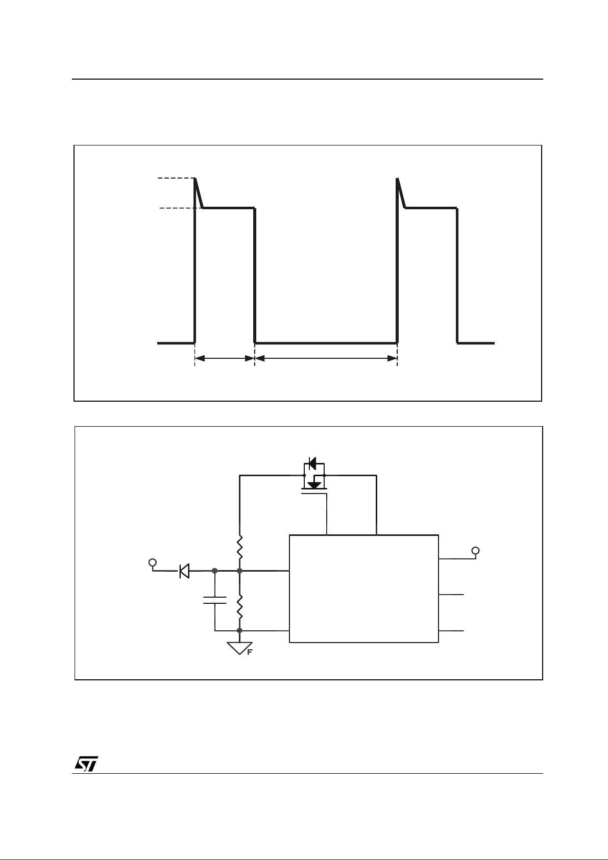
5.1 Continuous Conduction Mode
On
On
Time
Time
Off Time Dead Time
Off Time Dead Time
When the Flyback conv erter is working in continuous mode the voltage across the source and d rain of
the synchronous mosfet has a square shape. This voltage can be applied to the Ck pin using two
different configurations: with a resistor divider (figure 6) or with a diode and pull-up resistor (figure 7). In
most cases a spike is present during turn-off of the synchronous mosfet; this spike must be eliminated at
the Ck pin in order to avoid false synchronization.
4/22
Page 5
AN1624 - APPLICATION NOTE
Using the resistor divider, the spike is eliminated by adding a small capacitor (C1) as shown in figure 6.
Figure 5: CCM waveform and Ck circuit
Turn-Off
Turn-Off
Spike
Spike
On Time Off Time
On Time Off Time
Figure 6: Synchronization with a resistor divider
SYNC RECT
R1
+5V
D1
C1
R2
4
6
Ck
SGLGND
7
OUTGate
STSR3
8
PWRGND
SETANT
INHIBIT
Vcc
+5V
2
3
5
As an exam ple , in a Flybac k co nver ter fo r teleco m app licat ion , the DC inp ut vo ltage has a 1:2 variab ility
range (typically 36V-72V). Consequently, the secondary winding voltage also has 1:2 variability. The
resistor divider can be calculated in order to have about 2.8V at the Ck pin at 36V input; at 72V input, the
5/22
Page 6
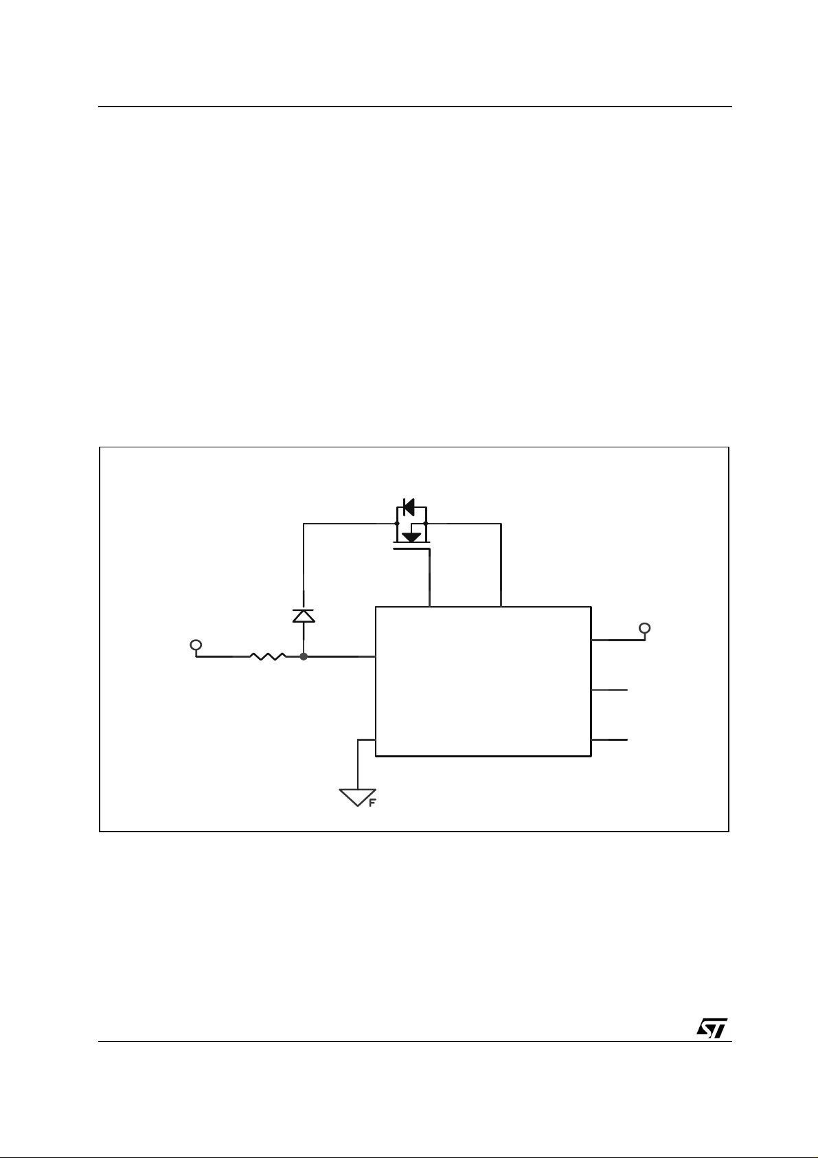
AN1624 - APPLICATION NOTE
Ck pin reaches 5.6V. Even if this value is higher than the maxim um voltage on the CK pin it can be
accepted, limiting the current flowing into the pin to 10mA.
The value of capacitor C1 is depende nt on the amount of sy nchronous mos fet turn-off spike and on the
value of R1. In order to reduce the delay introduced by R1 and C1 together , the minimum capacitor value
should be used.
In the case of an Adaptor Flyback converter , workin g with 85VAC to 270VAC input, the variabilit y range is
1:3. At the minimum inpu t voltage, 2.8V must be guaranteed at the Ck pin , consequently at maximum
input voltage, the voltage at the Ck pin will be 8.9V or higher. This voltage exceeds the absolute
maximum ratings of the device. If R1 limits the current flowing into the Ck pin to a value below the
maximum Ck current valu e indicated in the datasheet, the device can still working properly; otherwise
diode D1 must be added to protect the device.
Figure 7 shows the synchronization circuit with diode and pull-up resistor. In this case there is no
problem with the turn-off spike and maximum CK pin voltage. This circuit cannot work properly in
Discontinuous Mode due to the ringing present in the voltage drain of the synchronous rectifier.
Figure 7: Synchronization with a diode and pull-up resistor
SYNC RECT
D1
7
8
+5V
+5V
R1
4
6
Ck
OUTGate
SGLGND
PWRGND
SETANT
INHIBIT
Vcc
2
3
5
STSR3
The STSR3 can be turned off easily adding a NPN transistor between Ck and SGLGND. This transistor
forces the CK pin to GND when the signal OFF is high. In this condition the OUTGate will be in a low
state turning off the Synchronous Mosfet.
6/22
Page 7
AN1624 - APPLICATION NOTE
Figure 8 shows the turn-off circuit when using a diode and pull-up resistor to synchronize the STSR3, the
same configuration of Q1 and R2 can be used with a resistor divider circuit.
Figure 8: Shut down circuit
SYNC RECT
D1
7
8
+5V
+5V
OFF
R1
Q1
4
Ck
OUTGate
PWRGND
Vcc
SETANT
2
3
NPN
R2
6
SGLGND
INHIBIT
5
STSR3
5.2 Discontinuous Conduction Mode
As shown in figure 4, in d iscontinuous mode operat ion there can be some problems in detecting the
primary switching transitions. The internal peak detector is only able to determine the peak value
reached by the signal at the Ck pin, neglecting all signals that have a lower value. Referring to figure 4, a
minimum voltage difference V
waveform must be assured in order to allow the Peak Detector to work properly.
=400mV between the switching transition wavef orm and the sinusoidal
1
As mentioned in the previous paragraph, if the input voltage variability range is higher than 1:2, diode D1
must be added to clamp the voltage on the Ck pin. In these conditions, both switching transition
waveform and the sinusoidal waveform are clamped, and the peak detector is unable to operate correctly
causing false triggering of the STSR3 (see figure 9). In this case, using an external peak detector, like the
one shown in the next paragraph, solves the proble m.This allows correct ope ration of t he dev ice bot h i n
continuous and discontinuous mode.
7/22
Page 8

AN1624 - APPLICATION NOTE
Figure 9: DCM clamped
V
V
CC
CC
Peak
Peak
Detector
Detector
input
input
On
On
Time
Time
Peak
Peak
Detector
Detector
output
output
Off Time
Off Time
Dead Time
Dead Time
6. EXTERNAL CLOCK DETECTOR
The external clock detector is a circuit to be used when the input voltage variability is higher than 1:2.
This circuit substitutes the circuit of figure 5-6 and assures correct operation of the STSR3 both in
discontinuous and continuous conduction mode, providing a pure square waveform to CK.
R20 is a pull up resistor, when the SR mosfet is on or its body diode is conducting, the voltage V1 is low.
When the mosfet is Off (at the time of the primary switch), the voltage V1 is at 5V. R22 and C10 form a
low pass filter, which allows provision of a correct synchronized s ignal even when the ring ing is almost
zero (see Figure 11). But R22 and C10 also cause an undesired delay, so the R21 and C9 group reduce
this delay during fast swit ching transitions. The ST l ogic port 741T70 eliminates the noise, which coul d
false trigger the internal peak detector of the STSR3.
In paragraph 11 sugges ted v alues for this circuit are given.
8/22
Page 9

Figure 10: External Clock Detector Circuit
AN1624 - APPLICATION NOTE
+5V
R21
C9
C10
Figure 11: The ringing voltage near to zero can cause false trigger of the IC
R20 D14
V1
R22
+5V
74V1T70
MOSFET Drain
R23
STSR3 Ck
Mosfet Drain
Mosfet Drain
On
On
Off Time Dead Time
Off Time Dead Time
Time
Time
7. INHIBIT OPERATION
One of the differences between diode rectification and synchronous rectification is the possibility for
Mosfets to conduct the current in both directions while diodes conduct just in one direction. In
discontinuous mode with diode rectification, when the inductor c urrent reaches zero it cannot reverse
9/22
Page 10

AN1624 - APPLICATION NOTE
because the diode does not allow current flowing from c athode to anode. Using mosfets as rectifiers,
when the inductor cu rrent reaches zero, it continues to decrease becoming neg ative and flowing from
drain to source of the synchronous mosfet. In this condition the converter works as if it was in continuous
mode.
If discontinuous mode operation is required, the synchronous mosfet must be turned off when the current
is zero, consequently the body diode operates as a common rectifier, avoiding reversal of the inductor
current.
The INHIBIT pin is able to turn off the synchronous mosfet when its current is approaching zero allowing
discontinuous mode operation of the converter.
On the INHIBIT pin, there is an internal comparator with a -25mV threshold. This pin is connected
through a resistor to the drain of the synchronous mosfet. At the beginning of the off time (when Ck goes
to low level), OUTGate goes high. The INHIBIT voltage is monitored for 250ns: if the voltage on INHIBIT
is higher than -25mV, OUTGate becomes low; if the voltage on INHIBIT is lower than -25mV OUTGate is
kept high until the v oltage reaches -25m V. This is because when the sy nchronous mosfet is conducting,
the voltage on its drain is: Vds= -Rds(on)*Idrain. If Vds is hig her than -25m V, it means that the current is
decreasing and discontinuous mode is approaching, so OUTG ate is turned-off allowing operation of the
body diode of the mosfet (see figure 12). When the converter is in continuous mode the INHIBIT voltage
is always lower than -25mV and OUTGate is kept high.
During transition in which the primary mosfet is turned off, the INHIBIT vol tage must f all f rom hig h val ue
to -25mV in less than 250ns. The resistor value R26 must be chosen in order to fit this specification.
When the converter operates in parallel with other power supplies, the INHIBIT pin, detecting the voltage
across the synchronous mosfet, also avoids the converter to sink current from the output.
Figure 12: INHIBIT waveforms
SR MO SFET
SR MO SFET
source-drain
source-drain
voltage
voltage
Off Time Dead Tim e
Off Time Dead Tim e
Inductor
Inductor
Current
Current
INHIBIT
INHIBIT
Voltage
Voltage
SR MO SFET
SR MO SFET
G a t e V o lta g e
G a t e V o lta g e
-15mV
-15mV
On Time
On Time
10/22
Page 11

AN1624 - APPLICATION NOTE
Although the INHBIT pin allows operation in Discontinuous Mode, the -25mV threshold could be sensitive
to the ringing present at the SR Mosfet drain during turn off of the primary switc h, causing incomplete
turn on of OUTGat e. This inconvenience can be avoid ed using the clock signal to provide a ne gative
voltage to the INHIBIT pin act ing as a blanking time. Th is ne gat ive vol tage can be easily generated with
some discrete components as shown in figure 13.
Figure 13: Circuit to provide negative voltage to INHBIT
CK
C11
R24D15
INHIBIT
R25
Mosfet Drain
R26
The blanking time value is determined by C11 and R25. This time has to last the necessary time to cover
the ringing caused by the primary switch turn off (see Figure 14).
Figure 14: Ringing during turn off of the primary switch
11/22
Page 12
AN1624 - APPLICATION NOTE
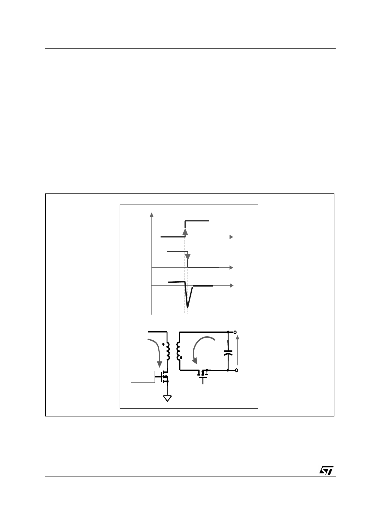
8. ANTICIP ATION
One of the maj or problems of synchronous rectification is th e generation of proper driving signals to
avoid cross conduction between the Synchronous rectifier and the primary switch.
Referring to figure 15, when the primary Mosfet is turned-on, t he voltage Vs tends to go negative. If the
synchronous mosfet is turned off with some delay, a short circuit loop between primary side and
secondary sides o ccurs. In order t o avoid this undesired condition, the s ynchronous mosfet must be
turned off before the primary mosfet is turned on; this means th at a certain amount of ’anticipation’ is
needed.
Figure 16 shows the detailed timing of Ck and O UTGate signals in normal operation. Time interval t
provides the required anticipation to avoid any short circuit con dition. For t
it is possible to choose
ant
between three different values using the SETAnt pin according to table 2:
Figure 15: Short circuit in the secondary side
Primary
Primary
Mosfet ON
Mosfet ON
VS
VS
t
t
VGS(SR)
VGS(SR)
t
t
I
I
SR
SR
t0
t0
t1
t1
t
t
ant
12/22
PWM
PWM
SR
SR
VOUTVs
VOUTVs
Page 13
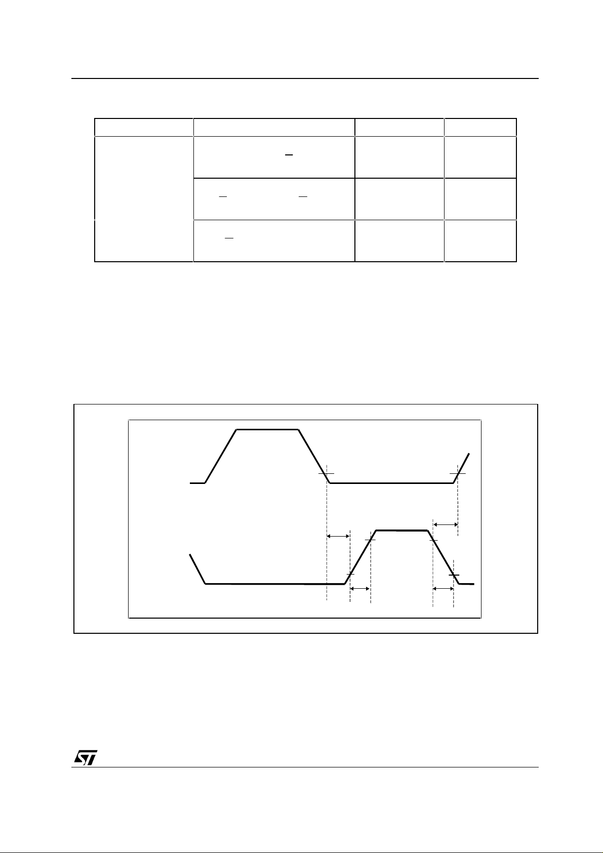
Table 2: Anticipation values
Parameter Condition Value Unit
AN1624 - APPLICATION NOTE
0<SETAnt<
1
Vcc
75 ns
3
tant
1
3
Vcc
2
Vcc
<SETAnt<
< SETAnt<Vcc
2
3
Vcc
150 ns
225 ns
3
The voltage on the SETAnt pin can be obtained using a resistor divider of the supply voltage (see Table
2).
The Digital Control Block generates these anticipations by counting the number of high frequency pulses
included within the switching period. Due to the digital nature of this system, some bits can be lost during
the counting, causing a jitter in the output driving signal. The value in the table is an average value, which
takes into account this jitter. Figure 17 shows the jitter during turn off of OUTGate.
Figure 16: STSR3 Timing
CK
OUT
Ant
Tp2
GATE
Tr Tf
13/22
Page 14

AN1624 - APPLICATION NOTE
Figure 17: OUTGate turn off Jitter
9. NO LOAD AND LIGHT LOAD OPERAT IO N
When the duty-cycle is lower than 14%, an internal feature of the STSR3 allows a total shutdown of
OUTGate and of most inte rnal parts of the device, causing a reduction in power consum ption. In these
conditions the low output current of the converter is carried by the body diode of the mosfet. The IC starts
to operate again when the duty-cycle is higher than 18%, therefore having a 4% of hysteresis. This
feature allows correct operation when primary the PWM controlle r imposes burst mode due to the very
light output load.
10. OUTPUT DRIVERS
The output driver has a high current capability, being able to source up to 2A and to sink up to 3.5A peak
current. Consequently, the synchronous mosfet is switched very quickly, allowing paralleling of several
mosfets to reduce conduction losses. The high level driving voltage is equal to Vcc voltage; therefore the
device drives only mosfets with logic level gate thresholds.
14/22
Page 15

Figure 18: Rds(on) source/sink vs Temp
1.4
1.4
1.2
1.2
1
1
]
]
Ω
Ω
0.8
0.8
0.6
0.6
Rds on [
Rds on [
0.4
0.4
0.2
0.2
0
0
-40 -20 0 20 40 60 80 100
-40 -20 0 20 40 60 80 100
Source
Source
Sink
Sink
T [ °C]
T [ °C]
AN1624 - APPLICATION NOTE
11. TRANSIENT BEHAVIOR
During very heavy load changes, the duty cycle can vary very fast from a low value to high value and vice
versa in a few switching periods.
Being the anticipation time for OUTGate based on the calculation of the switching period (frequency) and
not on duty cycle, even during fast duty cycle changes the anticipation t ime is provided correctly, always
providing correct driving for the Synchronous Mosfet.
Figure 19a: Duty Cycle very fast variation
5 µs
5 µs
5.0 V
5.0 V
CK
CK
5 µs
5.0 V
OUTGate
33.0 µs
15/22
Page 16

AN1624 - APPLICATION NOTE
@ 5V (m
Figure 19b: Duty Cycle very fast variation
1 µ s
1 µ s
0.47 V
0.47 V
CK
CK
1 µ s
1 µ s
-4.38 V
-4.38 V
OUTGate
OUTGate
53.6 µ s
53.6 µ s
∆ t 131.5 ns
∆ t 131.5 ns
1
1
/
7.605 MHz
/
7.605 MHz
∆ t
∆ t
Figure 19a shows the condition in which the duty cycle passes from 50% to 80% in one cycle and back to
50%. OUTGate is provided correctly, and in figure 19b the anticipation time of 131ns is shown.
12. DEMOBOARD DESCRIPTION
The schematic of figure 20 presen ts a test board for the STSR3. This board replac es the diode in a
Flyback converter and includes all the components needed by the STSR3 to operate, plus the
synchronous mosfet. Synchronization is obtained with the external clock detector making the board
usable in every kind of Flyback converter, both AC/DC and DC/DC. Some parts of the circuit shown in
fig.20 might not be necessary depending on the kind of the application. For example if there is no ringing
at turn-off of the primary switch, the components R24, D15, R25 and C11 can be omitted.
A Synchronous Mosfet in the TO220 package can be mounted on board. ST provides suitable
Synchronous Mosfets for this application:
P/N VD
STP100NF03L-03 30 4.5 100
STP80NF03L-04 30 5 80
STP90NF03L 30 12 90
STP85NF3LL 30 9 85
STP70NF3LL 30 12 70
STP100NF04L 40 5 100
STP80NF55L-06 55 8 80
STP60NF06L 60 16 60
STP80NF75L 75 13 80
STP40NF10L 100 36 40
(V) RDS
SS
(on)
) I
Ω
D(cont)
(A)
16/22
Page 17

AN1624 - APPLICATION NOTE
The board allows us to easily pass from diode rectification to synchronous rectification in Flyback
converter applications. Table 3 shows detailed components selection.
Figure 20: Demo board Schematic
+5V
C9
C10
R20
R21
C11
R22
+5V
U3
D15 R24
R25
R26
74V1T70
+5V
D14
R23
CON1
D16
+5V
CON2
7
R4
R19
OUTGate
STSR3
C8
8
PWRGND
c
PWRGND
SGLGND
SETANT
Vcc
CON4
c
Vout
JP1
3
VI
C2
78L05
C5
2
6
3
C6
D10
JP4
Vo
GND
2
R7
JP5
R13
+5V
1
C3
JP6
c
C1
R1
D1
M1
D13
D2
U2
4
Ck
5
INHIBIT
D7
17/22
Page 18

AN1624 - APPLICATION NOTE
Table 3: Demo Board Components
Compone nt Notes
Supply
C5, C6
U1
C2 78L05 input capa citor (330nF ceramic)
C3 78L05 output capacitor (150nF ceramic)
D10 P rotects Vcc from voltages higher than 5.6V
JP1 Close this jumper if a 5V is already available on the board
Synchr onization
D2 Protects Ck pin from voltages higher than Vcc (not necessary if U3 is used)
D14 Blocks the high voltage coming from the SR Drain
R20
R21
R22
R23
C9 Speed up capa citor (22pF)
C10 Low pass filter capacitor (10pF)
U3 Non Inverting Buffer ST 74V1T70
INHI BIT
R26 Limits the current to diode D16 when SR Drain voltage is higher than Vcc
D16
D7 Protects INHIBIT pin from negative voltages.
D15 Prevents C11 to be discharged
R24 Blank ing circuit summing resistor
R25 Blank ing Time resistor
C11 Blank ing Time capacitor
Anticipation
R7, R13
JP6 Sets the maximum anticipation time
JP5 Sets the medium anticipation time
JP4 Sets the minimum anticipation time
Power
M1 Synchronous Mosfet TO220
R4 Gate pul l down resistor
R19
C8 Gate capacitor to avoid dv/dt turn-on of the SR Mosfet (Not ne cessary in common application))
D13 Speed up turn-off of SR Mosfet if R19 is used.
D1
C1, R1 A small snubber reduces synchronous Mosfet turn-off spike
Vcc bypass capacitors
100nF ceram ic
Standard voltage regulator to p rovide 5V supply voltage (SOT89). Omit this component and close
jumper JP1 if 5V is already present on the board
L78L05ACU
Pull–up resistor (3.3kΩ)
Speed up resistor (10kΩ)
Low pass filter resistor (10kΩ)
Ck series resistor (1kΩ)
Protects INHIBIT pin from voltages higher than Vcc. Not nece ssary if the current flowing into
INHIBIT pin is less than 10m A.
Resistor divider which provides voltage level to set Anticipation time
R7=R13= 10kΩ
Gate series resistor (Typically 0Ω)
A Schottky Rectifier in parallel to synchronous mosfet can increase convert er efficiency due to low
drop voltages during Gate drive dead time
18/22
Page 19

AN1624 - APPLICATION NOTE
13. PCB LAYOUT
Any Switch Mode Power Supply requires a good PC B (Printed Circuit Board) design layout in order to
achieve maximum performance in terms of system functionality and emitted radiations. Component
placing, traces routing and width are the major issues. Some fundamental rules will be given so that the
PCB designer can produce a good layout for the STSR3
All traces carrying current should be drawn on the PCB as short and thick as possible. This should be done
to minimize resistive and induc tive paras itic effect s, gaining in system efficiency and radiated emissions.
Current return routing is another crucial issue. Signal ground (SGLGND) and power ground (PWRGND)
must be routed separately and connected to a single ground point.
The INHIBIT pin, due to the -25mV comparator could be sensitive to layout, so make the INHIBIT
connection as short as possible.
As a rule of thumb, traces carrying signal currents should be placed far from traces carrying pulsed
currents or quickly swinging voltages avoiding any coupling effect between them.
Figure 21a: Board Layout - Components (two times actual size)
19/22
Page 20

AN1624 - APPLICATION NOTE
Figure 21b: Board Layout - Top Side (two times actual size)
Figure 21c: Board Layout - Bottom Side (two times actual size)
20/22
Page 21

AN1624 - APPLICATION NOTE
14. HOW TO USE THE BOARD
The demo board is meant t o implement synchronous rec tification in a Flyback converter. If the diode is
mounted on the board, it must be rem ov ed. Connect the Demo Boa rd as depict ed i n f igure 22. If Vout is
equal or higher than 5V connect Vs to Vout (as in the figure 22). If Vout is lower than 5V, connec t Vs
together with FW Drain.
Figure 22: Connecting the Demo Board
Feedback
Feedback
Loop
Loop
Vs
Vs
VoutVin
VoutVin
PWM
PWM
Drain
Drain
PWRGND
PWRGND
15. CONCLUSION
A new device for controlling synchronous rectifiers in high efficiency AC/DC and DC/DC Flyback
Converters is presented. The device is completely transparent to the primary PWM controller, and it
works in the secondary side requiring no interaction with the primary side. The device is able to operate
with any kind of topological configuration providing the correct driving signal for the synchronous
MOSFET.
The presented board allows implementation of synchronous rectification in any existing Flyback
converter in an easy and effective way.
21/22
Page 22

AN1624 - APPLICATION NOTE
Information furnished is b elieved to be accurate a nd reliable. Howe ver, ST Microelectronics a ssumes no resp onsibility
for the consequences of use of such information nor for any infringement of patents or other rights of third parties
which may result from its use. No license is granted by implication or otherwise under any patent or patent rights of
STMicroelectronics. Specification ment ioned in this p ublication are subject to change without notice. This publication
supersedes and repla ces a ll information pre viously su pplied. STM icr oelectro nics pr oducts are not authorized for use
as critical components in life support devices or systems without express writt en approval of STMicroelectronics.
The ST logo is a registered trademark of STMicroelectronics
© 2003 STMicroelectronics - Printed in Italy - All rights reserved
Australia - Brazil - Canada - China - Finland - France - Germany - Hong Kong - India - Isreal - Italy - Japan - Malaysia -
Malta - Morocco - Singapore - Spain - Sweden - Switzerland - United Kingdom - U.S.A.
22/22
STMicroelectronics GROUP OF COMPANIES
http://www.st.com
 Loading...