

Page 1

AN1620
APPLICATION NOTE
25W OFF-LINE AUTORANGING BATTERY CHARGER
WITH L5991A
by Domenico Arrigo
INTRODUCTION
This note describes an off-li ne autor anging (85Vac- 264Vac) batter y charge r designed to oper ate i n three different functional modes:
– constant voltage
– constant current
– constant power
These requirements are typical of battery chargers for notebook computers.
The resulting output characteristic of the system is shown in fig 1.
The A-B portion of the V-I characteristic is a constant voltage mode. This situation happen when the battery
pack is almost co mpletely charged. V o has to be set at the final v alue of the battery pack. From point B to C the
charger operates in constant power mode, reducing the output voltage while increasing the output current.
The benefit of introducing the constant power mode is that the maximum output power is lower with respect to
the power output at point E. This reduces the power managed by the primary circuitry and in consequence reduces the total dissipation power. This is a useful improvement considering that the complete system is packaged in a plastic case with a very limited capability of dissipating heat.
From point C to D the adapter works in constant current mode until the output voltage reaches 0V.
In practice it is difficult to have a constant current characteristic below an output voltage of 2-3V because the
primary auxiliary supply voltage drops at the controller turn-off threshold (internally fixed at 7.6V typ.) and the
V-I characteristic exhibit a foldback to zero.
If mandatory to operate in constant current mode till 0V, a secondary post-regular or other tricky solutions on
the windings, primary or secondary, are required.
Fig 2 shows the V-I characteristic obtained with the circuit of Fig 3.
ELECTRICAL SPECIFICATION:
Input voltage 85Vac to 264Vac
Regulated output voltage 18V
Maximum output power 25W
Switching frequency 100kHz
Target efficiency @ full load >80%
Topology discontinuous current mode flyback
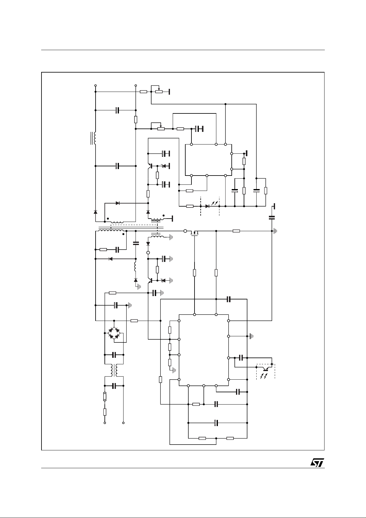
Fig 3 shows the electrical circuit.
Figure 1. V-I output characteristic Figure 2. Practical V-I characteristics
V
ABE
November 2002
D96IN437
C
DI
V
O
15
Vin=110V
10
5
0
0 0.5 1.0 1.5 2.0 I
Vin=220V
AC
D96IN439
AC
O
1/4
Page 2
AN1620 APPLICATION NOTE
Figure 3. AC-DC converter electrical schematic
25W
18V/2A
20K
R18
L2 5µH
C13
D7 STPS8H100D
T1
C14
2 x
D11
5T
R16
R17
40m
330µF
470µF
Q4 BC337
R12 10K
R14 82D6
3T
R22
4.7K
1K
C15
D8
C18
22µF
9V
1µF
R21
12K
REF
V
R19
R13
1
8
13K
240
C2
1µF
Crin
Vrin
537
GND
4
6
OUTPUT
C16 220nF
2
CREF
C
R24
R25
2.2K
C17 220nF
TSM
101A
2
CC
V
Csen
1
IC2
IN537_mod
R23 100K
C18 2.2nF
41T
C1
50pF
10K
R20
D4
STTH1L06
R1
91K
0.5W
C4
82µF
400V
B1
-+
C3C0
LF
FUSE
THERMISTOR
Vac
85 264
C5 120pF
L1
470µH
D3
STTH1L06
R28
2.7M
D2
R4 20K
Q3 BC337
C6
6T
22µF
R3 10K
C7
22µF
D5
18V
R26 10R10 36K
R9 5.1K
C
V
CC
V
DISDCC
Q1
STP4NL80Z
9814
3
4
R6 10
OUT
10
REF
V
R05
L5991A
2
RCT
10K
R7
5.1K
R30 1K
ISEN
13
7
SS
C10
2.2nF
C9
1µF
0.5
R29
C8
100pF
11
12
SGND PGND
1nF
C12
6
5
COMP
5
FB
C11
10nF
R8
5.1K
TCDT
1101GB
4
IC2
2/4
Page 3

AN1620 APPLICATION NOTE
The realisation of the three different functional modes requires dedicated controls.
The voltage and current controls are located on the secondary side of the transformer, and the error signal is
transferred to the primary controller via an optocoupler in order to have an isolated feedback.
The TSM101A a dual op/amp, with an internal 1.24V reference is used. One op/amp is dedicated to the v oltage
mode control and the second one to the constant current control.
The two output are OR-ed and the common point drives the optocoupler.
The current signal is taken across the 40mOhm current sense resistor, R16, while the R18 potentiometer ad-
justs the output voltage.
The constant power char acteristic is easy to achi eve with di scontinuous mode operation, since constant primar y
peak current means constant output power. The value is programmed by adding a proper offset voltage, defined
by R3 value (fig 4), to the current sense ramp at pin 13.
Figure 4. Schematic diagram for output constant power.
2.7M
10
1K
100pF
IN438_mod
0.5Ω
L5991A
4
10K
10
13
The value of this resistor is related to the desired output power Pout by the below relationship:
R
where L1 is the primary inductance,
----------------------------------------------------------------------- -
⋅=
R
3
30
η
is the expected efficiency, f is the switching frequency and Rs is the cur-
--------------------
1
L
4
2
⋅⋅–
η⋅⋅
f
1
P
R
S
out
rent sense resistance.
The L5991A introduces a delay, td @ 100ns, at turn-off, on the current loop, and due to this, the primary peak
current value increases according to its slope.
The consequence is that the regulated output power is a function of the input voltage. R28 is introduced in order
to compensate this error.
Its value can be calculated with the following formula:
()
R30/ /R
28
------------------------------------- -=
t
R
⋅
3
⋅
R
d
S
L
1
A primary auxiliary winding is r equired to suppl y the IC after turn- on, and it has to be designed to generate a dc
voltage within the limits of the IC supply v oltage range. It shoul d be loosely coupled w ith the secondar y winding
in order to minimise the reflected secondary-to-primary effects when the output voltage is going down towards
short circuit.
A second auxiliary winding, on the secondary side transformer, forward coupled with the princi pal primary winding, has been ad ded. When the sys tem is in constant curr ent mode, and the output voltage is re duced, this winding provides the supply voltage for the TSM101A.
The Table A summarises the efficiency performance of the complete system, and Table B shows the electrical
system performance.
3/4
Page 4

AN1620 APPLICATION NOTE
Table A. System efficiency.
Vin (Vac) Iout = 1A Iout = 2A, Pout = 36W Iout = 1.8A, Pout = 25W
85
110
220
264
Vout (V)
17.97
17.94
17.89
17.89
η
83.9%
85.1%
84.4%
82.0%
Vout (V)
17.96
17.96
17.91
17.89
η
82.2%
83.7%
83.5%
83.0%
Vout (V)
13.82
13.86
14.31
14.41
Table B. System performance (Pout limited to 25W)
Line regulation Vin = 85 to 264 Vac, Iout = 1A 80mV
Load regulation Iout = 0.5 to 1.8A, Vin = 85V
Vin = 264V
Maximum efficiency Vin = 180 Vac, Iout = 1.8A 85.2%
Output ripple Vin = 85 to 264 Vac, Iout = 1.8A < 200mV
10mV
10mV
η
82.6%
83.7%
83.8%
82.7%
Information furnished is believed to be accurate and reliable. However, STMicroelectronics assumes no responsibility for the consequences
of use of such information nor for any infringement of patents or other rights of third parties which may result from its use. No license is granted
by implic ation or otherwise under any patent or patent r i ght s of STMi croelectr oni cs. Specifications menti oned in thi s publication are s ubj ect
to change without notice. This publication supersedes and replaces all information previously supplied. STMicroelectronics products are not
authorized for use as cri tical components in li f e support dev i ces or systems without express writ t en approval of STMicroel ectronics.
The ST logo is a registered trademark of STMicroelectronics
© 2002 STMic roelectroni cs - All Rig hts Reserv ed
Australia - Brazi l - Canada - Ch i na - F i nl and - France - Germany - Hong Kong - India - Israel - Italy - Japan -Malaysia - Malta - Morocco -
Singap ore - Spain - Sw eden - Switzerland - U ni t ed Kingdom - United St at es.
STMicroelectronics GROUP OF COMPANIES
http://www.s t. com
4/4
 Loading...