

Page 1

AN1608
®
CHECK THE ROBUSTNESS OF CLT3-4BT6
CONTENT
DESCRIPTION OF THE CLT3-4BT6 PRODUCT
■
CLT3-4BC6 DEMONSTRATION BOARD
■
EMC REQUIREMENTS
■
ROBUSTNESS AND IMMUNITY OF THE
■
CLT3-4BT6 DEVICE
CONCLUSION
■
REFERENCES
■
1. DESCRIPTION OF CLT3-4BT6 PRODUCT
1.1. Functional description
TheCLT3-4BT6(CurrentLimitedTermination)isa
quadruple input digital termination device
designed for 24V DC automation applications. It
achieves the front-end circuitry of a digital input
module (I/O) in industrial automation.
Available in a four channels configuration, it offers
a high-density termination by minimizing the external component count. It is housed in a TSSOP20
surface mount package to reduce the printed
board size.
Made of a parallel input voltage protection, aserial
input-output current limiting circuit and an
opto-coupler driver, each channel circuit
terminates the connection between the logic input
and the associated high side sensor or switch.
The CLT3-4BT6 device is used between the sensors and the opto-coupler of an input module. The
current limiting circuit, connected between the input and the output pins, is compensated all over
the temperature range. Furthermore, each channel runs independently of the other. Thanks to its
low tolerance, the current limitation allows the
drastic reduction of the dissipation compared to a
resistive input: the overall module requires less
cooling capability and becomes smaller.
The output block of each termination channel
controls the operation of an opto-coupler that is
internally enabledbyaLightEmittingDiode.When
the input current is less than 1.5mA, an integrated
APPLICATION NOTE
CLT3-4BT6 DEMOBOARD:
output circuit derivates the input current to
maintain the opto-coupler off.
When the CLT input voltage V
(that corresponds to a module input voltage higher
than 11V with a 1.2kΩ serial resistor), a minimum
output current of 1.5mA secures the opto-coupler
in the on state.
The CLT3-4BT6 protects the input module against
transient electromagnetic interferences such as
those described in the IEC61131-2 standard.
The opto-coupler plays a role in the CLT3-4BT6
operation. The drop voltage of its input diode
introduces a voltage offset in series with the
CLT3-4BT6 channel: for a good CLT3-4BT6
operation, this drop voltage should remain below
2V (see
CLT3-4BT6 datasheet
1.2. Application requirements
A reverse blocking diode is connected between
the module ground connection and the common
pin COM of the CLT3-4BT6 device to protect the
module against spurious reverse supply
connection. This diode also protects the
CLT3-4BT6 device against negative surge
voltages.
An external output capacitor is placed either at the
input or the output of the CLT3-4BT6 to filter the
transient disturbances injected in the inputs of the
module and secure the immunity of the module
itself.
All immunity requirements are described by the
IEC61131-2 international standard.
is higher than 5V
IN
for more details).
October 2002 - Ed: 1
1/7
Page 2
APPLICATION NOTE
2. CLT3-4BT6 DEMONSTRATION BOARD
2.1. Description of the CLT3-4BT6 demoboard
This CLT3-4BT6 demonstration board allows the
evaluation of the function of the CLT3-4BT6
product. It can be easily inserted in a real
application, between sensors and digital bus
controller. The output LEDs give the state of each
line of the CLT3-4BT6, according to the state of
each input.
ThePCBofthedemonstration board hasthe structure described by the
figure 1
. It has been de-
signed and optimized with the components
table 1
presented in the
. This configuration gives a
good example of a robust interface design.
Table 1: bill of material.
Reference Nb Part description Package
J1, J2 2 Connector 6 pins 2.54 pitch
Rin1, Rin2,
4 1.2 kΩ, 0.25 W 1206
Rin3, Rin4
RC 1 4.7 kΩ, 0.33 W 1206
C1, C2, C3,C44 22 nF, 60 V 1206
R_LED 1 4 resitors array
1206
330Ω, 0.13W
LED1, LED2,
4 LED 10 mA 1206
LED3, LED4
U1 1 CLT3-4BT6 TSSOP20
U2 1 TLP281-4 SO-16
The copper surface under the CLT device improves the thermal dissipation capability of the
TSSOP20 package. The copper area on the PCB
demoboard is around 1.2cm², and makes it possible to decrease the Rth of the package to a value
lower than 100°C/W.
2.2. Operating instructions of the CLT3-4BT6
demo-board
This paragraph provides some basic advices to
implement properly the demonstration board in order to evaluate the CLT3-4BT6 product.
■
Inputs / Outputs
The input connector gives access to the 4 input
signals of the module (In1, 2, 3 and 4), and the
power supply access of the CLT3-4BT6 (Vcc and
Com). It is then easy to connect this module directlyto any type ofsensor, especially those specified by the EN60947-5-2 standard.
Theoutput connector givesaccess to the4 outputs
of the module (output of the opto-coupler, Out1, 2,
3 and 4). Furthermore, this connector is also used
to connect the output power supply (Vcc2 and
Com2). It is then easy to connect the output of the
module directly on a digital bus controller.
Power supply
■
- Vcc power supply
The Vcc power supply shall be a 24Vdc voltage
supply. Actually, the CLT3-4BT6 device needs a
10 to 30Vdc voltage to work.
- Vcc2 power supply
The output power supply can be a 5Vdc voltage
supply. This voltage supplies the 4 collectors of
each opto-coupler output.
NOTE: Do not short the opto-coupler output to
ground. This may result in the destruction of the
output transistor of this opto-coupler.
Discrete components
■
- Discrete capacitors:
Some 22nF capacitors are used in order to improve the noise immunity of the whole module and
to filter the high frequency electrical noise in the off
state.
They can be placed at the output of the CLT (betweenthe CLT device and the opto-coupler) as described in the
datasheet
. This configuration meets
the minimum level of immunity described in the
IEC61131-2 standard. The configuration corresponding to capacitors placed at the input of the
CLT device (between input resistors and the CLT
device), as in the demonstration board topology,
allows an increase of this immunity. However, the
normal operation of the module remains within
specification whatever the position of the capacitors is.
- Input resistors:
The input resistors are used in order to limit the
current that could appear in case of voltage surge
clamped by the CLT3-4BT6. These resistors shall
then withstand the high overvoltage that may be
applied to the module during surge tests.
- LEDs resistors:
The value of these resistors shall be set according
to the input power supply value used, and the normal current of displaying LEDs. A resistor array
can be used to control these low power LEDs (reducing of the PCB size).
- Diode D1:
The diode used between the COM of the input
power supply, and the COM of theCLT3-4BT6 device can be a general purpose component as a
1000V 1A rectifier.
■
Opto-coupler
The opto-coupler should be chosen according to
its input diode drop voltage and should fit the wide
range output voltage of the CLT3 output (0.2V).
2/7
Page 3
APPLICATION NOTE
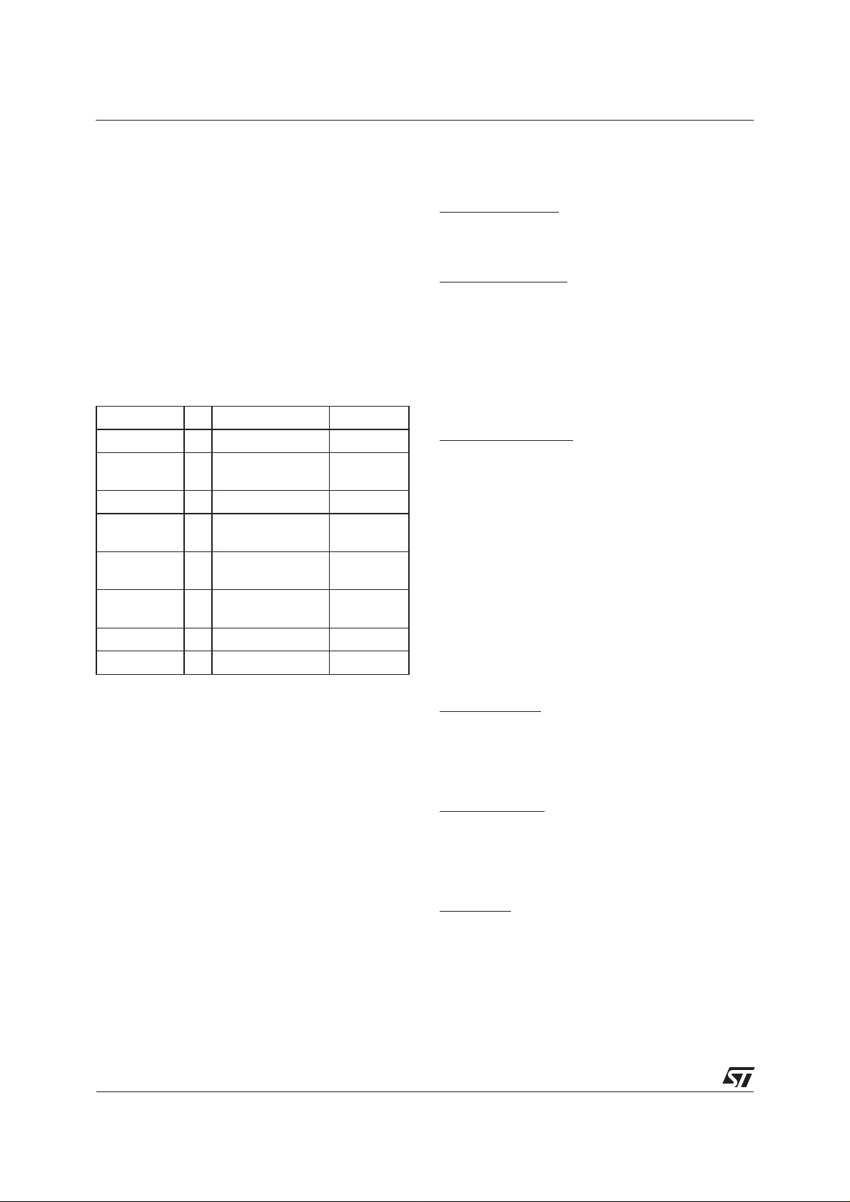
Fig. 1: Electrical diagram of the CLT3-4BT6 demonstration board for reinforced EMC.
Vcc2
16
C1
15
E1
14
C2
13
E2
12
C3
11
E3
10
C4
9
E4
Vcc
Vcc
RC
4.7k
U1
1
COM
C4
22nF
2
In1
3
ESD12
4
IN2
5
Vc
6
ESDc
7
In3
8
ESD34
9
In4
10
COM
CLT3-4
Input
1
2
3
4
5
6
J1
Rin1
1.2k
Rin2
1.2k
Rin3
1.2k
Rin4
1.2k
D1
C1
22nF
C2
22nF
C3
22nF
COM
Out1
COM12
Out2
COM
COM
Out3
COM34
Out4
COM
20
19
18
17
16
15
14
13
12
11
U2
1
2
3
4
5
6
7
8
A1
K1
A2
K2
A3
K3
A4
K4
Opto-coupler
45
678
Output
1
2
Vcc2
3
4
5
6
J2
123
R_LED
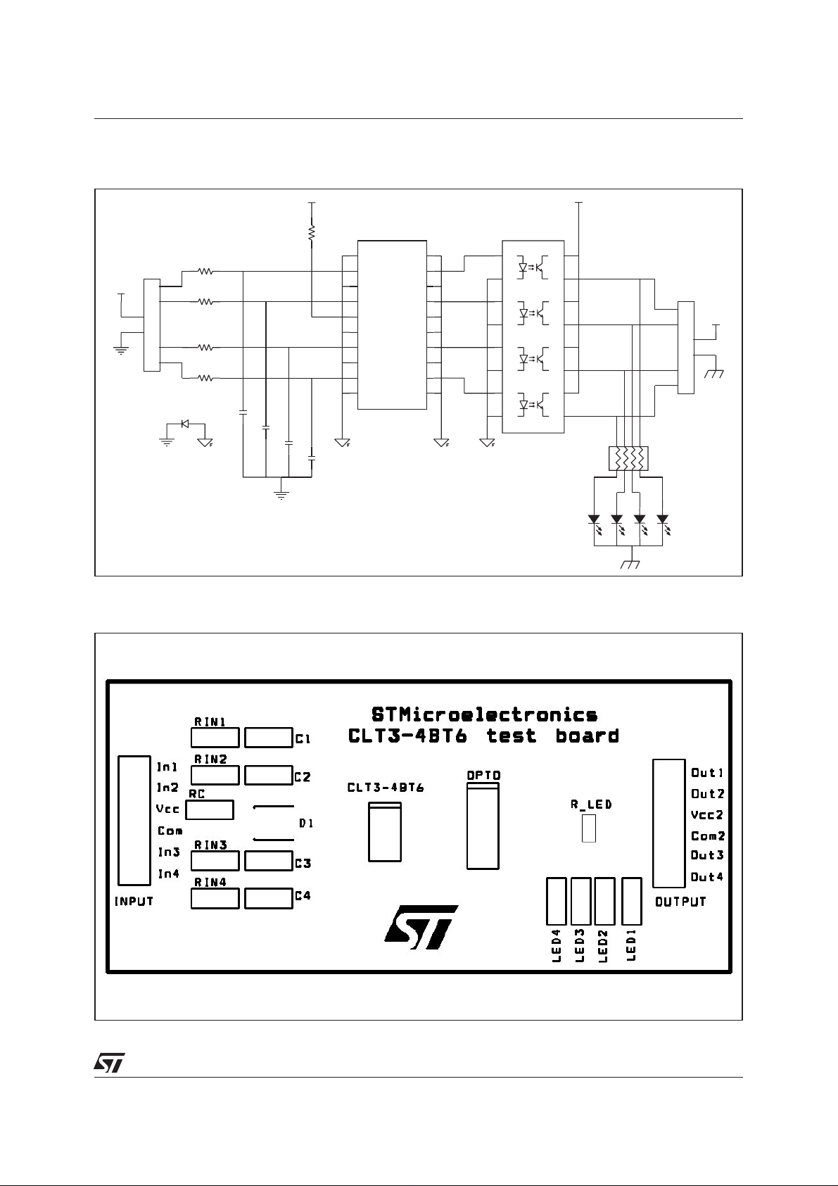
Fig. 2: Assembly top view of the demonstration board.
LED4
LED1
LED2
LED3
3/7
Page 4

APPLICATION NOTE
3. EMC REQUIREMENTS
3.1. Description of the procedure to evaluate
the robustness of the CLT3-4BT6
The reference to evaluate the robustness of the
CLT3-4BT6 product is the IEC61131-2 international standard. This international standard gives
all requirements and conditions of tests that must
be performed on the programmable logic controllers PLC and their associated peripherals.
Thispaper focuses on the most stressfully tests for
the CLT3-4BT6 product. The immunity of the
CLT3-4BT6 is tested according to the standards.
The IEC61131-2 standard specifies the
Electromagnetic Compatibility (EMC) requirements
and the nature of the tests to perform in order to
determine if the system meets these requirements
paragraph 7: "EMC requirements" and paragraph 8:
(
"EMC type tests and verifications" of the Ed2 of the
standard
). The levels of each test depend on the zone
where the system will be installed. The most typical
industrial environmental levels correspond to zone B:
local power distribution zone and dedicated power
distribution zone (
of the IEC61131-2-Ed2 standard
see table 28: "EMC immunity zones"
). The following
paragraphs recall the test levels for this zone.
3.4. Surge test (according to the IEC61000-4-5)
Since the voltage surge consists in a single but energetic pulse, the CLT3-4BT6 device embeds an
over-voltage protection on each point. The absorbed energy complies at least with the requirements of the IEC61131-2 standard. The high
energy surge test must be applied on all input pins
of the system. For all analog inputs, the coupling
method is a 47Ω serial resistance and a 0.5µF capacitor.For dc power line, thecoupling is 2Ω, 18µF
with differential mode, and 12Ω, 9µF with common
mode.
The required voltage surge levels are:
analog or dc I/O: 0.5kV (line to line and line to
■
earth coupling modes),
dc power line: 0.5kV (line to line),
■
dc power line: 1kV (line to earth).
■
The PLC system shall continue to operate as intended. Temporary degradation of the performance is acceptable during the test, but the
system must recover by itself after the test (
rion according to the IEC61131-2 standard
B crite-
).
3.5. Conducted disturbance tests (according to
the IEC61000-4-6)
3.2. ESD tests (according to the IEC61000-4-2)
The electrostatic discharge test shall be applied to
operator accessible devices. This means that these
tests have to be performed on each connector pin.
The required levels are:
■
air discharge: +/-8kV
■
contact discharge: +/-4kV
The PLC system shall continue to operate as intended. Temporary degradation of the performance is acceptable during the test, but the
system must recover by itself after the test (
rion according to the IEC61131-2 standard
B crite-
).
3.3.Burst tests (according to the IEC61000-4-4)
Thefast transient burst tests must be applied on all
the input pins of the system. A capacitive
clamp-coupling device (50-200pF) must be used
as described in the IEC61000-4-4 standard.
The required burst voltage levels are:
■
analog or dc I/O: +/-1kV,
■
dc power line: +/-2kV.
The PLC system shall continue to operate as intended. Temporary degradation of the performance is acceptable during the test, but the
system must recover by itself after the test (
rion according to the IEC61131-2 standard
B crite-
).
The conducted radio frequency interference test
mustbe applied onall input pinsof the system.The
frequency range is 150kHz to 80MHz, with a 80%
amplitude modulation by a 1kHz sinusoidal wave.
A CDN (Coupling Device Network) or a current
coupling clamp (as described in the IEC61000-4-6
standard) has to be used to apply the stress to the
system.
The required level is:
■
3Vrms, whatever the tested system input is.
The PLC system shall continue to operate as intended. No loss of function or performance is acceptable (
IEC61131-2 standard
"A" criterion according to the
).
3.6. Reverse analog input polarity tests
The test procedure is described by the
IEC61131-2 standard (
Ed2 of the standard
paragraph 5.4.4.5 of the
). A signal of reverse polarity
(negative voltage) for unipolar analog inputs is applied for 10s. The result of this test shall be as
stated by the manufacturer.
Each input of the CLT3-4BT6 device may be biased to a reverse polarity. This case corresponds
to a connection mistake, or a reverse biasing that
is generated by the demagnetization of a monitored inductive solenoid.
4/7
Page 5

APPLICATION NOTE
The involved input withstands the high reverse
current up to 20mA; its opto-coupler is off and protected by the conducting input diode. The other inputs remain operational, and some extra
dissipation can happen in their clamping
protections.
Considering the supply operation, a reverse blocking diode can be connected between the module
ground and the common pin COM to protect the
CLT3-4BT6 device against any spurious reverse
supplyconnection. Then, the whole module supply
voltage rating is extended to +/-30V.
The thermal management of this accidental situation, is described in the §5.
4. ROBUSTNESS AND IMMUNITY OF THE
CLT3-4BT6 DEVICE
The
table 2
shows the minimal requirements of the
IEC61131-2 Ed2 international standard. Furthermore, it gives an overview of the high immunity
that a CLT3-4BT6 device will ensure to the whole
interface module.
Table 2: Immunity of the CLT3-4BT6 device.
Minimum requirements of
international standards
Tests conditions Levels Tests conditions Levels Behavior of the CLT
ESD test
IEC61000-4-2
Burst test
IEC61000-4-4
Surge test
IEC61000-4-5
Conducted
disturbance test
IEC61000-4-6
Reverse input
polarity test
Air discharge ± 8kV RC= 4.7kΩ
Contact discharge ± 4kV RC= 4.7kΩ
Analog input ± 1kV RIN= 1.2kΩ C = 22nF ±4kV No failure,
DC power line ± 2kV RC= 4.7kΩ
Analog input 42Ω, 5µF
DC
power line
150kHz
to 80MHz
-Vcc applied to one input during 10s -30VDCapplied to one input,
differential and
common mode
2Ω, 18µF
differential mode
12Ω, 9µF
common mode
22nF capacitors
at the output
± 0.5kV Analog input RIN= 1.2kΩ ± 1kV
± 0.5kV DC power line RC= 4.7kΩ ± 1kV
± 1kV ± 1kV
3V
RMS
AM ± 80%
The ambient temperature to take into account is obviouslythe air temperatureclose to the component.
The main equation corresponds to the following:
TTTPRth
=−=⋅
∆
ja j a d ja
−−
With:
Tj: junction temperature,
■
Ta: ambient temperature,
■
Pd: power to dissipate,
■
Rth
■
: junction to ambient thermal resistance.
j-a
This paragraph presents the method to evaluate
the dissipated power, and also the evolution of the
Rth value versus the copper surface on the PCB.
The maximal ambient temperature fixes the maximal allowed ∆T
. To estimate the maximal power
j-a
dissipation, it is possible to refer to the parameter of
the datasheet that gives the maximal specification
of the limitation of current. The purpose is to make
the sum of all "thermal supplies" inside the die.
Thereare 3 main sources origins of thepower dissipation: the 2 current limiters embedded in each line
of the CLT device (see
figure 3
low current consumption of the V
Robustness of the CLT3-4BT6 demoboard
RIN= 1.2kΩ
RIN= 1.2kΩ
150kHz to
80MHz
+30VDCon the others
RIN= 1.2kΩ
C = 22nF
at the INPUT
± 8kV
± 6kV
10
VRMS
AM ± 80%
on page 6), and the
pin (IC).
C
No failure,
no disturbance
no disturbance
No failure,
temporary disturbance
No failure,
no disturbance
No failure, no cross talk
5. THERMAL MANAGEMENT
TheCLT3-4BT6 device limits the current that flows
across each line. This causes an increase of the
junction temperature. The maximal allowed junction temperature of the CLT3-4BT6 is 150°C.
The TSSOP20 package has a thermal resistance
specified in the datasheet. This parameter allows
the determination of the maximal ambient temperature during the operation of the device.
Then, the maximal power dissipation can be estimated as follow:
PV IV IVI
=⋅ ⋅ ⋅ + ⋅ ⋅ + ⋅4075 025(.)(.)
[]
CLT ININ INCC
The worst case scenario occurs when IINand I
are maximal. These maximal values are given in
datasheet
the
:
ImA
=37.
IN
IA
=µ800
C
5/7
C
Page 6

APPLICATION NOTE
Fig. 3: Equivalent circuit of 1 line when the
CLT3-4BT6 limits the current.
Vcc
Sensor
V
SENSOR
R
xI
IN IN
I
IN
V
IN
0.25 x I
V
0.75 x I
IN
CLT
1.5mA
IN
i
1
+
V
OUT
To calculate the drop voltage across the CLT device,the circuit of
figure3
givesthe following equa-
tions:
VV V RI
=− −⋅
IN CC SENSOR IN IN
VVV
=−
CLT IN OUT
The worst case scenario corresponds to the maximal supply voltage value (V
drop voltage across the sensor (V
across the diode of the opto-coupler (V
), and to the minimal
CC
SENSOR
).
OUT
) and
For example:
■ V
= 30Vmax
CC
■ V
■ V
SENSOR
OUT
= 0Vmin
= 0.7Vmin
⇒ P
TOTAL
= 395mW
In case of a maximal allowed ambient temperature
equal to 100°C, the thermal resistance must be
lower than 127°C/W. Since the maximal Rth value
of the TSSOP20 package (0cm²) is 120°C/W,The
CLT3-4runs correctly at this ambienttemperature.
In case of a maximal allowed ambient temperature
equal to 100°C, the thermal resistance must be
lower than 95°C/W.
The
figure 4
is taken from the datasheet of the
CLT3-4BT6 device. It gives the junction to ambient
thermal resistance as a function of the copper surface used as a heatsink (FR4 epoxy PCB, 35µm
for the thickness of the copper). The 95°C/W can
be reached with the use of 1.6cm² of copper surface.
Fig. 4: Typical junction to ambient thermal resistance versus PCB layout surface for the
TSSOP20.
(°C/W)
R
th(j-a)
160
140
120
100
80
60
40
20
0
0.0 0.5 1.0 1.5 2.0 2.5 3.0 3.5 4.0 4.5 5.0
S(cm²)
As an example, the copper surface on the demo
board is equal to 1.2cm² allowing operation ambient temperature up to 100°C.
6. CONCLUSION
But,there is anothercase to take into account, with
higher power dissipation: spurious reverse supply
connection (
see §3.6
take as a reference the
). In that case, it is possible to
figure 6
of the
datasheet
that gives typical currents in this case. For example, referring to current and clamping voltage described by the datasheet, we can consider:
PVIVIVI
=⋅ ⋅ + ⋅ + ⋅34()
TOTAL CL IN CC CC D
With I
the reverse connection supply: I
corresponding to the current in the line with
4
4=I1+I2+I3+IC.
This current flows across the diode, and causes
⇒ P
.
D
TOTAL
= 528mW
the drop voltage V
6/7
The demonstration board allows the evaluation of
the robustness of the CLT3-4BT6 product against
electromagnetic disturbances.
Thanks to the use of the CLT3-4BT6, the immunity
of a PLC system exceeds the requirement standard levels, providing an extra safety to the application.
Furthermore,the demo board shows the functional
characteristics of this new product, and gives an
example of application.
The layout has been designed as versatile as possible, and can be used in most industrial or automotive applications.
Page 7

7. REFERENCES
Datasheet of the CLT3-4BT6 product.
■
EN60947-5-2: "Low-voltage switchgear and
■
controlgear - Part 5-2: Control circuit devices
and switching elements - Proximity switches".
IEC61131-2: "Programmable controller; Part2:
■
Equipment Requirements and tests".
IEC61000-4-2: "Electrostatic discharge
■
immunity test".
IEC61000-4-4: "Electrical fast transient/burst
■
immunity test".
IEC61000-4-5: "Surge immunity test".
■
IEC61000-4-6: "Immunity to conducted
■
disturbances, induced by radio-frequency
fields".
APPLICATION NOTE
Informationfurnishedisbelieved to be accurate and reliable. However, STMicroelectronics assumes no responsibility for the consequences of
useofsuch information nor for any infringement of patents or other rights of thirdpartieswhich may result from its use. No license is granted by
implication or otherwise under any patent or patent rights of STMicroelectronics. Specifications mentioned in this publication are subject to
change without notice. This publication supersedes and replaces all information previously supplied.
STMicroelectronics products are not authorized for use as critical components in life support devices or systems without express written approval of STMicroelectronics.
The ST logo is a registered trademark of STMicroelectronics
© 2002 STMicroelectronics - Printed in Italy - All rights reserved.
STMicroelectronics GROUP OF COMPANIES
Australia - Brazil - Canada - China - Finland - France - Germany
Hong Kong - India - Israel - Italy - Japan - Malaysia - Malta - Morocco - Singapore
Spain - Sweden - Switzerland - United Kingdom - United States.
http://www.st.com
7/7
 Loading...