

Page 1
AN1606
APPLICATION NOTE
A "BRIDGELESS P.F.C. CONFIGURATION"
BASED ON L4981 P.F.C. CONTROLLER.
by Ugo Moriconi
This technical document describes an innovative topology dedicated to a medium to high power PFC
stage. The originality of this topology is the absence of the bridge that usually is placed between the
EMC filter and the PFC stage. The advantages of this topology can be found in terms of increased efficiency and improved thermal management.
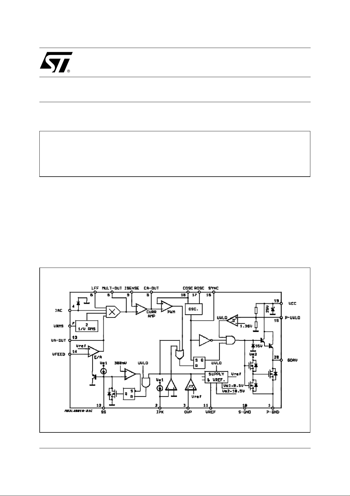
L4981 PFC Controller
This application features the L4981 P FC contr oller. It is a high per formanc e dev ice operating in average current
mode with many on-ch ip functions. The driv er output stage can deli ver 1.5A, which is very important for this type
of application.
A detailed device description can be found in AN628. A functional block diagram is shown in Figure 1.
Figure 1. Funct i on a l Di agram
November 2002
1/18
Page 2
AN1606 APPLICATION NOTE
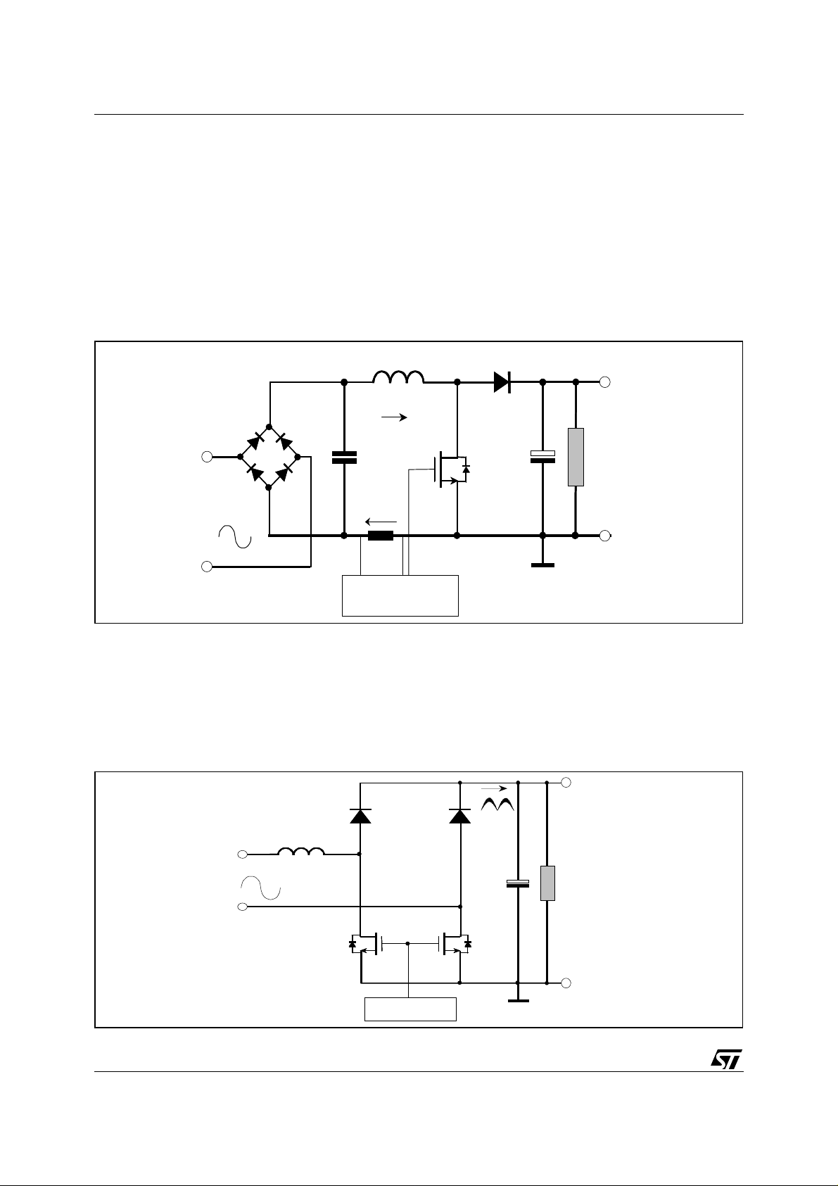
Description of "Bridgeless PFC Configuration" Topology
The conventional boost topology is the most efficient for PFC applications. It uses a dedicated diode bridge to
rectify the AC input voltage to DC, which is then followed by the boost section. See Figure 2.
This approach is good for a low to medium power range. As the power level increases, the diode bridge begins
to become an important part of the application and it is necessary for the designer to deal with the problem of
how to dissipate the heat in limited surface area. The dissipated power is important from an efficiency point of
view.
Figure 2.
Inductor
D
L
Load
A
M
Mains
V_Rs
Rs
controller
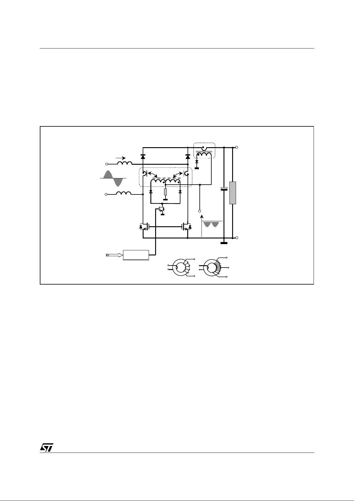
The bridgeless configuration topology presented in this paper avoids the need for the rectifier input bridge yet
maintains the classic boost topology.
This is easily done by m aking use of the intrinsic b ody diode c onnected between drain and s ource of P owerMOS
switches.
A simplified schematic of the bridgeless PFC configuration is shown in Figure 3.
Figure 3.
D1
Inductor
Mains
D2
L
O
Load
A
D
2/18
M1
M2
Controller
Page 3
AN1606 APPLICATION NOTE
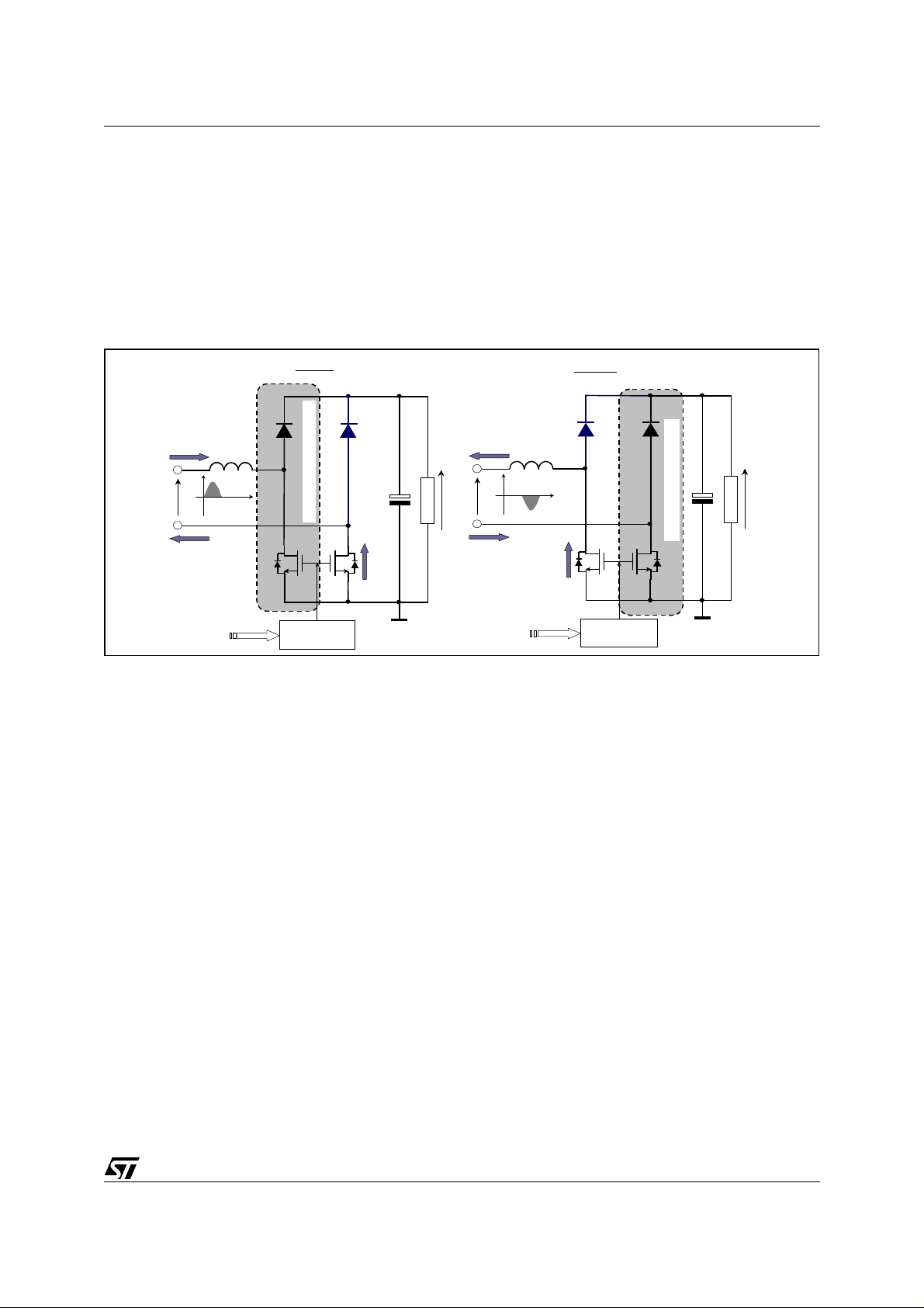
The circuit shown from a functional point of view is similar to the common boost converter. In the traditional topology current flows through two of the bridge diodes in series. In the bridgeless PFC configuration, current
flows through only one diode with the PowerMOS providing the return path.
To analyze the circuit operation, it is necessary to separate it into two sections. The first section operates as the
boost stage and the second section operates as the return path for the AC input signal.
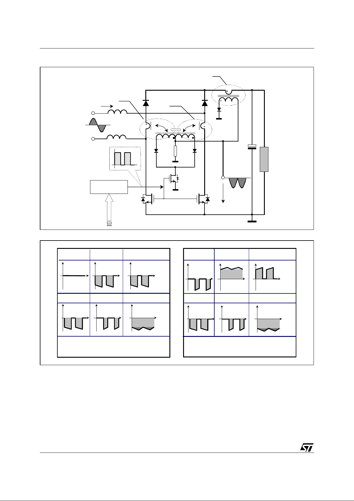
Referring to Figure 4, the left side (Figure 4a) shows curr ent flow dur ing the po sitive half cyc le and the right s ide
(Figure 4b) shows current flow during the negative half cycle
Figure 4.
Posit ive half cycle
Fig4a
L
v
in
D
1
M
1
controller
C
D
2
H
O
P
P
E
R
M
2
return
L
O
v
0
A
D
Fig4b
v
in
L
return
Negative half cycle
D
1
M
M
1
controller
D
2
C
H
O
P
P
E
R
2
L
O
v
0
A
D
Positive "HALF Cycle."
When the AC input voltage goes positive, the gate of M1 is driven high and c ur rent flows from the input through
the inductor, storing energy. When M1 turns off, energy in the inductor is released as current flows through D1,
through the load and returns through the body diode of M2 back to the input mains. See Figure 4A
During the-off time, the current throw the inductor L (that during this time discharges its energy), flows in to the
boost diode D1 and close the circuit through the load.
Negative "HALF Cycle".
During the negative half cycle circuit operation is mirrored as shown in Figure 4B. M2 turns on, current flows
through the inductor, storing energy. When M2 turns off, energy is released as current flows through D2, through
the load and back to the mains through the body diode of M1.
Note that the two PowerMOSFETs are dr iven synchronously. It doesn't matter whether the sections are performing as an active boost or as a path for the current to return. In either case there is benefit of lower power
dissipation when current flows through the PowerMOSFETs during the return phase.
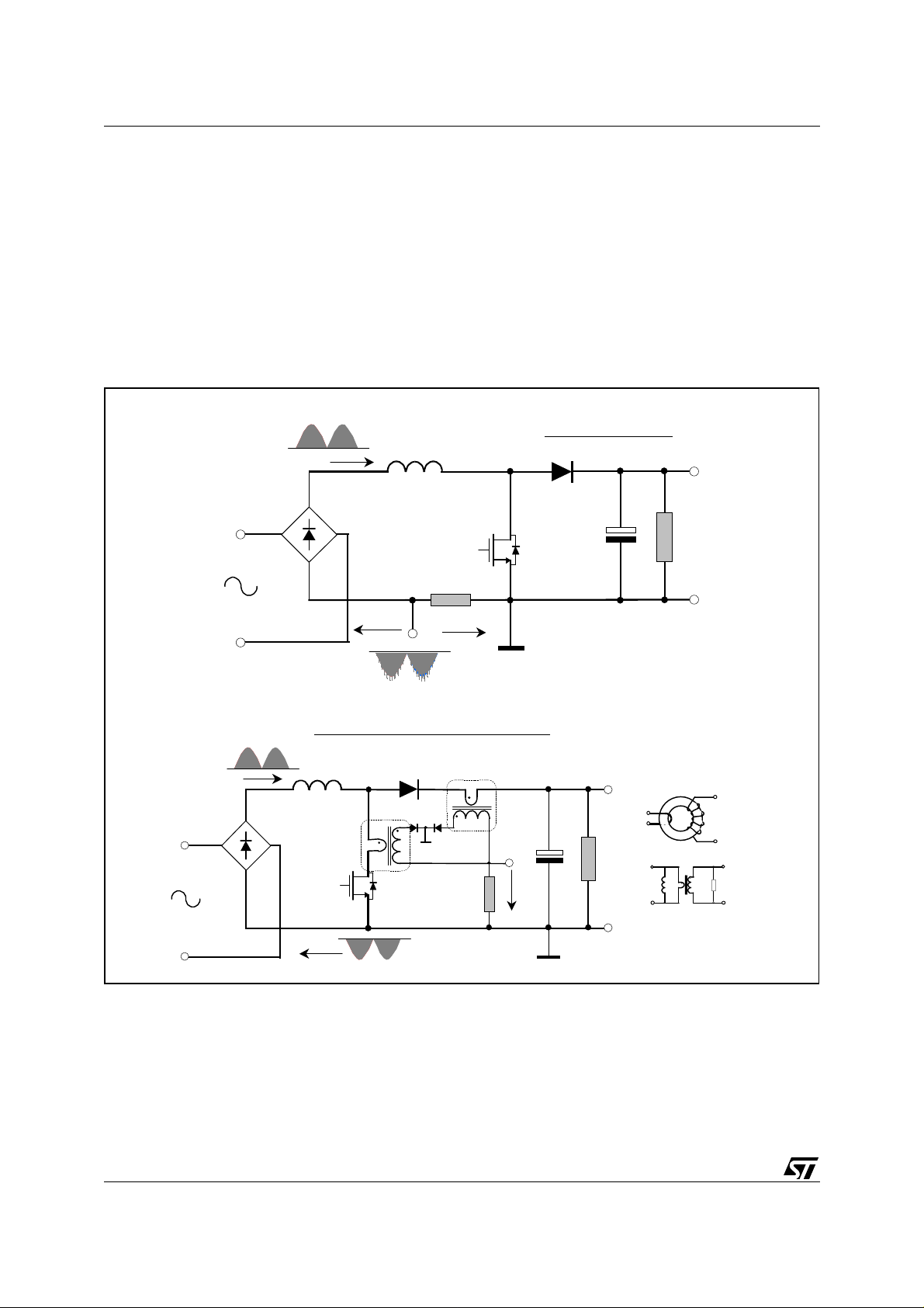
Current Sensing.
The PFC function requires controlling the current drawn from the mains and shaping it like the input voltage
waveform. To accomplish this it is necessary to sense the current and feed its signal to the control circuit.
In average current conventi onal boost topol ogy, we sense the rectified current rather than the AC input current.
This can be achieved by a simple sensing resisto r in the return of the current to the bridge, as shown in Figure5a.
3/18
Page 4
AN1606 APPLICATION NOTE
The L4981A/B current loop is designed to handle this negative signal. This type of resistor current sense can
easily be achieve in medium power applications. For high power PFC circuits it is necessary to use a magnetic
current transformer for improved efficiency as shown in Figure 5b.
In the bridgeless PFC configuration since an input rectifi er bridge is not used, the current is continuously changing its direction and the complexity of current sensing with a simple resistor can increase. Also in high power
applications, resistor sensing may dissipate too much power. In these cases, current sensing with a current
transformer is the preferred approach.
A current sense transformer core is typically high permeability ferrite (toroidal or a small core set). The primary
of the transformer is a single turn of wire through the core. The secondary typically consists of 50 to 100 turns.
Figure 5. .
IL
IL
Fig.5b
Fig.5a
Inductor
R
s
v
s
Iret.
Magnetic sensing for high power
Inductor
R
s
v
s
Standard Sensing
Typical sense transformers
Lm_p
1:n
Rs
Iret.
This type of sense transformer c annot oper ate at low frequency and for this reason it must be connected w here
the current is switched at high frequency. The magnetic core must be allowed reset.
This is normally accomplished by using a diode. In order to reproduce the inductor's current in boost topology,
two of magnetic sense sections are needed and the simplified schematic is shown in figure 5b.
When the sense transformer solution is applied in the bridgeless topology, the simple sense as in fig5b, is no
longer valid.
4/18
Page 5
AN1606 APPLICATION NOTE
The circuitry is more complex than in the boost case because here we have two pair of PowerMOS (M1, M2)
and diodes (D1, D2) alternating.
It is necessary to sense the chopping current of the (PowerMOS + diode) section and to sum the signals to be
applied to Rs.
The sensing of the diode's current can be simply done by placing a magnetic sensor at the common cathode
(L2 in fig.6.). Only one of the two diodes operates each half input cycle.
Figure 6.
L2
i
in
D
1
D
2
L1
L
R
s
O
A
D
Q1
v
M
1
controller
M2
Structure of sense transformers
L2 L1
s
For the PowerMOSFET portion of the circuit, the complexity increases because during the half cycle when one
of the PowerMOSFETs is chopping, the other one has to handle the current flowing back to the mains.
Using the configuration of sensors as shown in Figure 6 it is possible to solve the problem without undue complexity. The unnecessary high frequency portion of the cur rent signal is cancell ed because of the method M1 is
connected to L1A as shown in Figure 6b. The problem due to the change of polarity during each half cycle is
solved by using a center tapped secondary and two rectifiers.
Since the coupling of the two windings must not permit the demagnetization of L1, an auxiliary transistor Q1 is
used that opens the c ircuit during the off-time. For the L4981 c ontroller, the off- time is guaranteed no t to be less
than 5% of the period. Q1 can be a small signal transistor because its switched current is low due to the fact
that the transformer secondary will have a large number of turns.
To realize the current sensing transformer, a high permeability toroidal core (ur=>5000) has been used. The
secondary has 50 turns as a compromise to reduce secondary current yet not require a large number of turns.
5/18
Page 6
AN1606 APPLICATION NOTE
Fig 6b
L2
L1a
Φ
i
in
Inductor
controller
L1b
Φ
L1a
D
M
1
L1=L1a+L1b
Φ
L1b
1
D
2
Dc
Φ
Da
R
s
Db
Q1
v
M
L1a
s
2
L1b
ΦΦ
L
O
A
D
L1=L1a+L1b
Φ
L2L1 TOT
v
s
v
s
v
R
s
M2_D2 Chopping Phase
Other control circuits
Input voltage sensing: in the standard boost topology the rectified in put voltage wavefor m is sensed using a resistor that, by one internal circuit, delivers the mirrored signal to one of the multiplier's inputs (Iac-pin4).
For the bridgeless configuration see the circuit shown in fig.7.
6/18
L1
v
sa
L2
v
sb
TOT
v
R
s
M1_D1 Chopping Phase
Page 7

Figure 7.
AN1606 APPLICATION NOTE
A
Coupled
Inductor
R
1
v
(t)
L
C
iac(t)
1
R
CURRENT
MIRROR
R
1
2
vL(t)
B
R
1
(t)
i
+
R
C
1
1
ac
R
2
Input voltage sensing (A), and equivalent circuit (B).
It is based on the following consideration: the fr equency of the signal of interest (tens of H z), is much lower than
the switching frequency (tens of kHz). The boost inductor, for the low frequency, behaves like a short circuit.
Since the Powermos's drains are, in turns, close to ground (via the body diode), the resulting equivalent circuit
is shown in fig7b.
The relation between the voltage (from the inductor) and the current that flows in to Iac pin is:
1
1
--------------
-----------
a)
Ys()
Req
⋅=
1st+
R1
fp
------- -
//R2 C1⋅=
2
1
---------------- -=
2 π t⋅⋅
Where: and
Req R1 2 R2⋅+= t
The net introduces one pole at:
The pole must be located at a frequency high enough not to distort the input waveform and at the same time,
low enough to filter the switching frequency.
In this application the equivalent resistance has been choosen
Ω
Req.=324-k
The resulting R1 is 300k
that fits well with the current amplifier design.
Ω
and R2 is 12k
Ω
The pole has been placed a decade before the switching frequency:
Fp = 5kHz that gives:
b)
C1
-------------------------------------------------- 2.87nF==
2 π fp
1
⋅⋅ ⋅
R1
------- -
//R2
2
In practice, in our test, a standard value of 2.7 nF as ben used.
7/18
Page 8

AN1606 APPLICATION NOTE
K
LP
R
c
Ra 2Rb 2Rc
++
()
------------------------------------------------ -=
Voltage feed-forward.
Voltage feed-forward, a useful function in wide range applications, requir es a DC voltage proportional to the rms.
value of the input mains. For the L4981, this value must be between 1.5V to 5.5V so that it can mirror over a
wide range.
Since the rectified mains frequency is 100 -120Hz, we need a large rejection for this frequency and because the
feed-forward reaction time is proportional to the bandwidth, we introduce a second order filter that allows good
compromise between attenuation of the fundamental frequency and response time.
The circuit (Fig.8) is similar to the fig.7 described earlier.
Figure 8.
Coupled
Inductor
A
R
a
R
C
a
b
C
b
R
a
R
c
vLP(t)
Voltage fe ed -forward Circuit (A) an d eq u i valent circui t (B).
B
R
a
+
R
C
a
R
b
vLP(t)
a
C
b
R
c
Defining HLP(s) the transfer functions between the vol tage fr om the inductor and the v oltage at the output o f the
filter v
c)
(Fig.8B), we have the following relation:
LP
H
LPKLP
-------------------------------------------------
=
1st
1
+()1st
1
+()⋅
2
The time constants c annot be ex pressed i n sim ple w ay and so that th e positi on of poles can be numeric ally calculated.
The constant K
is defined taking in to account the wide-range that is, V_mains is between 88V and 264V:
LP
d)
Choosing to calculate this value at the midpoint of the allowed values:
e)
8/18
V
LPVRMS
88 264+
22
---------------------- -
---------- -
π
2
22
---------- -
π
K
⋅=
LP
K
LP
1.5 5.5+
---------------------- -=⋅⋅
2
Page 9

AN1606 APPLICATION NOTE
To fit this, it has been choosen
Ra 998kΩ 2499⋅()≡=
For the capacitors, we set 80 dB of attenuation on the fundamental frequency using the commercial values: -
The design places two poles at 3Hz and 14Hz and 80 dB of attenuation at 100Hz.
Practical examples.
The preceeding points of this note have described the topology peculiarity. Remainder of the topics, for PFC
design, are similar to standard P.F.C. boost applications based on L4981A/B (see the related references and
application notes).
Starting from now, we can refer to real design examples.
In fact, in order to verify the efficacy of the described configuration, it have been checked a pair of application's
size. For evaluation porpoise, it has been realized a printed circuit.
Rb 150kΩ=
Rc 30kΩ=
Ca 390nF=
Cb 470nF=
Let us beginnes with and 800W P.F.C application.
800W Target:
1 - Wide range input voltage variation 110Vrms to 220Vrms.
2 - Output power 800W.
2 - Output voltage 400Vdc.
A switching frequency of 50 kHz has been chosen as a good compromise between the coil-size and the pow-
erMOS switching losses.
Boost Inductor design.
To design the boost inductor, the parameters under consideration are the percentage current ripple (as low as
possible) and the cost of the bobbin. This portion of the design is the same as for the standard topology.
In this application, in place of a single inductor connected to one of the phases, it has been chosen to split the
inductor into two sections (two windings on the same core) as shown in the connection diagram at fig.9.
9/18
Page 10

AN1606 APPLICATION NOTE
Figure 9. Con nection Diagra m for t he C ou pl ed I nductor
i
L
Inductor
Mains
Mains
Z
in
Leq.
Z
in
Equivalent circuit.
vs(t)
is(t)
vs(t)
is(t)
Realizing the inductor in this manner improves common mode rejection and avoids the effect of the difference
between drain capacitance of the PowerMOSFETs. In or der to simplify the model , assume a near un ity coupling
factor and the equivalent circuit is shown in Figure 9b.
The inductance is proportional to the square of the number of turns. For the two windings it will be:
N
N′
f)
and
----=
2
N
N ′ total
N
--- -
--- -+=
2
2
The required number of turns for a given inductance on the same core is the same as it is for one winding or
two windings. The only difference is that the two windings are separated into two sections. For simplicity we can
design the coupled inductor using the same criteria as for a standard inductor - core size, number of turns, and
size of copper wire.
For the core, the preferred design is a gapped ferrite core set.
The size of the core can be chosen c onsidering the maximum current Ipk . that, for the 800W target's parameters
can exceed 14A (placing Ipk. = 15A).
g)
Where:
V
≥ KLI
coreVcore ""min
K1.410
,
lcore
4
--------------
⋅⋅=
lgap
2
peck (mm
3
)⋅⋅=
For the 800W application, the nominal current ripple has been chosen around 25%. This fixes the boost induc-
µ
tance value L=450
10/18
H.
Page 11

AN1606 APPLICATION NOTE
The coil requirements can b e met usi ng a gapped c ore set type E66/33/27, character iz ed with the follow ing k ey
parameters:
Ae = 550mm^3; lcore = 146mm; m_core = >1600;
Vcore = 80.4*10^3mm^3
The air gap needed to avoid saturation and optimize the coil size is equal to lap = 3mm.
Using the parameters in the formula g).
Vcore>67.5mm^3
This result confirms the core is well above the minimum size.
The used formula for the number of turnes, needed to design the total required inductance L, is:
h)
l core,
L
------
µ
0
-----------------------------
core A⋅,
µ
r
N
1gap
---------------------------------------------+⋅=
π
-- -
A
4
2
1gap⋅+
The resulting N=38, in our solution, has been realized with 19 turns +19 turns.
In order to minimize the high frequency losses, the winding has been made using the "multiple wire" approach.
It is possible to estimate the losses for a low frequency current.
Imposing a maximum power value to be dissipated in the copper (Pcu = 5W)
i)
P
wire
RDCI
2
,
RMS m ax
5W <⋅= R
DC
P
wire
------------------------ - 60mΩ=<
2
I
,
RMS m ax
Using the formula for multiple wires: -
l)
R
DCρCu
-----------------------
π
-- -
d
4
60mΩ<⋅=
2
M⋅⋅
l
N⋅
turn
Were:
In practice 20 wires were used, each having a diameter d=0.4 mm.
Output Capacitor filter.
For the bulk capacitor selection, we consider a reasonable 100Hz voltage ripple.
11/18
Page 12

AN1606 APPLICATION NOTE
m)
Co
---------------------------------------------------=
2 π 2f∆fo Vo⋅⋅⋅⋅⋅
Po
were f is the input frequency.
Imposing <10Vac the peak of voltage variation over 400Vo, the Co value will results >318
value is 330
µ
F
µ
F; the commercial
Power Devices.
The selection of the power devices is dependent upon the topology and the size of the application.
Operating in continuous current mode, fast reverse recovery diodes are needed.
The TURBOSWITCH "STM family", in the 600V voltage range, offers a very good solution for the two boost
diodes, the STTH8R06FP has been chosen.
The insulated TO-220 package makes it easy to assemble the parts on a heat sinke.
Concerning the Powermos requirements, a 500V blocking voltage (Bvdss) is needed, for this application.
The chip selection is more complex. To find the best solution, it must be considered all the parameters that affect
the power dissipation and to compare the results in terms of a cost to benefit ratio. The devices used in the 800W
application (2+2), are the type STY34NB50F.
The four Powermos are effic iently dr iven without any add itional buffer, thanks to th e smart c har acteristi cs of the
integrated driver.
Figure 10. 800W SCHEMATHIC DIAGRAM.
R
C
Input
R
27
R
24
15
F
1
C
1
R
28
R25R
Vcc
C
16
C
13
DETAIL for L2
L
2a
L
2b
D1+D2+D3+D
L
1
R
29
26
R
23
R
L
2c
R
32
R30R
C
22
1
4
Dz
R
33
31
14
Vcc
C
1
2
D
5
L
2a
Q1Q
2
R
D
2
D
7
8
R
3
4
7
10
19
15 16
1
Vcc
D
6
L
2b
D
11
Q
3
Q
4
Q
R
D
9
R
4
R
6
5
D
5
10
R
7
20 8
L4981A/B
C
R
12
21
C
11
L
3
D
13
L
2c
D
R
95
R
12
8
R
R
9
10
C
2
R
17
11
6
18
R
17
12
C
3
13
14
R
19
C
10
20
NTC
R
R
11
14
C
C
3
4
R
R
12
15
R
R
13
16
5
C
6
C
7
18
8
12/18
Page 13

AN1606 APPLICATION NOTE
B.O.M. for 800W Bridgeless Evaluation Circuit.
Name Value Name Value Name Value Name Value Name Value
R
1
R
9
R
17
R
22,24,27
C
1,3
C
7
C
13
NTC
L
2,#(1/ 50+50)
68
Ω R
2.7 kΩ R
3.9kΩ R
30 kΩ R
1 µF
1.8 nF C
470 nF C
2.5
2,3,4,5
10
18
23,30,31,32,33
C
2
8
14
B57364
# sense transformer; L
10
Ω R
1.5 kΩ R
27
k
150 kΩ R
11,12,14,15
Ω R
25,26,28,29
220 µF
1 µF
2.7 nF C
3#(1/50)
1.8
6
Ω R
1 MΩ R
19
220 kΩ R
499 kΩ R
C
4
C
10
15
330 µF
120 nF C
100 nF C
F1
# sense transformer
C
20A
7
13
20
34
5
11
16
#Ferrites Hy_perm.' Diam.=20mm
D
; D
1,2,3,4
=450 µH; => E66*33*27-18+18 turns 3mm/gapped# 20 wires //m=0.4 mm each.
L
1
7,8,9,10,11,12,13
= 1N4148 ; Dz1 = 1N4746; Q5 = BS170
100
Ω R
22
kΩ R
2.7 kΩ R
8
16
21
5 Ω
25.5 kΩ
5.6 kΩ
12 kΩ RSN 12 Ω
10 nF C
1 nF C
6
12
1 µF
5.6 nF
390 nF
= STTH8R06FP; Q
D
5,6
Note:
For the evaluation circuit and external coupled inductor EMC where utilized.
=STY34NB50F
1,2,3,4
The filter has been achieved as follows: Coupled inductor (30 + 30) turns; wire diameter = 0.8mm on a toroidal (40x17x9 mm): Magnetizing inductance (each half inductor) Lm=8mH and a leakage inductance, Ld=50
µ
H.
Scaling down the application.
As a second step, based on the same circuit, a 600W P.F.C. has been built.
The target specification designed for server application is.
600W Target:
1- Wide range input mains 110Vrms to 220Vrms.
2- Output power = 600W.
2- Output voltage = 400Vdc.
The switching frequency has been set at 75kHz to use a reduced size and high performance PowerMOS.
13/18
Page 14

AN1606 APPLICATION NOTE
Boost Inductor design.
The boost inductor has been design as been previously described .
For the 600W application, the nominal current ripple has been set around 22%, gives requires the inductance
value L=440
The inductor requirements can be met using the core set type E55/28/21, characterized with the following key
parameters:
A = 357mm^2; lcore = 123mm; m_core =>1600;
Vcore = 43.7mm^3
µ
H.
The needed air gap is: l
=2.5mm.
ap
Using the relation g), Vcore>38.8mm^3
The result confirms that the core is good enough.
h)
Using the relation
, the resulting N=42.
For the 600W, the coil has been realized with 21 turns +21 turns.
For minimize the high frequency losses, the "multiple wire" solution has been used.
Imposing the copper losses (Pcu = 3.8W), it has been used 14 wires having a diameter d = 0.4 mm each.
Output Capacitor.
For the selection of CO, the relation as been described in (m). The commercial value = 330µF/450V used for
the 800W application is still good for the 600W application.
Power Devices.
For the two boost diodes, as for the 800W application, the STTH8R06FP has been used.
Concerning the Powermos, the devices used in the 600W version application are two STW26NM50F.
14/18
Page 15

Figure 11. 600W SCHEMATHIC DIAGRAM.
R
Input
R
R
C
27
24
15
F
1
C
1
R
28
R25R
Vcc
C
16
C
13
DETAIL for L2
L
2a
L
2b
D1+D2+D3+D
L
1
R
29
26
R
23
R
L
2c
R
32
R30R
C
22
1
4
Dz
1
R
33
R35
31
14
R36
Vcc
C
2
D
5
L
2a
Q
2
R
D
3
8
16
4
7
10
19
1
15
Vcc
D
6
L
2b
D
11
Q
3
D
9
R
4
R
6
Q
20 8
L4981A/B
C
R
12
21
C
11
AN1606 APPLICATION NOTE
L
3
D
L
R
8
5
R
7
95
R
20
13
2c
D
12
R
R
9
10
C
5
2
R
17
11
6
18
17
12
3
13
14
C
C
C
R
18
C
8
R
19
C
10
NTC
R
R
11
14
C
C
3
4
R
R
12
15
R
R
13
16
6
7
9
B.O.M. for 600W version Bridgeless Evaluation Circuit.
Name Value Name Value Name Value Name Value Name Value
R
1
R
9
R
17
R
22,24,27
C
1,3
C
7
C
13
NTC
L
2,#(1/ 50+50)
68
Ω R
2.7 k
Ω R
3.9k
Ω R
30 k
Ω R
1 µF
1.8 nF C
470 nF C
2.5
3,4
10
18
23,30,31,32,33
C
2
8
14
B 57364 F1 15 A
# sense transformer ; L
10
Ω R
1.5 k
Ω R
11,12,14,15
33 k
Ω R
150 k
Ω R
25,26,28,29
220 µF
1 µF
2.7 nF C
6.8
6
19
C
4
C
10
15
Ω R
1 M
Ω R
220 k
Ω R
499 k
Ω R
330 µF
120 nF C
100 nF C
3#(1/50)
7
13
20
34
C
5
11
16
# sense transformer
100
Ω R
22 k
Ω R
2.7 k
Ω R
12 k
Ω
10 nF C
1 nF C
390 nF
8
16
21
6
12
#Ferrites Hy_perm.' Diam.=20mm
D
1,2,3,4 D8,9,11,12,13
=1N4148; Dz1=1N4746; Q5 = BS170.
6.8
25.5 k
5.6 k
1 µF
5.6 nF
15/18
Ω
Ω
Ω
Page 16

AN1606 APPLICATION NOTE
L1=440 µH; => E55*28*21-21+21 turns 2.5mm/gapped# 14 wires // m=0.4 mm each.
D
= STTH8R06FP; Q
5,6
Note:
For the evaluation circuit and external coupled inductor EMC where utilized.
The filter has been achieved as follows: Coupled inductor (30 + 30) turns; wire diameter = 0.8mm on a toroidal (40x16x8.5 mm): Magnetizing inductance (each half inductor) Lm=8mH and a leakage inductance, Ld=50uH.
Conclusion:
The innovative bridgel ess PFC confi gur ation as descri bed in this applic ation note has been suc cessful ly tested.
Details have been presented how to implement the technology, which should prove interesting to designers.
Figure 12 shows the test results of efficiency and power dissipation for the application's 800W prototype.
Figure 12.
[%]
[%]
[%]
98
98
98
B.Less
B.Less
97
97
97
96
96
96
B.Less
Standard PFC
Standard PFC
Standard PFC
= STW26NM50F
2,3
EFFICIENCY
EFFICIENCY
EFFICIENCY
95
95
95
94
94
94
P0=800 W
P0=800 W
93
93
93
92
92
92
88 110 132 154 176 198 220 242 264
88 110 132 154 176 198 220 242 264
88 110 132 154 176 198 220 242 264
DISSIPATED POWER
DISSIPATED POWER
DISSIPATED POWER
DISSIPATED POWER
[w]
[w]
[w]
[w]
80
80
80
80
70
70
70
70
60
60
60
60
50
50
50
50
40
40
40
40
30
30
30
30
20
20
20
20
10
10
10
10
P0=800 W
P0=800 W
P0=800 WP0=800 W
0
0
0
0
88 110 132 154 176 198 220 242 264
88 110 132 154 176 198 220 242 264
88 110 132 154 176 198 220 242 264
88 110 132 154 176 198 220 242 264
B.Less
B.Less
B.Less
B.Less
B.Less
Standard PFC
Standard PFC
Standard PFC
Standard PFC
Standard PFC
P0=800 WP0=800 W
V
V
V
in
in
in
V
V
V
V
in
in
in
in
16/18
Page 17

AN1606 APPLICATION NOTE
Evaluation results for the 800W version.
@Vin=110Vac: Nominal power
Vout Pout Pin PF TDH Efficiency
395VDC 800W 860W 0.999 4 94%
@Vin=220Vac: Nominal power
395VDC 800W 824W 0.997 8 97%
Evaluation results for the 600W version.
@Vin=110Vac: Nominal power
Vout Pout Pin PF TDH Efficiency
395VDC 652W 700W 0.998 6.7 93%
@Vin=220Vac: Nominal power
395VDC 652W 624W 0.994 9 96.5%
References: a)
Parsad N. Enjeti, R. Martinez "A high performance single phase AC to DC rectifier with input power factor
correction" IEEE APEC'93
b)
Alexandre Ferrari de Souza and Ivo Barbi "A new ZVS Semi resonant High Power Factor Rectifier with Re-
duced Conduction Losses"
IEE TRANSACTIONS ON INDUS TRIAL ELECTRONICS, VOL.46, NO.1 FEBRUARY 1999.
c)
STM Application Notes AN628; AN824.
STMicroelectronics @ www.st.com, http://ccd.sgp.st.com/stonline/books/index.htm
17/18
Page 18

AN1606 APPLICATION NOTE
Information furnished is believed to be accurate and reliable. However, STMicroelectronics assumes no responsibility for the consequences
of use of such information nor for any infringement of patents or other rights of third parties which may result from its use. No license is granted
by implic ation or otherwise under any patent or patent r i ght s of STMi croelectr oni cs. Specifications menti oned in thi s publication are s ubj ect
to change without notice. This publication supersedes and replaces all information previously supplied. STMicroelectronics products are not
authorized for use as cri tical components in li f e support dev i ces or systems without express writ t en approval of STMicroel ectronics.
The ST logo is a registered trademark of STMicroelectronics
2002 STMi croelectronics - All Ri ghts Rese rved
Australia - Brazi l - Canada - Ch i na - F i nl and - France - Germany - Hong Kong - India - Israel - Italy - Japan -Malaysia - Malta - Morocco -
Singap ore - Spain - Sw eden - Switzerland - U ni t ed Kingdom - United St at es.
STMicroelectronics GROUP OF COMPANIES
http://www.s t. com
18/18
 Loading...